Note: Descriptions are shown in the official language in which they were submitted.
. -- :
.` '~1 3~68 6
D-93-1-453 -1- PATENT APPLICATION
~,
INCANDESCENl~ LAMP HAVING HARDGL.ASS ENVELOPl~
WIl'H IN~ERFERENCE FILI'ER
CROSS-REFEREN(:E TO RELATED
APPLICATIONS
' U.S. patent application Serial No. (Attorney
Docket No. D-93-1-452) ~iled concurrently herewith and
assigned to the same assignee of the present
invention, relates to the present invention.
FIELD OF THE INVENTION
This invention relates in general to electric
incandescent lamps and pertains, more particularly, to
incandescent lamps operating by a tungsten-halogen
cycle.
BACXGROUND OF THE INVENTION :
Thin film optical coating~ known as interference -~
filters which comprise alternating layer-~ of two or
~: 25 more materials of different indices of refraction are ~;
well known to those skilled in the art. Such coatinqs
or films,are used to selectively reflect or transmit
light radiation from various portions of the :~;
I electromagnetlc radiation spectrum such as
~;l
~13~686
. , ,
.
, D-93-1-453 -2- PATENT APP~ICATION
, .,
.,
!,i
.~
: ultraviolet, vi,ible and infrared radiation. These
films or coating~ are u~ed in the lamp industry to
, coat reflectors and lamp envelopes. One application
in which these thin film optical coatings are useful
, 5 is to improve the illumination efficiency or efficacy
~ of incandescent lamps by reflecting infrared energy
,l emitted by a filament bac}; to the filament while
transmitting the visible light portion of the
, electromagnetic spectrum emitted by the filament.
' 10 Thls lower~ the amount of electrical energy required
to be supplied to the filament to maintain its
operating temperature. In other lamp applications
3 where it is desired to transmit infrared radiation,
~, such filteri can reflect the shorter wavelength
portions of the spectrum, such as ultraviolet and
visible light portions emitted by the filament and
transmit primarily the inrared portion in order to
provide heat radiation with little or no visible light
radiation. Such an application of this latter type
would include a typical radiant heater for residential
or indu~trial use where visible radiation emitted by
the heater is unneeded or undesirable.
Interference filters for application where the
filter will be exposed to high temperature (in excess
of 500- C. or so) have been made of alternating layers
of tantala (tantalum pentoxide Ta2Os) and silica
SiO2~, wherein the ,ilica is the low refractive index
material and the tantala i3 the high refractive index
material. Such filters and lamps employing same are
~, .;: , . ! ~ '
~13~686
., I
D-93-1-453 -3- PATENT APPLICATIOIN
disclosed, for example, in U.S. Patent Nos. 4,588,923;
4,663,557 and 4,689,519. In such lamp applications
the interference filters, which are applied on the
outside surface of the vitreou~ lamp envelope
containing the filament within, often reach operating
temperatures in the range o~E from about 800- to 900
C.
When such interference filters are applied to a
tungsten halogen lamp, the operating temperature of
the envelope wall of the lamp increases. This
increaqe in the lamp wall temperature can be in excesR
of 100- C. for certain lamp shapes and wattages. The
wall temperature can be lowered by increasing the
distance from the filament to the envelope wall,
however, due to the effects of imperfect geometries of
the envelope wall and the coil, it i8 desirable to
have the envelope wall as close to the filament as is
practical. Due to the combination of hiqh wall ~;
temperatures and small capsule sizes, high efficiency
infrared conserving tungsten halogen lamps have
heretofore been limited to the use of quartz for their
envelope material. ~
When selective interference filters such as ;
alternating layers of tantalum pentoxide and silica
are deposited on quartz using a process that is
suitable for formlng unlform coatings on complex
shapes,jthe resulting film is sub~ected to stress that
can cause the film to crack and peel. Methods for
reducing the stress in the films are described, for
.~3
~, ~
135686
. ,
D-93-1~453 -4- PATENT APPLICATION
j example, ln U.S. Patent Nos. 4,701,663 and 4,949,005.
'f For example U.S. Patent No. 4,949,005 teaches a method
of heat treating the films to produce a randomized
crack pattern ln the film which results in a film with
strong adherence to the substrate and good optical
properties. However, any cracks in the optical film
will cause the light which strikes the crack to
scatter, thus compromising the integrity of the
optical system of which the lamp is a part and
reducing the magnitude of the efficiency gain.
In operation, tungsten-halogen lamps normally
contain a non-reactive qas filling such as neon,
nitrogen, argon, krypton or xenon or combination
thereof together with iodlne, bromine, chlorine or
fluorine vapor which combines with the evaporated
tungsten escaping from the incandescent filament. An
equilibrium concentration is attained by the qaseous
species within the lamp between the temperature limits
defined by the incandescent filament and coldest spot
in the lamp envelope. The cold spot temperature must
be sufficiently high to prevent any tungsten halide
from condensing, and providing that this condition ls
met a continuous tunqsten transport cycle operate~
which keeps the envelope free from tungsten. The
minimum envelope temperature depends upon the halogen
or halogens taking part in the cycle.
Hardglasses, such as borosilicate or
aluminosilicate glass, have been successfully used for
the envelope in certain generally low-wattage,
~11 3~686
., ,
. `~ !
O--93-1-453 -5- PATENI' APPLICATION
,"
. .
tungsten-halogen lamps. However, as the lamp wattage
is increased or the size of the lamp envelope is
decreased, the increased wall temperature causes an
increase in the rate of diffusion of the alkaline ions
of the hardglass (i.e., barium, strontium and calcium
ions) to the inner surface of the glass where they are
able to react with ~he halogen gas. The result is a
permanent condensation of the thus reacted halogen gas
on the inner walls of the lamp, which reduces the
available halogen in the lamp to a level where the -
tungsten/halogen cycle no longer operates, causing the
lamp to blacken. After the onset of blackening, the
~ wall temperature of the blackened portion of the bulb
'j wall will increase, causing a more rapid diffusion,
and further blackening in a "runaway" type reaction.
These high temperature reactions have often limited
the use of hardglass in tungsten-halogen lamps where
, the glass will be sub~ected to high temperatures.
;I "FT-IR Diagnostics of Tungsten-Halogen Lamps: Role of ;
Halogen Concentration, Phosphorus, Wall Material, and
i Burninq Environment", (1991~, by Laurence Bigio et al,
shows that for a tungsten-halogen capsule burning in a
Parabolic Aluminized Reflector (PAR) lamp with a "hot
spot" temperature of 600- C., the level of hydrogen
bromide available in the gas phase decreases with
burning time in a hardglass tungsten-halogen lamp,
whereas the level of hydrogen bromide available in' the '~'A'
gas phase remained at or above its initial levels in a
quartz tungsten-halogen lamp.
:
.
~`~:
6 8 6
D-93-1-453 -6- PATl:N~ APPLICl~TION
'. .
It ls undesirable to manufacture the lamps with
excess halogen to compensate for the halogen which may
react during the life of the lamp. This is because
the excess halogen will react with the cooler portions
of the filament and the lead wires over time, which
will cause short life in larnps with long rated life,
for example, greater than 750 hours.
The problem of excess activity is even more
pronounced in lamps with fine wire filaments, for
example, 50 wat~, 120 volt filaments, since these
thinner filaments have smaller cross sections and will
not withstand halogen attack for very long before they -
fail.
In view of the limitations of using hardglass
for the envelope of a tungsten-halogen ~ncandescent
lamp, the envelope of such lamps is often made from
vitreous fused silica ~i.e., quartz) or a high silica
content glass such as one composed of ninety-six per
cent silica and sold under the trademark Vycor.
However, quartz and ninety-six per cent silica glass
are difficult to process and require special seallng
techniqua~ to introduce the lead wires into the lamps
because of their low coefficients of expansion, and
thus leave something to be desired from an economic
standpoint.
To prevent the reaction of the halogen
constituents of the filling gas with various
constituent~ of the lamp envelope, it is well known to
use special glasses and/or a protective barrier layer.
1 ~1356~6
.' !
j:, D-93-1-453 -7- PATENT APPLICATION ~ ~
I
U.S. Patent No. 4,50~,991, which isisued to
Wurster et al on April 2, 1985, teaches a halogen-
cycle incandescent lamp with an envelope of a special
j soft glass wherein the inner surface of the bulb is
depleted of alkali lons (i.e., sodium and potassium ~
ions) to avoid a reaction between the halogen ;
constituents of the filling gas and the alkali
constituents of the lamp envelope. The vacancies thus
generated in the glass lattice may be filled by
` 10 replacement ions such as lithium, magnesium and
calcium. In another emibodiment, the soft glass ~`
envelope having its inner surface depleted of sodium
and potassium ion~ is coated with a protective layer
of a metal and/or semi-metal oxide such as silicon
lS dioxide (SiO2), titanium dioxide (TiO2) or barium
¦ oxide (B2O3). According to Wurster et al, reaction
between the halogen constituent of the filling gas and
alkali ions i5 avoided in prior known halogen cycle
incandescent lamps because the lamp bulb was
manufactured from quartz or hard glass which both
contaln either no or only minor proportions of alkali
ion~
U.S. Patent No. 3,496,401, which issued to
Dumbaugh on February 17, 1970, teaches an iodine-cycle
incandescent lamp having a lamp envelope consistinq
e~sentially of an aluminosilicate qlass composition `~
containing a low level o~ alkali metal oxide (e.gJ, `~
sodium oxide). According to ~he patent, no white
coatings will be formed in such a hardglass envelope
~13~686
.,
-` D- 9 3 -1- 4 5 3 - 8 - PATE~ APPLICATION
~.i,
.,
containing a maxlmum amount of 0.10% by welght of
~i alkali and having a strain ]point of at least the
.l envelope wall temperature. Upon incandescence of the
lamp filament, the envelope of the iodine-containing
q 5 lamp reaches an operating t~mperature of between 500-
,~ 700 C.
U.S. Patent No. 4,256,988, which issued to
Coaten et al on March 17, 1981, teaches a fluorine-
,j cycle incandescent lamp wherein the internal surface
of the lamp envelope and optionally also the exposed
surface of internal components of the lamp is coated
with a continuous imperforate coating composed of a
metal oxide such as aluminum oxide. The aluminum
oxide coating prevents free fluorlne from reacting
with solid tungsten and the fluorides from reacting
with the silica contained in the lamp envelope.
U.S. Patent Nos. 3,900,754; 3,902,091 and
3,982,046 teach the use of glassy coatings of metal
pho~phate~ or arsenates as protective coatings for the
internal surfaces of halogen-containing electric
lamps, and describe a process for the formation of
defect free coatings by deposition of a solution of
compounds of the metal and phosphorus or arsenlc,
followed by evaporation of the solvent and baking o~
the resulting layer.
Although the above-described techniques may be
effective to some degree, there i3 a need in the
industry for alternative ~olutions.
...... ~.~.. ... .; . .. .... .. .. ...... ... . . . .. .. . . . . . . ... . ..
~ ~13.S686
D--93-1-453 --9-- Pl~TENT APPLICATION
~,
SUMMARY OF ~{E INVENTION
It is, therefore, an ob~ect of the present
invention to obviate the disadvantages of the prior
art.
It ii~ still another ob~ect of the invention to
provide an improved incandescent lamp.
It is another ob~ect of the invention to provida
an incandescent lamp which can be more easily `
manufactured and does not re~uire special sealing
techniques to introduce the lead wires into the lamps. ~
It is still another ob~ect of the invention to ~`
provide an incandescent lamp having a hardglass
envelope which can effectively operate at higher wall
temperatures than normal for a tungsten/halogen lamp
and will be suitable for use in higher wattage and/or `~
more compact lamp designs. ~;~
These ob~ects are accomplished in one aspect of `i
the invention by the provision of an incandescent lamp
including a hermetically sealed envelope of hardglass
composed of a predetermined quantity of alkaline ions.
A fill material including an inert fill gas and a
halogen additive i~ contained within the envelope. A
coating of silicon dioxide iq disposed on a portion of
the internal surface of the envelope for preventing
the halogen additive from combining with the alkaline
ions of the envelope. At least one tungsten filament
is sealed in the envelope and supported by a pair of ;--
lead-ln wlre~. A coatlng for selective1y reflectlng
.
~.,'
~ ~ (,
~'"".'''''.'''`''';".''',,. ' ':`''
~'''.'''',''''".''.,'.'~, i",'." ',"
~135686
`;
^ D-93-1-453 -10- PATEN'r APPLICATION
, !
and tranismitting iselected portionis of the light
spectrum emltted by the filament is disposed on an
? external surface of the envelope.
;' In accordance with further teachings of the
present invention, the coating of silicon dioxide is
disposed on substantially the entire internal surEace
of the envelope. Preferably, the thickness of the
silicon dioxide coating is within the range of from
about 100 to 3000 Angstroms.
~ 10 In accordance with further aspects of the
i~ present invention, the lamp may include an outer
~ envelope of a molded light-transmissive glass body or;~ a reflector (e.g., elliptical or paxabolic). A base
may be disposed at one end of the lamp.
Additional ob~ects, advantages and novel
featureis of the invention will be set forth in the
description which follows, and in part will become
apparent to those skilled in the art upon examination
of the following or may be learned by practice of the
invention. The aforementioned objects and advantages
of the invention may be realized and attained by means
of the instrumentallt1es and combination particularly
pointed out in the appended claims.
BRIEF DESCRIPTION OF THE DRAWINGS
The invention will become more readily apparent
from the following exemplary description in connection
with the accompanying drawings, wherein:
~:l3~6g6
D-93-1-453 -11- PATENI APPLICATION
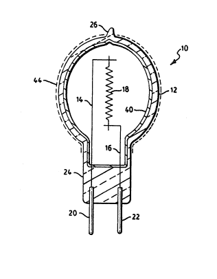
FIGS. 1 illu~trates a sectional view of an
incandescent lamp in accordance wlth a preferred
embodiment of the present invention;
`
FIG. 2 shows a sectional view of an incandescent
lamp having an elliptical reflector in accordance with
another embodiment of the present invention;
:
FIG. 3 shows a sectional view of an incandescent
lamp having an outer envelope in accordance with ~-
another ambodiment of the present invention; and
FIG. 4 shows a sectional view of a PAR
incandescent lamp having a parabolic reflector in
accordance with another embodiment of the present
invention.
BEST MODE FOR CARRYING OUT THE INVENTION
For a better under~tanding of the present
invention, together with other and further ob~ects, ~-
advantages and capabilitie~ thereof, reference is made
to the following disclo~ure and appended clalms in
connection with the above-described drawing~.
Referring to the drawings with greater
particularity, FIG. 1 shows a preferred embodiment of
the present invention. In particular, FIG. 1
illustrates an incandescent lamp 10 comprising an
,:.
`,
~ ~1 3~686
D-93-1-453 -12- PATENT APPLICATION
t elliptical-shaped hardglas~ envelope 12 having a first
lead-ln wire 14 and a second lead-in wire 16. A
tungsten filament 18 extend~s axially and between the
internal terminations of lead-in wires 14 and 16.
Filament 18 is electrically connected to a pair of
contact wireq or pins 20 and 22 which project from the
lamp envelope. More than one filament may be
contained within envelope 12. Envelope 12 is
hermetically sealed, in this instance, by a press seal
24.
Envelope 12 in FIG. 1 is provided with the usual
tubulation 26 (shown tipped off in the drawings)
whereby air is exhausted and an inert fill gas and one
or more halogen~ (i.e., iodine, bromine, chlorine and
fluorine) is introduced. In a preferred embodiment of
a low volta~e lamp (e.g., 12 volts), the lamp fill
compri~es (by volume) 0.3% hydrogen bromide, a
phosphine getter, with the balance being krypton. The
total fill pressure is about 5 atmospheres absolute at
room temperature. In a preferred embodiment of a 120
volt lamp, the lamp fill compri~es (by volume) 0.17%
hydrogen bromide, a pho_phine getter, with the balance
belng a 95~ krypton/5% n$trogen blend. The total fill
pressure ls about 5 ~tmosphere~ absolute at room
temperature. It is to be recognized that the envelope
and filament structure of the incandescent lamp of the
present invention may have configurations other than
that which i~ shown in FIG. 1.
6 g 6
~, D-93-1-453 -13- PATENq! APPLICATION -~
.~h ' ~
By h~rdgla~ meant a materlal havlng a 11near
coefficient of thermal expansion of from about 30 to
50X10 7 in/in/ C. Such glasses have softenlng
temperatures of from about 750- C. to about 1020- C.
and a strain point of about 650- C. to 760- C.
Exemplary of such materials are the borosilicate or
l aluminosilicate glasses.
`~t One suitable glass for the present invention is
GE 180 glass manufactured by General Electric Company
and generally described in U.S. Patent Nos. 4,060,423
and 4,105,826. This particular glass has the
following properties:
Softening point, C. 1020
, 15 Annealing point, C. 805
;~ Strain point, ' C. 755
Z Expansion (0--300 C.)X10 7 in/in/ C. 43
As the lamp w~ttage i8 $ncrea~ed or the size of
the lamp envelope iq decreased, the wall temperature
increases which increases the diffusion rate of some
of the alkaline ion~ of the hardglass (i.e., barium, ~-
strontium and calcium ions) to the inner surface of
the glass where they are able to interact with the ;
halogen gas. The result is a permanent condensation
of the thus reacted halogen gas on the inner walls of
the lamp, which reduces the available halogen in the
lamp to a :Level where the tungsten/halogen cycle no
longex opexates, which causes the lamp to blacken.
~ 2 1 3 ~ 6 g 6
!
D-93-1-453 -14 PATENT APPLICATION
These high temperature reaction~ have often limited
the use of hardglass in tungsten-halogen lamps where
the glas~ will be sub~ected to high temperatures.
All references herein to alkaline ions refer to
the common alkaline component~ of hardglass. In
aluminosilicate and borosilicate glas~es, these
alkaline components may include magnesium, calcium,
strontium, and barium, and mixtures thereof.
As further ~llustrated in FIG. 1, a barrier
layer 40 is disposed on the internal surface of
envelope 12 in order to limit the rate at which
halogen gas combines with the alkaline ions of the
hardglaRs at elevated temperatures.
Preferably, barrier layer 40 consists of a
single thin film or coating consisting of silicon
dioxide (i.e., ~ilica). This coating forms a
continuous and glassy barrier on the inner surface of
the lamp envelope which prevents the alkaline ions of
the hardglass from reaching the atmosphere in the
lamp. As a result, the halogen (e.g., fluorine,
iodine, bromine, and/or chlorine) i8 prevented from
reacting with these components of the hardglass, which
lQaves the halogen in a gaseous state where it can
continue the tungsten-halogen regenerative cycle.
The coating of silicon dioxide need not be free
from defects such as pinholes~ nor must it cover the
entire internal surface of the lamp. The coating
should generally cover those portions of the internal
surface of the envelope which are sub~ected to
:`
2~35686
, .. .
D-93-1-453 -15- PA~ENT APPLICATION
;,
,. ,
temperatures known to be excesslve for hardglas~ -
tung~ten-halogen lamps. For example, for lamps in a
vertical-ba~e down burning position when the wall
temperature of the upper portion of the envelope is
i 5 hotter than the lower portion of the envelope, it may
;, only be necessary to apply the barr~er layer to the
~ upper half of the envelope. The amount of surface
j~ area coated with silicon dioxide will depend upon the
maximum temperature encountered as a result of the
size of the envelope, the lamp wattage, and the lamp's
intended burning position.
The thickness of the silicon dioxide layer
I should be within the range of from about 100 to 3000
? Angstroms. Preferably, the layer thickness is about
1000 Angstrom
Greater temperature resistance and longer life
may be achieved when a more thorough portion of the
in~erior of the lamp envelope is coated with the
silicon dioxide layer. In FIG. 1, the entire internal
~urface of envelope 12 is shown coated with the
sllicon dioxide layer.
Sllicon dioxide offers an advantage over metal
oxides in that its index of refraction (1.46) more
closely matches, and is lower than that of hard~lass
(1.54). Metal oxides typically have an index of
refraction which i~ higher than that of silicon
dioxide. For example, aluminum oxide has an index!of
refrac~ion of 1.76. Metal oxide coatings with the
higher refractive indexes will cause an increased
3~686
,`.~- .
~:: D-93-1-453 -:16- PATENT APPLICATION
.
,
.,.,~
amount of light to be reflected internally off of the
glas~ surface, thus causing an effective decrea~e in
~' the lamp performance. Experimental test~ showed that
'"!
a layer of silicon dioxide on hardglass resulted in an
approximately 93~ transmis~ion of visible light
through the hardglass in one pass. In contrast, a
layer of aluminum oxide on the hardglass resulted in
only an approximately 91% transmission of visible
light through the hardglass in one pass.
;,i 10 The silicon dioxide coating of the present
invention effectively increa~es the upper operating
temperature limit of hardglass in a tungsten-halogen
lamp. More specifically, it was discovered that a
long life ti.e., greater than 750 hours) tungsten-
halogen lamp having an envelope formed from GE 180
hardgla~s without the barrier layer of the present
lnvention had a maximum operating wall temperature of
about 500- C. Above this wall temperature, the
halogen gas will be depleted during the life of the
' 20 lamp, evantually causing the lamp to blacken. The
same glass with the internal barrier layer of silicon
dioxide was found to have a maximum operating wall
temperature greater than about 700- C. Due to this
allowable increase in operating temperature, the
25 hardglass envelope with the internal barrier layer of
silicon dloxide can be used in higher wattage and/or
more compact lamp design~.
The silicon dioxide ~oating can be formed on the
internal ~3urface of the lamp by many different
~ ~ 135686
D-93-1-453 -17- PATEN~ APPLICATION
;,
,!~ ,~.
technique~. In one embodiment, a 301ution i9 formed
from a mixture of tetraethylortho~ilicate, ethanol,
~ distilled water and nitric acid. The rela~ive amounts
3 of the variou~ components may be varied to yield a
5 coating with the de~ired properties. The solution can ~-
then be applied to a hardglass envelope before it i~
pressed into a lamp by dipping method~, spraying
methods, pipettes, or by drawing the solution into the
envelope with a vacuum. Surprisingly, despite the
10 mi~match in thermal expansions between the coating and
the glass, it is not neces~ary to avoid coating the
~eal area of the envelope because the lamp can be
sealed in with the coating in this area. After the
solution is applied, it is then air dried at room
temperature and fired at 450- C.- 550- C. for 30
minute~ in air. Alternatively, vapor deposition
techniques, ~uch a~ chemical vapor deposition, can be
employed to produce the ~ilicon dioxide coating. The
glass envelope can then be pressed in and proces~ed ln
the normal manner.
As be~t shown in FIG. 1, the external surface of
envelope 12 is coated with an interference filter 44.
Filter 44 selectively reflects infrared energy emitted
by fllament 18 back to the filament wherein at least a
portion of the lnfrared radiation is absorbed by the
fllament. This reflected energy help~ to heat the
filament which reduces the amount of energy required
to maintain the filament at its designed operating
temperature. Interference filters are well known in
;~'
..~j
3 ~ 6 8 6
.
., D-93-1-453 -18- PAT15N'r APPLICA'rION
~i
,.j'
':
the art and con4ist of alternatinq layers of a low
refractory index material such as silica and a high
reractory index material such as tantala, titania,
niobia and the like for selectively reflecting and
transmitting different port.ion~ of the electromagnetic
spectrum emitted by the filament. Such filter~ and
the manner in which such coatings may be applied are
; found, for example, in U.S. Patent Nos. 4,229,066;
4,588,923; 4,663,557; 4,701,663; 4,949,005 and
5,138,219.
FIG. 2 lllustrates another embodiment of the
present invention wherein lamp 10 of FIG. 1 is
disposed within a reflector 52. Reflector 52 of
` combination 50 may be made of hardglass (e.g.,
borosilicate), and includes a forward concave
reflecting portion 54 and a rear neck portion 56
l ad~acent ~hereto. Reflecting portion 54 i8 preferably
i elliptical or parabolic in confiquration and hai a
'l concave reflecting surface that may be formed with a
plurality of facet~ 58. Alternatively, the reflector
may have a smooth and highly polished reflecting
surfac~. The reflector may also have a lens attached.
Lamp 10 may be secured to reflector 52 by means of a
suitable cement 60. Contact pin3 20 and 22 extend
from the press seal of envelope 12 and pro~ect from
rear neck portion 56 of reflector 50.
FIG. 3 illustrates another embodiment of the
present invention wherein lamp 10 of FIG. 1 is
disposed within a light-transmissive outer qla~
~ : `
135686
.,; ,
j D-93-1-453 -19- PATENT APPLICATION
jl
!1
envelope 72. Outer glass envelope 72 of combination
~, 70 forms a cavlty 74 and includes a neck portlon 76
!l and an opposite dome portion 78. A lamp base 80 is
S connected to neck portion 76 of outer envelope 72. In
partlcular, lamp base 80 includes an electrically
,j conductive first region and an electrically conductive
~, second region insulated therefrom. In the preferred
j embodiment, as depicted in FIG. 3, the electrically
conductive first region includes a conventional
threaded metal shell 82 and the electrically
conductive qecond region includes a metal eyelet 84.
An insulating means such as a glass insulator 86 is
provided between metal shell 82 and metal eyelet 84.
Contact wire 20 from lamp 10 is electrically connected
to a wire support frame 88 which is electrically
connected to threaded metal shell 82. Contact wire 22
from lamp 10, which iq spaced from wire support frame
88, i~ electrically connected to metal eyelet 84.
As further illustrated in FIG. 3, the in~ide
surface of outer glais envelope 72 may include a
light-diffusing coating 64. Coating 64 may comprise a
quspension of ~ilica particles and a soluble ~ilicate
binder a~ disclosed ln U.S. Patent No. 5,036,244 to
Shaffer.
FIG. 4 illu~trates another embodiment of the
present inventlon wherein lamp 10 of FIG. l i~
disposed within a parabolic reflector 92. Reflector
92 of combination 90 may be made of hardglass (e.g.,
borosilicate). The reflector forms a cavity 94 and
3~686
,. ^ ,
D-93--1-453 -20- PATENI' APPLICATION
. .
include~ a forward concave xeflectlng portion 96 and a
rear neck portion 9~ ad~acent thereto. An upper
skirted portion 102 of a lannp base 100 is secured to
neck portion 98 of reflector 92. A lower lamp base
portio~ 104 include~ a threaded metal shell 106 and a
metal eyelet 108. Contact wires 20 and 22 from lamp
10 are electrically connected to threaded metal shell
106 and metal eyelet 108, respectively. A lens or
cover 110 is attached or hermetically sealed in a
conventional manner to the opposite end of reflector
92.
In a typical but non-limitative example of an
incandescent lamp made in accordance with the
teachings of the present invention, a solution was
j 15 made ucing 50 ml of tetraethylorthosilicate mixed with
183 ml of ethanol, 16ml of di~tilled water, and 3 ml
of nitric acid. This solution was coated on the
internal ~urface of pieces of aluminosilicate
hardglas~ tubing having an elliptical portion by
drawing the solution up through the neck area of the
tubing into the elliptical portion of the tubing using
a vacuum. The lower portion of the tubing which forms
the press was not coated with solution. The solution
was then expelled back out through the neck. The
coating was then air dried by blowing a light stream
of air through the necXed tubing, and the coating was ~
' ! I fired at 450 C. for 30 minutes in air. ! ';
A 74 watt 12.8 volt coil was pressed into each
bulb to which the coating of silicon dioxide had been
....
: `,
:-: 2~ 3~68~
;~,, i
-i D-~3-1-453 -21- PATENT APPLICATION
applied to sub3tantlally the entire internal surface
of the bulb, and a second clroup of 74 watt 12.8 volt
coils were pressed into similar elliptical bulbs which
;~ did not have an internal barrier coating applied to
;t 5 them. Both of the lamp groups were exhausted and
finished identically in the normal manner. Both
groups of lamps were then coated with a light
transmitting, IR-reflecting interference filter and
~ were burned at 14.0 volts in clear outer ~ackets in a
;~ 10 horizontal position. The lamps were determined to
;j have an outer wall temperature near 720- C at the "hot
spot" when burned in a horizontal position at 14.0
; volts in a clear outer ~acket. An interference filter
comprisinq, for example, alternating layers of tantala
and silica can be deposited on the external surface of
each bulb using PVD (physical vapor deposition), CVD
`! (chemical vapor deposition) or LPCVD (low-pressure
;l chemical vapor deposition) technology. Examples of
sultable filters and methods of applying the filters
are disclosed in U.S. Patent Nos. 4,229,066;
4,587,923; 4,663,557; 4,701,663; 4,949,005 and
5,138,219.
` After 50 hours of burning in a horizontal
position, a white haze and areas of slight blackening
appeared on the internal envelope walls of the lamps
assembled without the lnternal silicon dioxide
, ! ~ coating. The blackening of the envelope walls is due
to evaporated tungsten condensing on the walls of the
lamp because of a breakdown in the regenerative cycle.
.1356g6
\
iD-93-1-453 -22- PATENT APPLICA~ION
:,,
In contra~t, the group of lamp~ with the
internal silicon dioxide coating showed no evidence of
white haze or blackening. After 230 hours, the group
of lamps without the lnternill silicon dioxide layer
S had turned very black, while the group of lamp~ coated
with the sllicon dloxide internal layer remained free
from white haze and any signs of blackening.
Although the above described drawings illustrate
single-ended incandescent lamps, it is to be
recognized that the silicon dioxide coating can
alternatively be applied to the internal surface of an
envelope of a double-ended incandescent lamp.
There has thus been shown and described an
improved incandescent lamp. The hardglass lamp of the
present invention can be more easily manufactured than
a quartz lamp and does not require special sealing
techniques to hermetlcally seal the lead wires into
the lamp~. The envelope can effectively operate at
higher wall temperatures than normal and will be ;
sultable for use ln higher wattage and/or more compact
lamp designs.
While there have been ~hown and described what i
are at present considered to be the preferred
embodiment~ of the invention, it will be apparent to ;
those skilled in the art that various changes and
modification~ can be made herein without departing -~
!i from the scope of the invention. The actual scope of
; the invention is ~ntended to be defined in the
ii;
~-,
:.,','
~ f~ ~13~86
i,f
; ~ !
~: D-93-1-453 -23- PATENT APPLICATION
.
':~ following claims when view~d in their proper
perspective based OA the prlor art.
'.
.
,, . I ~ ;
: .