Note: Descriptions are shown in the official language in which they were submitted.
; - WO 94/~2531 21 3 5 7 9 9 PCT/US94102896 ~
SWl~l'CH CI~ IJll AND METHOD T~;REFOR
The preBent invention relate8 generally to 8wltCh ~try a~d,
more part;icularly~ ~ a ~witch circuit for a 1;ra~csiver, 8uch as a
tra~c~r operable to t;rsnsmit and to rec~ive communication
8 dtlrl~g alte~~ lime periods.
A commul~ication 8y5tem iS compri~ed, at a ~m, of a
traIlsmitter and a receiver ~terc~nn~ d by a cornmunica~on
chanr~el. A commu~ tion ugnal i~ transmitted b~y the ~8mit:ter
upon the transmi~iDn chan~l to be r~ved by the reoeiv~r. A radio
commu~ication system is a communical;ion ~ystem in which the
1;~8ml88lo~ el compri~es 8 radio f~quellcy ch~ el defined
by a ra~ge of ~eque~cies of the electrom~etic f~quency spec~um.
-~ A tran~mitter operstive in a radio comm~oation ~y~tem must
co~ert the communication E~ignal ~to a fo~ suitable for
ion upon the ra~io-~equell~y channel.
Co~version of the commu~cation signal ~to a form sl~itable
: for 1~nemi~sion upon the radio-~equenc~ chan~el i8 ef~ectuated by a
prOCeB8 referred to a~ modulatio~ In guc~ a proce~6, the
comm~calion sigI~al i~ impressed upon an electromagnetic waYe.
~e electromagnetic wave i8 COmmOIlly referred to as a "~er
signal." The resul~a~t sîgnal, once modulated by the commuIlication
~;i~al, i~ ~mmo~ly re~erred to as a modulated carrier aig~al. The
~mitter ir~cludes circuitry operative to perform 8uch a
- modula~on proces~
Because the modulated ca~ner signal m~ay be t~ansmitted
through l~ee space over large dîstances, radio communication ~ .
., ~yatems are widely u~lized to el~ectuat~ commu~catîon between a
~j transm~tter and a remotel~-po8itîo~ed rece~ver.
The rece~-~er. of the radio commtL~ica1ion 8~8tem whîch
receives the modulated camer ~îgnal contaî~s circui~y analogous
~1 .
.
, ~1
WO 94/22531 2 ~ 3 S 7 9 9 PCT/US94/02896 ~ .
to, but operative in a manner ~verse ~th that of, 'che ~try of ~he
tran~itter and i~ operative t~ orm a p~e9fi referred to as
demodulation.
Numerou~ modulated carner 81g~118 may be simultaneously
S transmitted upon di~e~ing radio ~uenc:y Cha~Ilel8 of the
electromagne~c ~requen~ ~pectram. Regulata~ b~dies have dinded
portions of the electromagnetic f~eDcy spectrum into ~equency
bands, and have regul8ted tn~smi~gion of the modulated carri~r
~31gnal8 UpOIl VaI10118 oneB of the frequ~y bands. (Frequency bandB
are further divided into s:hannels, a~d 8uch rh~nnelB form the rsdi~-
~equency channel~ of a radio comm~cation ~tem. Such
ch~ B sh~ll, at ~mes, be referred to here~n~elow by the term
c~nventionally~efined ~requency cha~els.)
A two-way radio oommunication ByBtem il~ a radio
l ~ comm~cation ~y~tem, ~nilar to the radio comm~cation system
abov~described, but which permit~ both transmi~sion and recep~on
of a modulated ~er ~i~nal fhm a locat;ion and reception at such
loca~on of a modulated carrier sigIlal. Each location of such a tw~
way r~dio commu~ication system co~tain~ both a tra~smitter snd a
receiver. The transmitter and the receiver p~sitioned at a single
Btion typicslly c~mpr~8e a ur~it referred to a~ a radio tra~sceiver,
or more simply, a t2ansceiver.
A cellular communication system i~ one type of two-way radio
commullica~on system in which cbmmunication i~ permitted with a
2~ radio transceiver positioned at ally location ~nthin a geographic area
Z encompassed by the cellular communication system.
,~ A cellular communication system iB created by po~itioning a
pluralit~ of fised site radio transceivers, referred to as base stations
or base ~ites, at ~paced-apart locations th~ hout a geographic area.
3 30 T'ne ba~e ~tations are c~nnected to a conventional, wireline telepho~ic
networl~. Associated ~ith each base station of the plurality of base
8~ati0I~ i8 a por~on of the geographic srea encomp~ssed by the
oellular communication system. Such portions are referred to as
c8118. Each of the plurality of cell~ is defined by one of the ba~e
., .
,.
WO 9~122531 2 ~ 3 5 7 9 9 PCTlllS94/02896 ' ~
ons of the plurality of base station~, and the plurali~y of cell~
together define the coverage are~ of the cellular c~mmunic~ tion
~y~tem.
A radio trangceiver, refemd ~o in a cellular c~mm~cation
~; By~ltem a~ a cellular radi~telephone or, more ~nply, a cellular
phone, posi~oned a~ any loca~on within the coverage area of the
csllular comm~cs~on s~stem, is able to ~mm~cate with a user
of the conventio~al, wireline, t~ephonic net~or~ by way of a base
~talion: Modulated ~er ~lgllal8 geIlerated by the radiotelephone
are tra~smitted to a baB~ ~tation, and modulated camer 3ignal8
generated by the ba~ 5tatiOI~ mitted to the radiotelephone,
thereby to e~ectuate tw~way comm~cation therebetwee~. tA
~ignal recei~ed by a base 8tation il~ the~ trsnamitted to a d.e~ired
loca~on of a co~rentio~al, ~ireline net~vork by co~en~o~al
telephony techniques. And, si~al~ generated at a location of the
~ireline ~etwork are tra~smitted to a ba~e ~tation by con~rentional
tslephony techIliques, ther~er t~ b~ transmitted to ~he
radiotelephone by the base sta~ion.)
Increased usage of cellular communication ~ystems has
re~ulted, in some instance~, in the full utilization of every a~ailable
transmission channel of the frequency band allocated for cellular
radiot~lephone commu~cation. As a result, var~ous ideas have been
proposed to utilize more effi~e~tly the f~equency band allocated for
radiotelephone communicstion~. B~ more efficiently ut~ili~ng the
'17 25 ~equeIlcy band allocated for radiotelephone communication, the
transmiBsioIl capa~ty of an e~R~g, cellular commwlicat;ioll system
may be incressed.
- The tra~smission capacity of the oelltllar communica1ion
y~tem may be increased by minimi~n@ the modulation ~pec~um of
the modulated E~gnal ~ansmitted by a ~amlmitter to pe~t thereby
a greater number of modulated ~igr~al~ to be tran~mitted
simultaneously. Additionally, bg _ the amount of time
required to tran~mit a modulatsd Big~lal, a greater number of
modulated 8ignalB may be ~ tially tra~mitted.
',1
;~7
'1
'~
WO 94/~31 PCTIIJS94/0~896 ~ ` -
'2,~357 99 -4-
By ~onver~g a communic~tio~ tO di~rete ~orm prior
to trallsmi~3ion thereo~, the re~ultant modulated ~g~ typicslly of
a ~sller modula~o~ BpeC~lm thaII COrreE~pOrldi~lg modulated
~ignal comprised of a comm~cat;ion ~ignal that has not been
conver~ed into di~crete for~L Additio~y, wher~ communic~tion
sig~al i~ converted illtO di8~ete form pnor to modulation thereof, the
resul$ant, modulated ~gnal may lb~ mitted ~ ~hort burst~, and
more than one modulated ~ sl ~ay be transmitted ~equentially
upon a ~gle, con~en~on~lly~efined, ~uency channel. (~As more
than one modulat~d ~ig~al may be ~numitted upon a ~ingle,
conv~on~lly-defined, f~eque~cy chaDnel, the tenn f~equerlcy
chsmlel i~ ~ometimes referred to as t~e port;ion of the conventio~ally-
de~ed fi~equency ehPnnel d~ which a particular ~nsmitter
l;ra~nits a modulated signal t~ a psrticulsr r~eiver. Henoe, in a
1~ comm~cation scheme i~ which modulated ~lgnal8 are tra~smitted
in di~crete bur8t~, two or more f~ ~ chalm~l8 may be defined
upon a ~ e, conYe~tior~y-defined, frequency cha~el.)
As a ~le ~equency cha~el i~ u~lized to t~an~mit two or
more ~eparate 81gnalB d~anng nonoverlapping time periods, a
method of ~ al transmission i~ referred to as a 'dme div~sion
method. A communication system illcorpora1 uch a time
divifiion method of fiig~ t;ransmission include~ a Time Division
Mult;iple Acces~ communication ~y~tem or, more ~imply, a TDMA
communication ~ystem.
2~; A TDMA c~mmu~ication system iDcludes a transInitter
operati~e to tra~smit ~ als to a r~ er in illtermittent bursts
d~inter~nittent time periods. Such ~nal tran~nittedto a
particular receiver operat;ive in a TDMA commu~ication system
ah~211 hereinaft~r be referred to a~ a TDMA ~ignal,
A TDMA communication 8y8tem i8 advanta~eously utilized a8
a ce3~1ular oommunication system as, duri~g ~me periods in which a
base station does not tra~it a TDMA Eiignal to a particular
radiotelephone, other TDMA ~g~l~ may be transmitted. In
par~cular, the radiotelephone to which the base ~tation transmits a
!
W0 94/:Z2531 ~ ~ 3 ~ 7 9 ~ PCT I 59410~896
IrDMA signal may, i~ turn, l;ran~mit a TDMA ~gnal t~ the ba~e
8tatiOIl, thereby pe~tting tw~way communication between the base
8tation snd the radiotelepholl2 upo~ a single, conventionally-defined
~equency ~ el as BigIlal8 transmitted to the radiotelephone by the
base 8~atio~, and by the radiotelephone to th~ ase station may be
timed to occlar d~ alt~ate ~me pe2iods.
A~ the ~anamitter aIld receiver cam~i~ por~o~ of the
radiotslephone operati~e in such a II)MA communication 3y~tem are
~d to ~e operable oDly during alternat~ ~me penods, certsin
O circuitry portions of radiotelephones operable in conventional,
cellular comm~cation 8yBt8m8 are Dot r~quireL For instsnce,
dupleser filter3 posi~oned to int~rconnect both the transmitter
~y portion and the receiver c~it~r portion of the
con~entàonal, ceJlular rad~otelephone and the radiotelephone antenna
t~eretoget~er~ are not req~d to fo~ portion~ of radiotelephone6
opera~le in a TDMA commu~ on ~ystem as the recei~er and
transmitt~r ~ port;ion~ of such radiotelephohe rleed ~ot be
operable E~imultaDeously. Rather, ~witch =try may be u~lized
altenlately to connect the receiver ~try por~on with the
radiotelepho~e antemla or the transmitter circuitr~ portion ~vith the
radiotelephone ~ntenna.
(:~on~rentional ~witch ~y utilized alterrlately to conne~t the
recei~er ~cuit~y portion or the transmitter ~t~y portion with the
radiotelephone ante~a ha~e been comp~i~ed of di8crete, component
elements or, discrete, component eleme~ts together ~ith
3 ~ o~ t~ansmis~ion lines. In general, BUCh 8witch C~t8
are operable alte~ately to connect electrically ~tber the receiver or
~ansmitter circui~y portion of the radiotelephone to the
radiotelephone antenna while al~o elect;rically isolating the other of
the radiotelephone cLrcui~y portion f~om the radiotelephone antenna.
- Howe~er, either of 8uC~ ~tructions of 8wik:~ circuit8
irlclude circuit elements whi~:h are of low relative quality factors tQ
factors ~alues) and, hence, e~hibit ~ ificaDt amounts of in~ertion
108a Hence, while ~uch circuits are ofl;entimes repre~e~ted with
,1
W0 94/22531 '~ ~3Sl ~ ~ PCTfUS94102896 ~ ~
-6
idealized elements, p~ itic ef~ects cau~ed as a re~ult of stray
sapacitance~ and lndUCtaD.CeB CaUl~e BUCh ~witch ~CUit8 to be
inherently i~lefflcient. To o~rercome ~uch ineffi~eDcy of the
conventionsl 8WltCh ~t8, amplifier partio~ of the tran~mitter
5 circuitry port;ion of the radiotelephoné must smplify ~gnalB whîch
are to be tssmitted at great~r amplification le~el8. Such gre~ter
amplifica~on level~, howe~er, re~ult in incrsased energy
oon~umption of the radîotelepho~e.
A~ ~itch ~t eshibi~g a le~ser amouDt of in~ertion 10~3B
10 ~ould permit lesser amourlts of ~er~ to be con~umed dur~g
operation of the radiotelephorle.
What i8 D,eeded, therefore, i8 a ~witch cir~uit e~hibiting a
le~ser amount af insertîon lo~ tha~ t}le amourlt of ir~Bertion 1088
e~ibited by c~nventio~ ~it;ch ~t~.
3 ~1~
The present inYention, according~y, advantageousl~ provides a
~witch circuit, and a880Clated method, of minimal ~ertion 10~8.
.~s The present invention further advantsg~ou~ly pro~ides a~witch circuit for a transoeiver operable alter~at;ely to co~ect
~; receiver ~it;y or transmitter ci~itry of the 1~an ;ceiver to a
tran~oeiver antenDa.
., 25 The pre~ent in~en~on yet fi~ther advantageou~ly prondes a
radiot~lephone having a 8WltCh ci~cuit for alterIIstely con~ecting a
~, receiver circuitrg por~ion or a transmitter circuit~ portion thereof to
a rsdiotelephone antenna.
he present inventîon includes fi~ther advantages and
- 30 features, t~e details of w~ich will become more readily appare~t by
read~ the detailed de~cnption of the preferred embodiments
hereinbelow.
~33' II1 accordance with the present invention, therefore, a ~witch
Ult, ana associat~d method, for a t~ceiver ha~i~g transmitte2
,.,
, ~
;,
:,
.. ..
~ 1 3 ~ 7 n n PCT/US94/02896
: ~ VO 94/225~
~y and recei~er circuit~ i6 disclosed. The ~witch ~it is
posilionable ~ e to levels of a control signal applied thereto.
The sw~tch circu~t c~nnect8 al~er~ately tbe tranBm~tter ~try to a
tranE~e*er antenna or the rece~er c~rcu~t~ to the transceiver
antenna A ~irst ci~t path interconnect~ the t~an~nitter circuit~r
a~d a fiI'8t 8ide p~rtion of the ~snfK:~ver Ult~ wherein t~e fir8t
ci~it path i~ of electrical chEIracte2i~ dependent upon the level6
of the oontrol sig~laL A second cucuit pat}~ i~rco~ects the receiver
circl~t~ aDd the first ~ide portion of the ~ceiver a~te~
10 wherein, depending upon 'she levels of the cont~ ignal, the ~econd
~t path include~ a ~ t path as a portion thereof. A ~ontrol-
~ignal transmis~io~ lB if~ dispo~ed u~on at lea~t one ceramic
~ub~trate coupled to the first ~t path ~or appl~ing therethrough
the c~nt~l 8i~ to the first ~t path The first c ircuit path is
15 caused to fo~m a short ~t to connec~ electrically the transmitter
circl~i~y and the transceiver an~na and alBO to ca~ he shunt
path to fonn a portion of the second circui$ path, thereby to di~co~ect
elecl,rically the receiver circui~y fhm the tr~ceiver antenna oIIly
d~ ~mes when the control 8igDf~ beyond a first signal level.
20 Otherwise, the first ~rcuit path i8 cau~d to form an open circuit to
disconnect electrically the transmitter circui1;ry ~rom the transceiver
antenna arld also to disconnect the ~hunt path f rom the second ~it
path, thereby to cormect electrically the receiver ~i~ and the
transceiver antenna.
2~
The present invention will be better understood when read in
30 lig~t of the accompanying drawings in w~
FIG. 1 is an ele.;l~ical circuit schematic of a 3Wlt~h circuit
comprised of discrete component elements which forms an equivalent
circuit wit~ a cone~pondi~g electrical Q:mU~t ~ematic of the BWltl~h
circait of a prefe~sd embodi~nent of the present in~rention;
,;
.
. ~
,'..J .,
W094122531 2~!3s~99 PCI/US94/02896
FIG. 2 i8 an elec~ical c~rcu~t Bchematic of a Bw~tch c~rcu~t,
similar with that of FIG. 1, but i~ which a por~ion of the ~witch
circuit compriBe~ a tranBmi~8ioIl li~e;
~lG. 3 i~ an electrical ~ircuit ~chematic of a BwitCh c~rcu~t of a
preferred em~odimellt of the present in~entiorl;
FIG. 4 iB a schematiG ~ew of a pl~lit~ of tandemly-
positioned, oe~c plate merDbers which toget}:ler ~orm a 8witch
~t of a preferred embodiment of t~e prs~ent inve~tion.
~IG. 5~ a plan ~iew of a first ceramic plate member of the
plurality of ceramic plate members of the RW~tCh ~it show~ in
~IG. 4 and which has a portion of the ~witch circuit of ~IG. 3
di~po~ed thereupon;
~IG. 5-2 i8 a pl~n new, ~imil~ to that of FIG. 5-1, but of a
second cen~mic plate member of the plurality of ceramic plate
1~ member~ of ~he 6~vitch Qrcl~it ~hown in FIG. 4 a~d which ha~ a
portion of the ~witch circuit of FIG. 3 dispo~ed thereuporl;
PIG. 5-3 i8 a plan ~iew, milar to tho~ of ~ S. 5-1 ~nd fj-2,
but of a third oeramic plate member of the pl~t; y of ceramic plate
member8 of the 5~iqitCh cir~it ~hown in PIG. 4 and which al80 has a
portion of the BWitCh ~t of FIG. 3 di8poBed thereupo~;
FIG. 5~ iB a pla~ view, similar to tho~e of FIGS. 5-1 t~u~h 5-
3 3, but of a four~h ceramic plate member of the plurality of ceramic
plate members of the ~witch circ ~it of PIGS. 3 and 4;
EIG. 5-5 i8 a plan view, 13imilar to those of FIGS. 5-1 through 5-
4, but of a ii~h oeramic plate member of the plurality of ceramic plate
membçrs of the ~ h circuit of PIGS. 3 and 4; and
;' FIG. 5-6 i8 a pla~ view, ~imilar to t}~oBe Of ~IGS. 5-1 th~llgh 5-
~i, but of a sisth ceramic plate member of the plurality of c~ramic
plate member~ of the 8~vitch circuit of ~IGS. 3 aIId 4.
3 0
i
i
,.
,
, .
~l~S 799 .
WO 9~/2~531 PCT/VS9410~896
g
n~ first to the electrical cLrcl~it ~chemstic of FIG. 1, a
radio transceiver, referred to g~nerally by r~ference numeral 100, i~
5 aho~ Radio transceiver 100 may, ~or e~ampie, comp~i~e a
radiotelephone opera~le in a cellular ~ommu~ication 8y8tem.
Radio tran~ceiver 100 i~lude~ a swits~h cu~it 106, comprised
of the element~ contained ~thin the block iDdicated by ~erenoe
~ume~ 106, for alte~ately co~ ng tran~itter circuitry 11
with ~an~er anten~a 118 or recei~er ~try 124 ~ith
trans~ivsr a~te~na 118. I:)ependi~ upon the positio~ing of s~vitch
~it 106, therefore, radio trans~iver 100 i~ operable eqther to
tra~mit a Esigllal generated by transmitt~r ~y 112 from
t;ransceiver anten~ 118 or t~ 8ppl5r a Big~ anfimitted to
tran~ceiver antsnna 118 to rece~ver ~i~y 124. B~cause the
transcsiver i~ thereby operable altenlstaly to tran~mit Eli~ 6 or to
recei~re ~ als, transcei~er 100 i~ advantageou~ly u~lized in a TDMA
CCmm~CBtio~ scherDe.
The elements compri~ 8witch =t 106 are illu~trated to be
2~ di~crete elements. Serie~-conDectad capacitor 130 a~d diode 136
together fo~n a first Ci~t psth, repre~ented bq block 142 ~hown ill
hatch, which interconnects tra~s~tter ~itr~ 112 and tra~scei~rer
Dna 118. Capacitor 130 is of a capacitive ~alue such that the
cspacitor forD~ ~ DC blocl~g capacitDr which forms all ope~ ~cuit
25 ~or DC ~ignal~, but which forms a ~hort ~:ircuit for high f~eque~cy
als. The anodic portion of diode 136 i~ co~ected to a ~ide of
capacitor 130, alld the cathodic portiorl of diode 136 i~ coupled to
tran~cei~er srlte~ 118 by way of capacitor 146. Capa~tor 146 is of a
capacitive value to form a short circuit at radio ~equencies and an
30 open circuit at dc levels. Diode 136 fo~s a ~ort circuit only when
the diode i~ bia~ed ~ith a po~i~ve ~oltage. At other times, diode 136
fo~ an open c~cl~it.
S itch circ~Lit 106 ~urther compnses ~enes-coDnected induc~or
148 a~d capacitor 152 as ~vell as 8hU~t-CODlleCted capacitor8 158 and
i
.
J
~ l 3 5 rl 9 9 PCT/US94/02896
-10-
164 and diode 170. Capacitor 152, ~imilar to that of oapacitor 130, i~ of
a capacitive value to fo~ a DC blocl~g l:apacitor. Capacit~r 152
forms a open circs~it for DC i~ lal5 ~hile fo~ a 3hort ~rcuit for
high ~requency ~ als. Diode 170 form~ a short circuit whe~ a
5 po~it;ive Yoltage i~ ~upplied to the a~odic por~o~ thereof to cause the
diode 170 to form a ahunt F ath ~`` ground when t~e positive ~roltage i5
applied thereto; otherwise, diode 170 form~ a~ opeIl ~it.
~ duct;t)r 148, capaQtOr~ 152,1~8, and 1~ Ld ~ode 170
together form secs~nd ~t path 176 w~ich i~lterc~n~ects receiver
ci~try 124 and tra~ver a~tenna 118.
S~sritch ~t 10B filrtber in~udes irlductor 182 which form~ a
radio ~uerlcy choke. A fir~t ~ide of inductor 182 i~ co~ected to a
Ilode extending bet~een capa~:itor 130 ~d diode 136 of fir3t ~t
path 142. A ~econd ~de of inductor 182 i8 ooupled to a v31tage supply,
here ~hown in block form by ~look 188 idenl;ified 8~ a control voltage.
The value of the control voltage formed of the voltage supply i~
dete~tive as to whether tran~mitter circuity 112 or receiver
c~ uitry 124 i8 electrically com~ d to tra~cei~rer ~ na 1180 The
value of the control voltage i8, for esample, d~termined by proces~or
c~rcuitry (not ~hown in the figure) of transceiver 100. When a
determ~ation iB made that transoeiver 100 i8 to tranBmit a 8ig~1al,
BUCh processor ganerates a ~ignal to cause the oontrol voltage to be of
a lsrge voltage leYel, and when a dete~mina~on i~ made that
~aIlBCeiVer 100 i5 to receive 8 ~i~lal tra~smitted thereto, 8uch
p~ce880r generateB a signal to cause the control voltage to be of a low
~alue. (Yiz., the large voltage level iB a level great e~ough to forward
diodes 136 and 17û.)
opesation, when tranu:~ver 106 i8 to transmit a 8ignal, the
. control ~roltage coupled to the ~ide portion of inductor 182 is of a large~
positive value. Such positi~e value cau~ee diodes 136 and 170 to be of
ery low impedancea, hence ef~ ely to fonn ~hort circuits. (For
E~implicity, hereinbelow, diodes ~all be referred to as being either ,;
~hort ci~ts or open cir~uits even thot~ BUCh elements are
ac~y of very low or -very hig~ impedance values.) Thereby, first
. ~
:"
,
,,~ .
r
WO 94/22531 ~ ~ a 5 7 9 9 PCTIUS94/02896 ,: -
circuit path 142 elect~ically connects trs~mitter circuit~y 112 with
transceiver antenrla 118 a~d the ~hunt path ~ormed of diode 170
ahuDts reoeiver circuitry 124 to gro~ The node formed at the
connec~on of inductor 148 a~d capacitor 158 i8 ala~ of a high
5 impedance while the node fo~ed at the coD~ection between i~ductor
148, capacitors 162 and 164, and diode 170 is of a low ~pe~ce value.
Sig~ 8 gsnerated by ~itter cucuitry lL2 (modulated to be of
high f~ue~cie~) are ~reby applied to ~snsceiver sntenna 118 for
tra~l8S~ 8iO~I therefrom~
Collversely, when the control YOl of a low Yalue (here, for
~3tance~ at a value of zero, or clo~ to æro, volb) diode~ 136 and 170
are ope~ =ta. Thereby, transmitter circui~ 112 i~ ~lectrically
i~olsted ~rom ~iver ant~nna 118. And, a~ diode 170 does not
form a shunt path, reoeiver circl~i~ 124 i~ elec~i~ally ccnnected, by
way of ses:ond circuit path 176, with aDtenn~ 118.
AB lloted previou~ly, because ~8 comprised of di~crete
componeD~ eleme~t~ are of low Q ~ralues (i.e.7 rela~ve quali1~y ~ors,
bnefly noted hereinabove), ~u~h circuit~ e~hibit ~ignificant ~ertion
losa at n~dio frequenciea, a radio 1~ansc~ver 8UCh a8 tran8CeiYer 100
ZO ha~ a switch circ~t BUCh as switch circuit 106 comprised ~olely of
discrete component elements i8 inherently inefficient due to the large
i~sertion 10BB at radio frequen~eq eshibited by BUC~ discrete
component elements.
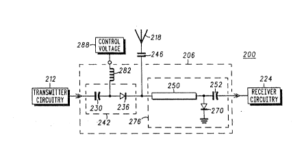
Turning nest to FIG.2, a radio ~e*er, referred to
2~ ge~erally by reference numeral 200 i8 shown. ~adio tra~ er 200
i8 operable ~ a manner similar with that of radio transoei~er 100 of
PIG. 1 a~d illcludes a ~witch circuit, here switch cim~it 206
(compri~et of the~ eleme~ts shown within the block), ~ansmitter
''3 circuit~r 212, tran~ceiYer ante~a 218, and receiver cu~itry 224. .
Switch cîrcuit 206 i0 operable alternately to connect t~namitter
c~y 212 with antens~a 218-or recei~er circuitry 224 vrith
t~am)ceiver aIltenna 218. Switch circuit 206 comprises sene~
coD~ected capa~tor 230 and diode 236 which together fosm fir~t
','3 urcuit path 242, represented by the Uo~ shown irl ~atch Fir~t
"
,,
, .
.,~,!
-12- PCT/U594/0~89
~t path 242, and the ~rcuit elements fo~ Buch, are
analog~us to first ci~t path 142 of radio trsD~3ceiver 100 of FIG. 1.
Capacitor 2~6, analo~ to capacitor 146 of tran~cei~rer 100 of FIG. 1,
o~ a portion of tran~ceiver ~00. i -
8witch circuit 2û6 f~ther compri~es oene~connected
t~mi8~ion li~le 250 alld capa~tor 252 as well a~ diode 270,
po~oIled in a shunt configuratio~ Tra~ ion line 250, capacitor
252, and di~le 270 together form a ~econd ~t path, represented by
blocl~ 276, ~ho~rn in hatch 8econd ~t path 276 and the elements
compri~g such are an~logous to seco~d circl~it path 176 of
t mnscei~er 100 of FIG. 1. C~t path~ Z7G and 176 di~er only i~a that
t~l8mi81~iOn ]i~ ;0 i8 Bllb8titllted for the di~ete elements 148, 158,
and 164 of second Q~it path 176.
Switch circuit 20B filrther in~udes ~ductor 282 which form~ a
radio i~equency choke. A fir~t ~ide portion of i~duztor 282 is
co~nected to first ~t path 24a at t~e node formed between
capacitor 230 and diode 236. A second gide portion of inductor 282 i~
connected to a voltage 8upply, here a control ~oltage repres~ted by
block 288. The ~oltage ~ou~e represented by control ~oltage blo~ 288
and inductor 282 are analogou8 to control voltage block 188 and
induc~or 182 of radio l~ver 100 of PIG. 1.
Opesatio~ of ~witch =t 206 of radio tran~cei~er 200 i~
a~alogou~ with ope2ation of s~vitch circl~it 106 of radio transceiver 100
of FIG. 1, and the detaila of operatio~ of ~t 206 shall not be
descnbed i~ detail.
It ~ould be noted that transmission line 250 i8 functionally
eqwvalent to the combinal;ion of capac~tor8 l58 and 164 and inductor
148 of seco~d c~t path 1176 snd may bei alternately represented by
~uch di8crete compone~ts. Transmis~ion line 250 i8 advaIltage~u~ly
utiliæd ~ place of di~crete component element~ for the reason that a ¦;:
~smisslon line e~ibit~ le~ ertion 108~ the corresponding . -
discrete component elements, and, due to t}le less~r amount of
inseirtion lo88 eshibited by transmi~sion line 250, more ef~icient
opera1ion ofthe ~vitrh c~rcuitii pennitte~i Conventionally,
.
2~ ~ 3 5 7 9 9 r ~
: ~ :WO 94/22531 PCT/US94/02896
13
_
t~nYmi~sio~ line 250 i~ compnsed sf either a conYe~tional ~trip line
or mic:ro 8trip. T~mis~ion li~le 250 is of a le~gth sub~tantially
~s re~pon~g to orle qua~ter the ~aveleRgths of ~ignalB to be
l~aD~nit~ed by ~oeiver a~ten~a 218. (It ahould be noted that
5 1~anami~sio~ line 2~0 fo~ an open ~t at radio f~equencie3 at a
loca~o~ of a length of o~e~rler waYele~gth of the radi~f~equency,
t~nsmi!lsion d ge~erated by ~amlmitter ~y 212 away
f~om the location of a ~hort to ground which here oca:urs when diode
270 folms a ~hort circui~. When diode 270 fonns a ~hort circuit and
1;r~n~mi8~non line 250 fo~ an ope~ ~t at a location of one-
quarter, ~a~el~gth away ~om diode 270, i.e., at t~e side of
t~a~i88101:1 line 250 located away ~om diode 270, tra~5c~iver
na 218 ~comes isolated f~om recei~rer circuitry 224.
However, eve~ thoug~ ~mi~on line 250 iB of a higher Q
Yalue than the corre~ponding dis~ts compo~t~ of 8WltCh 106 of
~IG. 1, a~d, hence, e~ibits a le~ser amount of in~ertion lo~ than do
~he corre~po~g di8crete componen~s of s~Ritch 106 of FIG. 1,
en~onal tran~miss~on lineB al~ ~hibit significa~t amo~-nts of
L~eri;ion lo~e. Accordingly, a rad;o tran~ver~ ~imilar to radio
transceiver 200, including a 8WltCh ~t, similar to switch circuit
206, ha~ing a tra~mission line fo~ a por~on t~ereof, i8 al80
inherenl;ly i~efficient (albeit le88 inefficient than a ~witch c rcuit
comp~ised solely of discrete CO~pOIlent8) due to ~e lar~e amount of
in~ertion lo~ ociated ~vith the element~ of the swi~ Qrcuit.
Turllhg nest to the electrical cir~it ~atic of ~lG. 3, a
prefe~ed embodiment of the prese~t invention i~ shown. FM. 3
illu~atea an electrical circuit schematic of radio transceiver 300 '
which in~lude~ 8~tch ~rcuit 306 compnset of the elements ~hown
within t~e block, t~ansmitter ~t q 312, and recei~er circui~y 324.
Switc}l 306 is operative alternate~ to connect transmitter ~itry 312 '~
to tmn~ver antenna 318 or seceiver circm~ 324 to transcei~rer
ante~a 318. Switch circuit 306, analogous to the ~witch circuits of
the precedi~g figures, indude~ a ~ene~n~lected capacitor 330 and
diod~ 336. Capacitor 330 and diode &~6 t~gether comp~ise first circuit
wos4~22s3lc~,~3~'199 PcTIas94l02as6
path 342 whic~ analogou~ to first circuit path~ 242 arld 142 of the
pl~Cedillg figllre8. Dc bloc~g capscitor 346 i8 ~urther ~ho~n in the
figure a~d i8 a~lalOgOllB to CapaQt4~8 24fi a~ld 146 of the preceding
figures. ,,
Swi~:h ~it 306 furth~r i~clud~ ~eries~nected
tr~mi~sion line 350 a~d capa~tor 352. Cap~Qtor 362 is of a
capacit;iPe value to form a DC bloc~g ca~tor a~d tra~mis~ion
line 350 is of a length substantially r~pondi~g to one quarter the
~a~rele~ of s~gnals to be tran~nitted bg~ tra~oei~er aDte~ 318
and applied to ~ver cu~i~y 324. A~d, ~iode 370 is positioned in a
shu~t ~nfiguration in a manner analogou~ to the po8i~0~ of
diode8 270 and 170 of the preoeding figure8. T~mis~ion line 350,
capacitor 352, and diode 370 t~gether fo~m ~econd cir~it path 376,
repr~ented by the block shown iD hatch~ and which i8 operalble in
manners snalogou~ to the malmer~ in which ~eco~d ~t path~ 276
and 176 of the preceding figure~ are op~r~le.
Switch ~t 306 filrther compnae~ tr~i~gion line 384
ha~ a first side portion thereof conne~ to the node de~ at t~he
coDne~tion be~ween capacitor 330 and diode 336. A ~cond side
portion of transmiasion line 384 i8 coupled to a voltage BOllm, here
o~oe agsin a control voltsge repre~nted by bl~ 388. The control
~oltage i8 a~o isolated from ground by way of capacitor 389.
Applicatio~ of the control voltage to tram~mis~ion line 384 iB
~ectual;ed ~ manners analogous to the application of the control
2~ voltag~ to inductors 282 and 182 of the pr~oeding figa~es.
Iran~iasion line 384 i~ of a length su~stantially corre~ponding to
o~e ~uarter the wavelengths of ~ignals generat~d b~ transmitter
~try 312. Cap~ or 3~9 i8 of a value to form a ~ort circuit to
gro~and at radio ~quencies. Transmis~ion line 384 forms an open l(
~3it at radio ~equenc~e6 at a position located at a distance of one- ¦ -
quarter the wavelength of the radio-i~equeDcg, 1~anemitted 8ig~1al '
gene~ted by tran~mitter circuit 212 a~ay f~om the location of a ~hort
to gro~d. I~nsmission line 384 doe~ t form an open QrCuit for
the dc, control voltage gene~ated by control voltage 388.
2135799
~`~ W0 94t22531 PCTtUS94/02896 ¦`
-15-
Radio tran~ er 300 di~ers wit~ that of radio transceiver 200
of FIG. 2 not oDly due to the substitution of t~;misE~io~ e 384 for
inductor 282, but al80 because tr=is~ion li~le8 350 and 384 are
fonned upon ~3UbstrateB of a oe~e mat~nal rather thsln being
co~pri~ed of oo~entional 8trip line or mi~ strip transrcli~sion
linea. I~an~is~on lines diBpOfied upon ce~c-type mate~al8
eshibit much lower level~ of in~ertion 10~8 tha~ ponding
~is~ioII lines of con~entional ~on~uction. Herlce, radio
trans~iver 300 is in~eren~y more efficient ~an radio transoeiver~
1 0 200 ~ 100 of the preceding figure~.
~ile, in the prefe~d embodime~t of FIG. 3, ~a~mission
lin~38 350 ~d 384 are disposed upon 8 oe~c-t~pe maten~l, the
elemeDts comp~ first and secorld cim~it pat~ 342 8~d 376 may
al80 be disposed upon oIle or more ceramic substrate~.
1~ Turning ne~t to the schematic ~ew of P~G. 4, a switch ~t,
her~ refened to generall~ by 2~fereDce ~umeral 406, of a preferred
embodi~nt of the present in~e~tio~ ho~n in ~ natic fon~L
SwltCll ~t 406 i8 equiYal~nt to 8wits~ circuit 306 of ~IG. 3 wherein
many of tha elements compr~8~ng first and ~econd circu~t path~ 342
s~nd 376 are al80 (ln sddition to ~am;mission ]ines 350 and 384)
disposed upon ceramic-type sub~tratss. Ill ~he ~mbodimeIlt of Pl~. 4,
~witch 406 iB comprised of sis tandemly-position~d oeramic
~ub8trate~. Tra~mi~sion line~ 350 and 384 and the component
eleme~t8 of first and second circuit pat~s 342 and 376 sre ~;sposed on
~ou~ one8 of the ~ub~trates.
Top ceramic substrate 390 i~ oned abo~re second ceramic
sub~trate 391 which, in tu~, i~ positioned above third ceramic
~ubstrate 393. I~ird cersmic sul~strate 393, i~ ~, is positioned
a}~o~e fourt~ C8ramlC ~ubstrate 395, which, in tur~, i8 poBitioned
above fi~ cer~c 8ubBI rate 397. P~ ~ramic sul~strate 397, in
tu~, i~ positioned abo~re bottom ceramic ~ trate 399. ~;
Variou~ portion~ of vanou~ of the component element~
cor~ponding to first a~d second ~t paths 342 and 376 and
t~llml88iO~ line 384 of ~wit~ cu~nt 306 of radio tra~soei~er 300 are
W094/Z~53~ 3S~199 PCTmS94/0~896 ~ jL,
- -16-
disposed upon variolas one~ of ce~c ~ubstrat~ 390-39g. Vi R
formed of path~ of oonductive material e~ding thro~ potion~ of
~anous one~ of the cera~c ~Btra~B 3~399 pe~it intercormec~on
between component~ di~po~ upon ~anous o~es of the ~ub~rates 390-
399. Di~rete diode~ ~prefe`rably PIN-~pe diode#) 401 and 403 are
mou~ d upo~ the top ~u~e of first cs~c subst;rate 390. Diodes
401 and 403 correspond to diod~ 336 and 3?0 of EIG. 3. Onc~ the
ceramic substrates 39~399 are ta~deml~ ~it;io~ed in the deiiired
arrangement sho~ i~ the figure (and diod0~ 401 and 403 are
1 O mounted upon fillbStrate 390), the pl~ty of tandemly-po~i~o~ed
Bllb8trat~B are ~ed (i.e., t~e oeramic ~1~8trate~ are baked in all o~en)
for a period of ~me, thereby to form a ~d Rt~u~e of the plurality of
oeramic ~ 390-399.
I~ning ne~t to the plan ~iew of PIG. ~1, the top ~urface of
ce~c sub~trate 390 is ~how~ C~atings of el~c~ic~lly-co~lduclive
~atexial disposed upor- the top ~ ~ur~ce of oera~ic Bllbfitrate 390
are indicated by ~c~ons of $he filce ~ce shown by hatch
mar3~ga A~ illusl~ted, three pad~ 412, 414, a~d 418 are di~posed
upo~ the top faoe ~ur~ce of ce~c sub~ e 390. Top ends of ~
420, 422, a~d 426 are positioned ~nth~n respective o~ea of pad~ 4l2418.
Pad~ 412 and 414 form mounti~g location~ permitting mounting of
diode 401 (~hown in FIG. 4) ther0upon, and pad 418 fo~ a mountin~
loca~o~ pe~tting mountirlg of diode 403 (also ~hown in FIG. 4)
t~ereupon. A second ~ide of diode 403 i8 ~lted upon the face
~urface of ~ub~ e 390 which i~ coated ~ith the coa~g of tbe
e~ectrically-conductive material and w~ich defi~les a ground plane.
Top ends of ~ia8 420 aDd 422 pe~t co~nection of diode 4:01, onoe
unted ~ po~i~o~ upon!pads 412 s~d 414, to ot~r ciDi~y dispo~ed
upon o1~ers of the oera~c sub~trates 391-399. ADd, na 426 perrnits
con~ o~ of diode 403, once mouDted i~ ition, to circui~
disposed UpO~I OthBrll of the oeramic plat~ 391-399.
FIG. 5-2 is a plan ~iew of t~e top BU~Ce of secorld cer~mic
~ubst;rate 391. Similar to the preceding figure, coatings of oonducti~e
mate~al formed upo~ the top filce ~ce of ceramic 3ubstrate 391
~135799
. -WO 94/Z2531 PCT~US94/02896
- ~7 --
are ~dicated by hatcb markings. Serperl~like path~ 550 ~nd 584
are formed upon ~he ~ce surface of se~ d ~ trate 391. Such pa~h6
form t~mi~sion liDB8 analOgOIl~ to transmis~ion li~es 350 and 384
of switch ~it 306 of ~lG. 3. LeDgth~ of each of th~e pat~s 55Q and
~84 ~ ally corre~pond to len~ths of o~e qlaarter the
wavele~s of signal~ to be t~itt~d b~ a tran~iver
~rpor~ng ~wit~ ~t 408 of which paths ~0 and 584 form
porlions. (B~ proce~ of e~penma~at;iorl, ~tio~ i~ the ~ctent of
the ~e~pentin~like shape of ~he ~an~iaE~o~ lillefi c8u~e Blîght
v~ance in the characteri~tic8 thereof; ~uch ~an8tiOIl may alter
slightly the performance of the ~t 80 fo~med.)
Top e~ds of via~ 586, 588, 590, and 592, which e~tend through
~ubsl*~dte 391 are also ~h4wn in tbe ~e. Via 686 i~ positioned to
pe~t ali~ment ~vith via 422, na 588 i8 positioned to permit
alignment ~ith ~ia 426, Qntl ~ria 590 i~ po~i~oned to pe~t alignmeIlt
with na 420. When oe~c sllbsb~ltes 39û a~d 391 are ali~ed with
one another and tandemly~ tio~led theratogether, an eIld portion of
path 584 become~ electrioally connectsd ~ diod~ 401 mounted upon
psd 412 of subgtrate 390, a side portion of path 550 i6 8imilarly
~ ected to diode 401 mountsd upon pad 414, and a second ~de
por~on of path 550 is connectet to ~iode 403 mou~ted upon pad 418.
A~ noted prenously, for~on of transmiB~ioIl line8 formed of paths
650 a~d 584 upon a oeramic ~ trate i8 ad~a~tageou~ a~ the
insertion 1088 of transmi8~iOn lines s~formed is ~ificantly low~r
than the i~sertiO~ 108B of conventional, ~an ;miB~iOn lines formed of
strip linea s~d micro stripB.
~IG. 5-3 i~ a plan ~iew of a top faoe Aur~ce of ceramic ~ubstrate
393 of switc~ ~it 406 of ElG. 4. Only top end~ of ~ias 6~;0, 6~2, 6~
and 666 are disposed upon the top face BU~Ce of ceramic ~ubstra~e
393. And a ~ubstanl;ial portion of tile ramainder of t~le fsoe ~ur~ce i8 ~-
coatsd ~it~ the coating of elec~icallg-conducti~e material but for ~.
~mall i801ation srea~ P0Biti0ned about t~e top er~ds of ~1ia8 650-6B6. ~,
Becau~e of the coating of ~ec~ically conducti~e material dispo~ed `
upon subAtrate 393, BUbl~t~ate 393 fonn~ a~ isolation pla~e for :
i~ola~ paths 550 and 584 which form t~nsmis~ line~. Via~ 6Bt)- ~
W0 94/2~;31 3S~ 9 9 -18- PCTl S94/0;!896
656 se~re merely to interconnect re8pe~ve on~ of the ns~ 424, 586,
588, a~d 5~0 (and the a~so~ated element~ co~ected to BUch ~ to
ci~nt eleme~ts dispo~ed upo~ other~ of ~e ~ trates 395-399.
P IG. 5 4 i8 a plan ~ew of a top ~ ~e of ceramic 8ub~trate
390. Agai~, portio~ o~the top ~ ~e of ~ trate 395 coated
with th~ coa~ng of the ~lectri~y~o~ ve materisl are indicated
by hat~h ~rl~gs in t~e Sglre. ~ iLlustrat~ four pad~, ~amely
pad~ 730, 7~2, 758, and 789 are fo~d upo~ ~e f~ urface of
~ub~ 395. Each of the pads 730-789 form plate8 of ca~l;ors
whi~ corr~spond to plates of ~tors 330, 352, 358, and 38!3 of
switch circuit 306 of PIG. 3. Top e~ds of via~ 791, 793, 7~5, and 797 are
how~ in the figure. Via 791 i~ po~tioned to per~t ali~ment
with via 650, ~a 793 is po~o~d t~ ~t aligDmel~t with via 656t ~ria
795 i~ itio~d to ~t iligDment with ~ 652, and vis 797 i~ ~
it;iollsd to per~t a~eDt ~th ~na 654.
PIG. ~5 i~ a pl~ ~e~, ~imilar to t~o8e of the precedi~g four
figl~eB, but of a top f~ ce~c ~ubstrste 397. A$ain,
~oa~g~ o~ the el~c~ically coDductiv~ material coa~d upon portions
o~the ~ Bl~Ce of ~ubstrate 3g7 are ~dicated by hat~h Jnar]~gs.
A~ illu~trat~, pads 830, 8~2, 858, and 897 are formed upon t~ oe
811~Ce of 8ub~ttat8 397. Top ~ of ~8 890, 892~ 894, and 896 are
hown in the figure. Analogous to plate member~ 730-789
dispo3ed upon t~e f~oe ~ur~oe of ~ub~trate 395, pads 83~899 dispo~ed
upo~ ~e f~oe ~fa~e of BUb~ate 397 also form plat~ members of
capacitor~ corre~pondi~g to capaeitors 330, 352, 358, aIld 389 of B~itCh
~t 308 of FIG. 3. It ~hould be noted t~ vias 890-896 ar~
po~oIled t to alig~ with ~ 791-7S7 and are slec~ically i~olated
t~er~m. Thereby, plate msmber~ 730 a~d 830, 7~2 and 852, 758 and
858, and 789 and 889 E~ intaj~ed in is~olation ~om oD~e a~other,
t~ereby to fo~n oppo~ ~ides o$ capacitor~
It ~hould be rlotsd that ~riatios~ e ~ of the plate~ of the
capacitor~ permits vanance in th~ capacili~e ~alue~ of the capacitors
fo~m~d of ~u~ p~ates. Capa~to~s of ~e~ larger ~alues may be
fonned by positi~ ~luralitie~ ub~trateB whe~in t~e pluralil;ie~
W0 94/22531 21 3 5 79 ~ PCT/U594/02896 ;~'
-19-
of pla~&~ are po~itio~ed in parallel connec~ . (Use of additio~
number~ of ~ubst;ratsa would, of cour~ use the filter ~t to be of
a g~ter ~ lS8.)
~lly, t~ing to ~IG. ~6, a top f~ce sur~ce of ceramic
Btlb~ate 399 i~ ~hO~L AgaiI~, porlio~ of the f~ ur~ce of the
~ll~Btrate Cl~ated ~th th~ coati~lg of el~ically-co~ducti~e material i8
i~dica~ed by hatch mf~rkj~, Four pad~, ~mel~r pad~ 950, 952, 954,
and 9~6 are disposed u~on the ~p f~ ~e of sub~trate 39g. Other
portio~ of the ~e of ~ ;rate 399 ar~ o coated with the
c4a~g of ~lec~cally~ducti~e ma~rial, but i~olated f rom pad~ 950-
956 b~ on ares~ ~bout the pads. Top ~ ~ g9t), 992, 994,
and 99S are a1BO iIlu~ated~ Pad 960 ~ta connec~on to
tr~mitter ~rcuitr~ uch as ~mitter circui~y 312 of :radio
tran~cei~er 300 of PIG. 3). Pad 952 ~b co~ on ~o a
1~ tra~ceiYer a~ n~ (8UC~ a~ver a~t~ 318 of radio
t;rsn~ce~Yer 30û of FIG. 3), pad 954 ~t~ connec~o~ ceiver
circuitry (BUt:h a~ sr circuitr~r 324 of transc~Yer 300 of ~IG. 3),
a~d pad 956 permit~ on ~t~ a~ e~l, bias ~oltage. Via
990 ~ po~ med to permit ali~ment ~it~ ~ia 890 of substrate 337, ~a
99~ is poe~itioned to pennit alig~ent ~ith Yia 894, via 992 i$
po~i~o~ed to permit alignment witb ~ia 892, aDd ~ 996 i8 positioned
to pesmit alignment with ~ia 896. Hence, by ~uitably comlecting
transmitter snd receiver circuil;ry to pads 950 and 994, re~ vely, a
tra~ver antenna to pad g52, and by appl~ a control ~roltage to
pad 956, a circuit similar to the circuit of radio tran~ceiver 300 of FIG.
3 ma~ be form~d~ -
By s~tably aligni~lg of 8Ub8tratB8 390-399, pO8itiO~lllg the
~UbBtrat~ 390-399 i~ ta~dem, i~ring t~e s~bstrates, and po~itionin~,
8U~}1 a8, e.g~, ~ soldering, diodes upon mou~ti~g pads 412-418 of top
substrate 390, a ~n~ Qrcuit correspondi~g to ~witch cu~ uit 406 of
~IG. 4, may be fo~ned. I~ a prefened embodiment, after firing of the ~.
substrates, t~e switch circuit i8 of a h~ighth o~ appro~tely thir~-
sne mil8. B~cause the swit~ circuit es~libits mu~:h less i~sertion
lo~ th~ 8witch circui~s of con~entionsl cor~truclio~ use o the
WO 94/22531 PCT/US94/02896 ;
213~799
- -20 -
switch circuit of the preferred embodime~ e pr~ent inve~on
permits a radio tra~sceiver, 8UC~ a c~llular ~adiotelephone
operable. . . , ~:~
While the pre~t i~ventio~l has bee~ ~8~8d in c~ on
wi~ the preferred embodi~t~ showD in t}le ~ous figure~, it i~
be und~rstood that other ~imilar embodiments may be u~ d
modific~ons and addi~on~ may be made to th~ de~bed
embodime~t~ for perf~ the ~ame ftanctioII of the present
inven~on without deviating there~m. Therefore, the pre~ant
inven~on 3hould ~ot be ~t~d to a~y ~ingle embodimellt, but rather
constru~d in breadt~ and ~cope in accordance with the recitation of
the appended claims~
.
,
:.