Note: Descriptions are shown in the official language in which they were submitted.
213~982
-
LATERAL BIPOLAR TRANSISTOR
FIELD OF THE lNV ~:N-'~ ION
This invention relates to a lateral bipolar
transistor and a method of making a lateral bipolar
transistor for an integrated circuit.
RA~R~ROUND OF THE lNV~N'~ ION
In fabrication of silicon semiconductor based high
speed integrated circuits, the integration of both CMOS
(complementary metal oxide semiconductor transistors) and
bipolar transistors to provide Bipolar-CMOS (siCMOS) VLS
integrated circuits is now well established for
telecommunications applications requlring high speed, high
drive, mixed voltage and analog-digital performance.
However, there is considerable challenge in optimizing the
performance of both CMOS and bipolar devices for integrated
circuit fabricated with progressively reduced dimensions.
A manufacturable fabrication process for mi ni mnm geometry
integrated circuits must be provided without inordinately
increasing the process complexity, i.e. the number of mask
levels and process steps.
Bipolar transistors having an emitter-base-
collector structure in either a vertical or a lateral
configuration are known. Key parameters that must be
reduced to increase switching speed are base width, base
transport time, base resistance and base-collector
capacitance.
In combining shallow junction CMOS transistors
with bipolar transistors for a sub-micron BiCMOS VLSI
integrated circuit, a vertical bipolar transistor is
commonly used. For example, a vertical PNP bipolar
transistor comprises a buried collector formed in a P type
region of the substrate, a heavily N doped base region is
3s provided in the substrate surface and an heavily P doped
emitter region overlies an active base region, forming an
emitter-base junction. Base contacts are provided to the
2135982
-2
base region of the substrate surface adjacent the active
base region. Contact to the buried collector is made
through a heavily P doped region (i.e. a sinker) extending
to the substrate surface. A vertical bipolar transistor
with a shallow base width may be obtained in a process
compatible with forming shallow junctions for CMOS
transistors. For example, a bipolar transistor with a base
width of -0.2~m may be achieved by low energy ion
implantation, or by diffusion of impurities from an
0 overlying heavily doped layer.
On the other hand, a conventional lateral bipolar
transistor differs in structure considerably from a
vertical bipolar transistor. A typical PNP lateral bipolar
transistor comprises a substrate on which is formed a P
- 15 doped epitaxial layer. Heavily P doped regions are defined
in the epitaxial layer to form an emitter and a collector.
The latter are defined by ion implantation of surface
regions. The active base region is provided by the N doped
layer disposed between the emitter and the collector-, the
base width being defined by the lateral spacing of the
emitter and the collector. A buried base contact is
provided by an underlying heavily N doped base electrode
region. Thus, in a lateral bipolar transistor of this
structure, the base width is constrained to be larger than
or equal to the m; nl mllm photolithographic resolution used
in defining the implantation area for the emitter and
collector regions. As an example, in a BiCMoS integrated
circuit formed by a 0.8~m process, the base width of a
lateral bipolar transistor would be ~4 times larger than
the 0.2~m base width typically obtained in a vertical
bipolar transistor.
Furthermore, a conventional lateral bipolar
transistor suffers poor efficiency because, when the
emitter-base junction is forward biased, carriers are
launched in all directions from the emitter, not only
towards the emitter, but also towards the substrate. In
the layout of a conventional lateral transistor the
2135982
collector is annular and encircles the emitter to improve
the collector efficiency.
Various schemes have been investigated to improve
the performance of lateral bipolar transistors, for
example, as discussed in U.S. Patent 5,081,517 to Contiero
et al. (SGS-Thomson-Electronics) issued 14 January 1992
entitled mixed technology integrated circuit comprising
- CMOS structure and efficient lateral bipolar transistors
with a high early voltage and fabrication thereof". In a
0 large dimensional lateral bipolar transistor, i.e. in a low
density integration, the collector and emitter extend
relatively deeply into the well region and the emitter
current is efficiently collected by the collector.
However, if a lateral bipolar transistor is integrated with
a shallow junction MOSFET, and has a correspondingly
shallow collector region, the collector efficiency may be
very poor. In the lateral bipolar transistor of Contiero
et al., a collector "extension~ region of the lateral
bipolar transistor is provided. The latter extends
relatively deeply into the well region compared with a CMOS
junction region, to intercept the emitter current and
gather it to the collector, and thus improve collector
efficiency. An annular diffusion region provides a
collector which encircles the emitter region and thus
increases the collector efficiency, and further reduces the
proportion of the emitter current which is lost to the
substrate.
In another approach, it is known to form trench
based lateral PNP bipolar transistors in which an emitter
is provided by a sidewall of a trench to increase the
injecting area and provide a more efficient cross-section
for a high performance PNP. For example, a method of
forming higher performance lateral PNP transistor with
buried base contact is described in U.S. 5,198,376 issued
30 March 93 to Divakaruni et al ~IBM). However, provision
of trenches adds to the number of processing steps, and the
2135982
,
process is not as readily integrated into a BiCMoS process
including shallow junction CMOS transistors.
SU~lARY OF THE INVENTION
Thus the present invention seeks to provide a
lateral bipolar transistor structure, an integrated circuit
including a lateral bipolar transistor and method of making
a lateral bipolar transistor structure which overcomes or
reduces the above mentioned problems.
0 According to one aspect of the present invention
there is provided a lateral bipolar transistor for an
integrated circuit, comprising: a semiconductor layer of a
first conductivity type formed on a substrate; first and
second heavily doped regions of a second conductivity type
defined in the surface of the semiconductor layer and
laterally spaced apart, said first and second heavily doped
regions defining an emitter and a collector respectively of
the lateral bipolar transistor; an active base region of
the bipolar transistor comprising part of said
semiconductor layer disposed between said emitter and
collector, the active base region comprising at least one
layer of a semiconductor alloy having a predetermined
valence band offset relative to the heavily doped regions
forming the emitter and the collector.
Thus a heterostructure lateral bipolar transistor
is provided having a base region comprising an alloy
material which provides a predetermined valence band
offset. The base region may comprise e.g. a relatively
narrow band gap material. The resulting band structure
enhances transport of carriers from the emitter to the
collector in a lateral manner through the alloy layer and
increases lateral gain of the transistor. Advantageously,
during operation, the hetero-offset results in the emitter-
base junction, i.e. between the emitter and the alloy
layer, being more strongly turned on and therefore
injecting carriers into the alloy layer, and reducing
injection of carriers in a direction away from the
2135982
collector. Furthermore, carriers not emitted into the
alloy layer tend to be drawn towards it by a strain field
associated with the lattice mismatch between the
semiconductor and the alloy layer. For example, where the
semiconductor layer is silicon, and the alloy layer
comprises a silicon-germanium alloy, SixGel-x~ the
composition of the alloy controls the band offset and
presence of germanium in the alloy layer increases minority
carrier mobility. Thus, the value of x may be selected to
o provide a predetermined band offset to control the
characteristics of the resulting transistor.
Alternatively, the base region comprises a
superlattice structure, for example, provided by a series
of alternating thin layers of Si and SiGe alloy. By using
a superlattice structure, the band gap structure may be
tailored, to provide a desired band offset.
Correspondingly, the band gap offset of the superlattice
layers enhances carrier transport through the base region
and mitigates problems with poor collector efficiency found
in a conventional silicon based lateral bipolar transistor.
According to another aspect of the present
invention there is provided an integrated circuit
comprising a silicon heterostructure lateral bipolar
transistor. Advantageously, the transistor is formed on a
silicon semiconductor substrate and has a base region
comprising a silicon-germanium alloy disposed between an
emitter region and a collector region provided by laterally
spaced apart regions comprising heavily doped silicon.
According to yet another aspect of the present
invention there is provided a method of forming a lateral
bipolar transistor comprising: providing an integrated
circuit substrate having a having a lightly doped epitaxial
semiconductor layer formed thereon of a first conductivity
type; providing therein first and second heavily doped
regions of a second conductivity type defining an emitter
and a collector respectively; and providing in a region
disposed between the emitter and the collector, an active
2135982
base region comprising a layer of a semiconductor alloy
providing a predetermined valence band offset.
Processes for forming the lateral bipolar
transistors may be provided by steps compatible with known
bipolar CMOS processes. Where the narrow band gap
semiconductor alloy layer comprises a silicon germanium
alloy, the latter may be provided by epitaxial growth in a
method compatible with conventional CMOS process
technology. Alternatively a silicon germanium layer may be
provided by germanium implantation and annealing of a
silicon layer. Where a base region with a tailored band
gap structure is to be provided by silicon superlattice
structure, e.g. a series of alternating very thin (loA to
30A thick) layers of silicon and silicon germanium alloy,
the latter may be deposited by suitable known methods,
e.g., molecular beam epitaxial (MBE) growth.
Thus an improved lateral bipolar transistor, an
integrated circuit including a silicon heterostructure
lateral bipolar transistor and a method of forming a
lateral bipolar transistor are provided, ln which the above
mentioned problems are avoided or reduced.
BRIEF DESCRIPTION OF THE DRAWINGS
Embodiments of the invention will now be described
by way of example, with reference to the accompanying
drawings, in which:-
Figure 1 shows a cross-sectional view of part of a
conventional prior art integrated circuit including a
lateral bipolar transistor and CMOS transistors;
Figure 2 shows schematic cross-sectional view
through a lateral bipolar transistor comprising part of an
integrated circuit according to a first embodiment of the
present invention;
Figure 3 shows an energy band diagram for the
transistor of the first embodiment in the plane through the
emitter-base-collector;
2135982
Figure 4 shows an energy band diagram in the plane
from the active base region from the surface through the
substrate of a transistor according to the first
embodiment;
Figure 5 shows schematic cross-sectional view
through a lateral bipolar transistor comprising part of an
integrated circuit according to a second embodiment of the
present invention;
Figure 6 shows an energy band diagram in the plane
0 from the active base region, extending for the surface
through the substrate, for a transistor according to the
second embodiment; and
Figure 7 shows a circuit diagram of a class AB
complementary emitter follower output stage to illustrate a
typical application of NPN and PNP lateral bipolar
transistors according to the first embodiment of the
present invention.
DESCRIPTION OF THE PREFERRED EMBODIMENT
Part of a known prior art BiCMOS integrated
circuit 10 formed on a semiconductor substrate, i.e. part
of a silicon wafer 12, is shown in Figure 1. Openings
through a field oxide layer 14 define device well regions
of the substrate, in which are formed a conventional PNP
lateral bipolar transistor structure 16, and conventional
CMOS transistors 18 and 20. The lateral bipolar transistor
16 comprises and emitter region 22, an annular collector
region 24 surrounding the emitter 22, and a buried base
electrode 26 with a base contact 28 at the surface. When
current from the emitter 20 is launched in all directions,
as shown schematically by the arrows, although the annular
collector 24 surrounds the emitter 22, a significant
proportion of the current may be lost to the substrate.
Consequently, the lateral bipolar transistor efficiency is
poor.
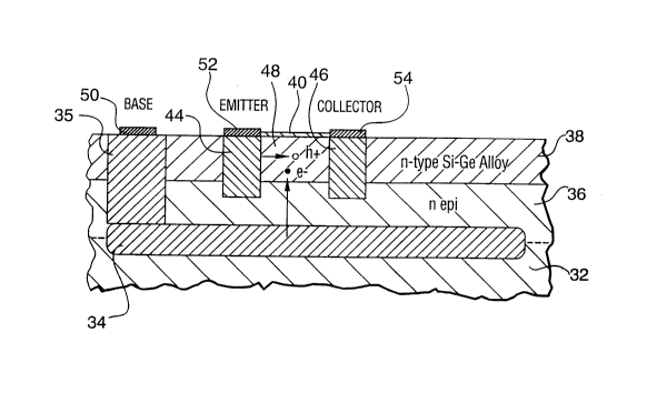
A lateral bipolar transistor 30 comprising part of
an integrated circuit according to a first embodiment of
2135982
the present invention is shown in Figure 2. The transistor
30 is formed on a silicon substrate 32, e.g. a conventional
silicon semiconductor wafer, shown in part in figure 2,
having an overlying layer 36 of lightly N doped silicon,
about 1 to 3 ~m thick, and in which is selectively defined
heavily doped N+ and P+ buried layers. The latter layers
are incorporated in a manner conventional for BiCMOS
integrated circuit manufacturing. Figure 2 shows a N+
doped buried layer 34 only. Overlying the lightly doped
silicon layer 36, there is provided about 500A-2000A of a
layer 38 of lightly N doped silicon germanium alloy, that
is, Sil_xGex~ with 0<x<1, the composition being selected to
provided a predetermined band gap offset, dependent upon
the specific design of the transistor as will be discussed
below. Spaced apart, heavily doped P+ doped regions are
defined in the surface region extending through the Sil_xGex
alloy layer to provide an emitter 44 and a collector 46 of
the transistor 30, and so that an active base region 48 of
the transistor is provided by the Sil_xGex alloy layer
extending between the emitter 44 and collector 46.
Overlying the silicon germanium alloy layer 38 is provided
a thin layer 40, about 50-300A thick, of dielectric, i.e.
silicon dioxide. The latter also serves a gate oxide, e.g.
in a CMOS portion of a BiCMoS integrated circuit (not
shown). The resulting structure thus forms a silicon
heterostructure lateral bipolar transistor 30 to which
contacts 50, 52, and 54 to the base, emitter and collector
respectively are provided.
The Sil_xGex layer results in a hetero-offset in
30 both the conduction and valence bands relative to the
substrate when grown commensurately on the silicon
substrate (i.e. using the same lattice constant as silicon)
The magnitudes of these band offsets are dependent on the
fractional Ge content of the Sil_xGex alloy.
Representative energy band diagrams are shown in figures 3
and 4, in which the Evand Ec are the valence band energy and
conduction band energy, respectively. Figure 3 shows the
2135982
-
band diagram in a plane extending laterally through the
emitter-base-collector. Figure 4 shows the corresponding
diagram in a vertical plane from the surface through the
active base region to the substrate.
The band alignment of strained Si1_xGex to silicon
is Type I, with most of the hetero-offset incorporated into
the valence band. For example, for x =0.25 the conduction
band offset, ~Ec = 0.02eV and ~Ev = 0.185eV (e.g. see
reference by R. People, ~Physics and applications of
o strained layer heterostructures~, IEEE J. Quantum Electron.
vol. 22 pp.1696-1710 (1986)).
The incorporation of the Si1_X Gexlayer in the
active base region between the emitter and the collector of
a lateral bipolar transistor enhances the carrier transport
in the base and enhances the gain in a manner analogous to
an conventional heterojunction transistor, i.e. a vertical
configuration hetero-junction bipolar transistor (HBT)
which comprises for example, a silicon-germanium base or
silicon carbide emitter structure.
In a heterojunction transistor, the gain ~is
proportional to Ne/Nb exp (~EV/kT), where Nb and Ne is the
doping in the base and emitter respectively. With larger
~Ev, the gain increases exponentially.
The base transit time ~b = Wb2 /2Db where Wb is the
base width and Dbis the diffusion constant for the alloy.
Figure 3 illustrates the energy band diagram from
the emitter to the collector along a plane which intersects
the Si1_X Gex layer for the transistor of the first
embodiment. This diagram is similar qualitatively to that
30 for a conventional HBT however, it must be appreciated that
in the lateral bipolar transistor described above, the
transport enhancement comes about as a result of the
presence of Ge which increases hole mobility and therefore
diffusion across the base. Implanting and annealing the
emitter region of the structure disorders it, relieving
strain and broadening the Ge content, so that the emitter
is composed of wider bandgap alloy. In addition, in
213S982
-
operation of the transistor, the junction between the
emitter and the base is turned on more strongly at the
interface between the large and small bandgap material thus
reducing injection which is not coplanar with the
collector. Thus overall emitter efficiency is improved.
Even carriers not injected directly into the Si1_X Gex layer
will be drawn towards it by the strain field associated
with the lattice mismatch between the alloy and the
substrate layer. That is, growing a Si1_X Gex layer
0 commensurately, i.e. so that it matches the underlying
lattice of the silicon substrate layer at the SiGe/Si
interface, tetragonally distorts the crystal. In the plane
of the interface on the alloy side, the atomic positions
are compressed and on the silicon side they are expanded.
Perpendicular to the interface on the alloy side the atomic
positions are in extension compared to the bulk alloy. On
the silicon side they are compressed. This distortion on
both sides of the interface results in a strain field which
draws holes towards the valence band energy well of the
Si1_X Gex layer.
In effect, as a result of the valence band hetero-
offset there is a net diffusion of holes from the silicon
to the Si1_X Gex layer. Diffusion in the opposing direction
is inhibited by the energy wall at the interface.
Clearly, placing a layer of Sil_xGex alloy in the
plane linking the emitter and collector of a lateral PNP
transistor has a number of beneficial effects on the
performance of the device:
larger lateral gain as a result of hetero-offset.
enhanced minority carrier transport (higher
mobility as a result of the incorporation of Ge
in the layer.
improved emitter efficiency because the emitter
base junction turns on more strongly at the
interface between the wide bandgap emitter and
narrow bandgap base.
2135982
-
11
A lateral bipolar transistor 60 comprising part of
an integrated circuit according to a second embodiment is
shown in Figure 5. The lateral bipolar transistor 60 is
formed on a semiconductor substrate 62 having an overlying
lightly n doped epitaxial layer 64, and including a heavily
n doped buried layer 66, similar to that of the first
embodiment. However subsequent layers of the structure
differ from the first embodiment in that the layer
providing the base region , instead of comprising a single
o Si1_X Gex alloy layer, is provided as superlattice structure
70 comprising a single or multiple series of thin
alternating layers 72 and 74 of Si1_X Gex and Si (Figure 5).
The superlattice structure 70 of the base region can be
fabricated to provide an arbitrary band structure, in this
case providing a hetero-offset in both the valence band and
conduction band relative to the emitter and collector
regions as shown in Figure 6. The required band structure
is accomplished by designing a superlattice structure
comprising a series of alternating thin layers of a
semiconductor alloy and a semiconductor, i.e. Si1_xGex and
Si, the thicknesses of the layers in a superlattice
structure and their composition controlling the band
structure and offsets, and the series of layers being
selected to provide predetermined valence band and
conduction band offsets, as required. A surface layer 76
of silicon is provided over the superlattice layers.
Heavily doped regions forming an emitter 78 and collector
80 are defined by ion implantation, as described in the
first embodiment. The collector and emitter extend through
the layers of the superlattice structure, and an active
region 82 of the base is thus provided by that part of the
superlattice structure extending between the emitter 78 and
the collector 80. A thin gate dielectric layer 84 is
provided on the silicon surface between the emitter and the
collector
The superlattice layers 72 and 74 are very thin,
~10 to 150 A, and thus incorporate quantum effects. The
2135982
band structure of the active base region provides enhanced
minority carrier transport lateral through the base,
similar to the effect in the transistor according the first
embodiment. Quantum confinement effects in superlattice
structures include discretization of the hole energy
continuum, and hole mobility enhancement, effects which are
well understood and described in the literature pertaining
to reduced dimensionality structures.
Such thin layers of a semiconductor alloy may be
grown without doping. Advantageously, the resulting
transistor does not suffer base-width modulation, i.e. the
Early effect, found in a conventional lateral transistor.
Furthermore, undoped layers may have higher mobility
because ionized impurity scattering is reduced.
In the transistor of the second embodiment,
structure advantageously, a gate electrode (not shown) is
provided overlying the surface silicon layer 76 between the
emitter and collector , and separated therefrom by the thin
dielectric layer 84, the latter thus acting a gate
dielectric. The purpose of the gate electrode is to
destroy the MOS channel which exists in the surface region
76 of the base linking the emitter and the collector, which
would otherwise result in a surface leakage current.
Whether or not a gate is necessary depends on the doping in
the structure, and the resulting subthreshold current. By
tying the emitter to the gate, thus turning off the surface
MOSFET i.e. by controlling inversion in the channel region
underlying the gate, surface leakage may be reduced.
The use of a gate electrode in a lateral bipolar
transistor is described in more detail in co-pending U.S.
Patent Application to Duljit Malhi et al, filed
concurrently herewith.
Although the embodiment described above relates to
an pnp transistor, npn transistors may be fabricated
correspondingly using elements of opposite conductivity
type. A circuit diagram illustrating a typical application
in a class AB complementary emitter follow out put stage of
2135982
npn and pnp lateral bipolar transistors Q1 and Q2, is shown
in Figure 7
Transistors according to the first or second
embodiments may be fabricated by methods compatible with
conventional processes for fabrication of bipolar, and
bipolar CMOS integrated circuits.
For example, in a method of forming the transistor
30 according to the first embodiment, a silicon substrate
32 is provided having a lightly doped N layer 36
0 epitaxially formed thereon in a conventional manner. A
heavily doped buried layer 34 is then formed in a
conventional manner, i.e. by selectively masking, by
coating with photoresist and patterning, followed by ion
implantation and annealing. A layer 38 of silicon
germanium alloy is deposited on the substrate by a known
method, e.g. by epitaxial growth of a silicon germanium
alloy, or by formation of a layer of silicon followed by
ion implantation of germanium and annealing. The silicon
germanium layer 38 is provided having a composition
Si1_xGex~ the value of x being selected to provide a
predetermined conduction band and valence band offset
relative to the substrate as described above.
Subsequently, emitter 44 and collector 46 regions are
defined by ion implantation with a heavy dose of P type
dopant. A contact to the buried layer 36 is provided, in a
conventional manner, through a heavily doped region 35
which extends down through layers 38 and 36 to contact the
heavily doped buried region 34 which forms the buried base
electrode. The latter heavy implants are preferably
annealed by rapid thermal processing to avoid unwanted
diffusion in the Si1_xGex alloy layer. Electrically
conductive contacts 50, 52, and 54 to the base, emitter and
collector electrodes respectively are provided by
conventional known processes.
Thus a lateral bipolar transistor according to the
first embodiment may be provided by a method which is
2135982
-
compatible with known VLSI processes for forming bipolar,
CMOS and BiCMoS integrated circuits.
In other methods of fabricating a silicon
heterojunction lateral bipolar transistor according to the
first embodiment, may include alternative methods of
forming the germanium silicon layer, e.g. as described in
~A method of forming a germanium layer and a HBT" Verret et
al. in U.S. Patent 5,089,428, issued February 18, 1992.
In successive steps of forming a transistor 60
0 according to the second embodiment, a substrate 62 is
provided in the form of a conventional silicon
semiconductor wafer, having a lightly doped N layer 66
formed epitaxially thereon. A heavily N+ doped layer 64 is
formed in a region of the substrate, e.g. by ion
implantation, to provide a buried base contact electrode in
the substrate. Layers 72 and 74 forming the superlattice
structure 70 are then deposited or grown epitaxially on the
surface of the epitaxial layer to form a heterostructure
including alternating thin layers, of lightly N doped
silicon 74 , a layer of a silicon germanium alloy 72, and
another layer of lightly doped n type silicon 74. These
layers 72 and 74 are deposited or grown epitaxially on a
clean surface of the silicon substrate by any suitable
known method, for example, UHV-CVD (ultra high vacuum
-chemical vapor deposition) MBE (molecular beam epitaxy) or
rapid thermal CVD.
A field isolation layer, e.g. an oxide layer, is
provided selectively on the N silicon surface, by a known
method, to define device well regions. A contact is
provided from the surface to the buried N+ layer. The
latter may be provided by ion implantation after
selectively masking the surface with photoresist, thus
forming of a heavily N+ doped sinker region 65. After
stripping the implant photoresist mask, an oxidation step
is performed to provide a thin layer of gate oxide. Then a
polysilicon layer is deposited overall for defining gate
2135982
electrodes of field effect transistors, and if required, a
gate electrode for the lateral bipolar transistor.
First and second heavily N doped regions defining
an emitter 78 and a collector 80 of bipolar transistors are
5 then formed by ion implantation of a suitable N dopant,
e.g. phosphorus ions, followed by annealing. Annealing is
preferably accomplished by rapid thermal processing to
minimize unwanted diffusion in the substrate.
Simultaneously, the same implantation and annealing steps
0 may be used to form corresponding heavily doped regions
defining source and drain regions of field effect
transistors, if required in other parts of a BiCMoS
integrated circuit (not shown).
Low resistivity electrical contacts 82, 84 and 86
are provided to the emitter, collector and base electrodes
of the bipolar transistors, (and to the gate electrode if
required) and correspondingly to source, drain and gate
electrodes of field effect transistors, by conventional
known processing steps.
Various combinations of wide band gap and narrow
- bandgap semiconductors other than silicon and silicon
germanium alloys may be used to form heterostructure
lateral bipolar transistors if the semiconductor layers can
be grown commensurately. Other semiconductors which may be
suitable for forming heterostructure lateral bipolar
transistors may include silicon carbide, semiconducting
diamond and calcium fluoride.
Although particular embodiments of the invention
have been described in detail, numerous modifications,
30 variations and adaptations may be made without departing
from the scope of the invention as defined in the claims.