Note: Descriptions are shown in the official language in which they were submitted.
213S983
DOUBLE MODE SURFACE WAVE RESONATORS
This invention relates to double mode surface wave resonators. The term "surfacewave" is used herein to embrace both surface acoustic waves (SAWs) and surface
~l~imming bulk waves. Double mode surface wave resonators have also been referred to
5 as waveguide coupled resonators and transversely coupled SAW resonators.
Background of the Invention
It is known, for example from Nakazawa et al. United States Patent No.
4,542,356 issued September 17, 1985 and entitled "High Frequency Narrow-Band Multi-
Mode Filter" and from M. Tanaka et al., "Narrow Bandpass Filter Using Double-Mode
SAW Resonators On Quartz", 38th Annual Frequency Control Symposium, pages 286-
293, 1984, to provide a double mode surface wave resonator in which two inter-digital
tr~n~ducers (IDTs) are arranged side by side in close proximity to one another on a
piezoelectric substrate to provide surface wave coupling between them, each IDT also
preferably being positioned longitu(1in~lly beLweell two grounded reflector gratings via
15 which a ground connection is made to a common bus bar or rail of the two IDTs. The
outer rail of one IDT provides an input, relative to ground, of the resonator and the outer
rail of the other IDT provides an output, relative to ground, of the resonator.
Such a resonator is useful as a filter at high frequencies, for example as an IF(interm~i~te frequency) filter in cellular radio e~luipnl~nl. However, the resonator
20 provides a single-ended or unbalanced input and output, whereas in general it is pl~r~ d
that radio circuits handle differential or balanced signals in order to provide better linearity
and greater bandwidth. In order to use the known resonator in such balanced circuits,
baluns (balanced-to-unbalanced signal transformers) are required. However, the use of
baluns in large-scale m:~nllf~cture is undesirable in view of issues of reliability and
25 electromagnetic radiation. FulLht;llllore, the relatively large size of baluns excludes them
from applications using multi-chip modules. Small size is an important factor in cellular
radio equipment.
It is also known, from P. S. Cross et al., "Synchronous IDT SAW Resonators
With Q Above 10,000", 1979 Ultrasonics Symposium, pages 824-829, 1979, to provide
30 a SAW resonator in which the IDT electrodes are positioned in spatial synchronism with
the fingers of reflection gratings to produce a short resonant cavity which inherently
suppresses spurious longitu-lin~l modes.
An object of this invention is to provide an improved surface wave resonator,
which can be used in a b~l:3nced circuit without requiring baluns.
35 Summary of the Invention
According to one aspect of this invention there is provided a surface wave
resonator comprising: a piezoelectric substrate; and two IDTs (inter-digital transducers)
arranged side by side on a surface of the substrate with a common rail therebetween, so
~1 35983
.
that surface waves are coupled belweell the IDTs, each IDT having interleaved electrodes
extenlling from the common rail and from a respective outer rail, the outer rails providing
signal connections to the resonator, wherein at least one of the IDTs and its outer rail is
divided into two halves for providing connections to the resonator.
P~eft;lably each of the IDTs and its outer rail is divided into two halves for
providing connections to the resonator, and the common rail can also be divided into two
halves. Thus the invention provides a surface wave resonator having input and output
signal connections either or both of which can be balanced.
Al~ ively~ if only one of the IDTs and its outer rail is divided into two halves,
the outer rail of the other IDT and the common rail can provide an unb~l~nced signal
connection to the resonator, which thereby also serves to convert between b~l~nce~l and
unbalanced signals.
The resonator preferably includes reflection gratings between which the two IDTsare arranged to define a resonant cavity for each IDT. The two IDTs can be separated
from the reflection gratings with different separations, each of which is preferably about
0.625~+n~J2, where ~ is a wavelength of a surface wave to be propagated and n is zero
or a positive integer. The IDT electrodes are thereby positioned centrally relative to
m:~xim~ of the standing wave potential, for oplilnulll coupling to the substrate.
~lt.orn:~tively, electrodes of one or each of the IDTs can be arranged in spatial
synchronism with adjacent fingers of the reflection gratings, preferably so that the
resulting resonant cavity has a length of about 0.4375~+n~12, where ~ is a wavelength of
a surface wave to be propagated and n is zero or a positive integer.
According to another aspect, the invention provides a double mode surface wave
resonator comprising two IDTs (inter-digital tr~ncducers), arranged side by side between
reflection gratings, on a surface of a piezoelectric substrate to provide for coupling of
surface waves therebetween, each IDT having interleaved electrodes extending from a
common rail between the two IDTs and from a respective outer rail of the IDT, wherein
the electrodes of at least one of the IDTs are divided into two groups with a resonant
cavity between the groups, and the electrodes of each group are arranged in spatial
synchronism with adjacent fingers of the adjacent reflection grating.
According to a further aspect, the invention provides a double mode surface waveresonator comprising two IDTs (inter-digital tr~n~ducers), arranged side by side between
reflection gratings, on a surface of a piezoelectric substrate to provide for coupling of
surface waves the~c;be~weell, each IDT having interleaved electrodes extending from a
common rail belweell the two IDTs and from a respective outer rail of the IDT, wherein at
least one of the IDTs and its outer rail is divided into two halves for providing connections
to the resonator.
2135983
According to yet another aspect, the invention provides a double mode surface
wave resonator compri~ing two IDTs (inter-digital transducers), arranged side by side
between reflection gratings comprising grounded fingers, on a surface of a piezoelectric
substrate to provide for coupling of surface waves ll,elebetween, each IDT having
S interleaved electrodes extenlling from a common rail between the two IDTs and from a
respective outer rail of the IDT, wherein electrodes of at least one of the IDTs are arranged
in spatial syl.cl~ollism with adjacent fingers of the reflection gratings.
Brief Description of the Drawings
The invention will be further understood from the following description with
reference to the accompanying drawings, in which:
Fig. 1 schematically illustrates a known double mode SAW resonator;
Fig. 2 schematically illustrates a double mode SAW resonator in accordance with
an emb(xlimPnt of the invention;
Figs. 3 and 4 are diagrams illustrating st~n-iing wave patterns in relation to fingers
or electrodes of the resonator of Fig. 2, a~sllming that the reflection coefficient is positive
at the step-up edge of the fingers;
Fig. 5 schematically illustrates an equivalent circuit of the resonator of Fig. 2; and
Figs. 6 to 13 schematically illustrate double mode SAW resonators in accordance
with other embodimPnt.~ of the invention.
Detailed Description
Referring to Fig. 1, a double mode SAW resonator which is known from United
States Patent No. 4,542,356 referred to above comprises a substrate 10 of piezoelectric
material on which two IDTs 12 and 14 are arranged side by side in close proximity to one
another. An outer rail 16 of the IDT 12 provides a single-ended or unbalanced input (or
output) connection 18, and an outer rail 19 of the IDT 14 provides a single-ended or
lmb~l~nced output (or input) connection 20, of the resonator. The IDTs 12 and 14 are
positioned longihl~1in~lly between two grounded reflector gratings 22 and 24, via which a
ground connection is made to a common or inner rail 26 of the IDTs 12 and 14.
Each reflector grating 22 or 24 comprises fingers which extend between one of
two outer rails 28 and 30 and an inner rail 32 which is connected to and forms acontinuation of the inner rail 26 of the IDTs 12 and 14. As shown in Fig. 1, the outer
rails 30 are grounded; instead, or in addition, the outer rails 28 and/or the inner rails 32
can be grounded.
The IDTs 12 and 14 comprise inter-digital electrodes or fingers which have a
width of ~4 and a pitch of ~2, where ~ is the wavelength of a SAW to be prop~g;~tPd,
with electrodes exten~ling from the opposite rails overlapping one another over a length
W, referred to as the aperture of the IDT. The apertures of the two IDTs 12 and 14 are
spaced laterally from one another by a tli~t~nce G which is relatively small to provide for
~135983
desired coupling of surface waves between the IDTs. The reflector gratings 22 and 24
can also comprise fingers with the same width ~J4 and pitch ~2; this pitch can be
increased or decreased to reduce the level of spurious modes in the resonator.
By way of example, the substrate 10 can comprise 36~ rotated Y-cut quartz, with
~ corresponding to a centre frequency of 86 MHz. The conductive electrodes and fingers
can be of aluminium having a thickness of 0.02~, with W=10~ and G=1.75~. Each IDT
12 or 14 can have about 360 electrodes, and each reflector grating 22 or 24 can have about
230 fingers. These parameters are given purely by way of example, and these or dirrelellt
parameters apply equally to all of the embotlim~nt.~ of the invention described below.
With such numbers of electrodes and fingers, it should be appreciated that the illustrations
of the electrodes and fingers in Fig. 1 and Figs. 6 to 13 are purely diagr~"", lZ~tiC to
facilitate a full description of the various arran~~ nts.
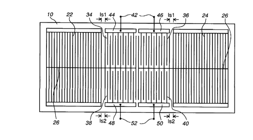
Referring now to Fig. 2, there is illustrated a double mode SAW resonator in
accordance with an embodiment of the invention. The resonator includes the reflector
gratings 22 and 24 on the substrate 10 generally as described above, except that in this
case the reflector gratings 22 and 24 need not be grounded. The IDT 12 of Fig. 1 is
divided in Fig. 2 into two differential halves 34 and 36, and the IDT 14 of Fig. 1 is
divided in Fig. 2 into two differential halves 38 and 40.
As is clearly shown in Fig. 2, the electrodes of the IDT half 34 extend between the
inner rail 26 and an outer rail 44, and the electrodes of the IDT half 36 extend belweell the
inner rail 26 and an outer rail 46. The inner rail 26 is shown in Fig. 2 as being divided
centrally into two halves, but this need not be the case and instead this inner rail 26 could
be continuous throughout the length of the resonator. As is also shown in Fig. 2, the
electrodes of the IDT halves 34 and 36 have a constant pitch of ~2 within the two IDT
halves and between the two IDT halves in the center of the resonator, but there is a phase
inversion between the two halves. This is lepresenled in Fig. 2 in that the adjacent end
electrodes of the two IDT halves 34 and 36 both extend from the inner rail 26, so that the
IDT halves 34 and 36 are arranged for operation with dirr~len~ial signals. Accordingly,
differential, or balanced, signal connections 42 are provided to the rails 44 and 46.
Similarly, the electrodes of the IDT half 38 extend between the inner rail 26 and an
outer rail 48, and the electrodes of the IDT half 40 extend beLweell the inner rail 26 and an
outer rail 50. The electrodes of the IDT halves 38 and 40 have a constant pitch of ~J2
within and between the two IDT halves, and there is a phase inversion between the two
IDT halves 38 and 40 represented in Fig. 2 in the same manner as described above. The
IDT halves 38 and 40 are thus arranged for operation with differential signals, and
differential, or balanced, signal connections 52 are provided to the rails 48 and 50.
As shown in Fig. 2, the fingers of the reflector gratings 22 and 24 are spaced from
the electrodes of the IDT halves 34 and 36 by separations lsl, and the fingers of the
~135983
~,
s
reflector gratings 22 and 24 are spaced from the electrodes of the IDT halves 38 and 40 by
separations ls2. The separations lsl and ls2 are shown the same in Fig. 2 because this is
a schem~tic diagram, but preferably they are dirr~ t in order to cancel or reduce the level
of spurious and higher mode SAWs in the resonator. These separations are discussed
further below with reference to Figs. 3 and 4.
It should be appreciated that the reflector gratings 22 and 24 produce between
them a gap or cavity within which SAWs det~rmin~d by the IDT electrodes resonate,
thereby creating a standing wave pattern. Figures 3 and 4 represent the standing wave
pattern, referenced 54, and the positions of the electrodes of the IDT halves and the
fingers of the reflection gratings in relation to this pattern. Fig. 3 illustrates electrodes of
the IDT half 34, showing in conventional manner by + and - signs their relative polarities,
and ~ cent fingers of the reflection grating 22, also illustrating the spacing lsl. The
arrangement of the electrodes of the IDT half 36 relative to the fingers of the reflection
grating 24 is symm~trical to this. Similarly, Fig. 4 illustrates electrodes of the IDT half 38
and ~ sent fingers of the reflection grating 22, also illu~ g the spacing ls2, and a
symrnetrical arrangement applies to the electrodes of the IDT half 40 in relation to the
fingers of the reflection grating 24.
Referring to Fig. 3, the electrodes of the IDT half 34 are centered over the
st~nlling wave maxima of the SAW potential. The fingers of the reflection grating 22 are
offset from this, being positioned with an edge of each finger over the m~illlulll of the
st~n-ling wave; the illustration in Fig. 3 assumes that the SAW reflection coefficient is
positive at this edge to produce constructive rather than destructive reflections.
Consequently the separation lsl is equal to 0.625~. Fig. 4 is similar except that the
separation ls2 is increased by ~2 to 1.125~. In general, each of the separations lsl and
ls2 has the form 0.625~+n~/2, where n is zero or a positive integer.
Fig. 5 illustrates an equivalent circuit of the SAW resonator of Fig. 2. In thisequivalent circuit resistors Rl and R2, inductors Ll and L2, and capacitors Cl and C2
have m:~gnit~ldes given by the equations Rl=Ra/4, R2=Rs/4, Ll=La/4, L2=Ls/4,
Cl=4Ca, and C2=4Cs, where Rs, Ls, and Cs represent the resistive, inductive, andcapacitive motional (i.e. not static) colllponents of a symmetrical vibration mode
resonance frequency Fs of the resonator, and Ra, La, and Ca represent corresponding
components of an anti-symmetrical vibration mode resonance frequency Fa, with coupling
represented by four transformers T each with a 1: 1 turns ratio and a winding sense as
represented by dots in Fig. 5. Capacitors Ct represent static capacitances of the IDTs; for
simplicity other static capacitances, for example be~weell the balanced signal lines 42 and
52 at the input and output respectively, are not shown in Fig. 5.
The SAW resonator described above can for example be used as an IF
(intermediate frequency) bandpass filter in a broad-band radio receiver, its balanced input
2135983
42 being coupled via a ~ g circuit to the b~l~nce~l output of a buffer stage, and its
b~l~nced output 52 being coupled via a m:~tching circuit to the balanced input of a low-
noise amplifier stage. Each m~trlling circuit can comprise a b~l~n~e~l alrangement of
series capacitances and a shunt inductance, or series inductances and a shunt capacitance,
5 and serves to properly ~ the SAW resonator and to compensate for the static
capacitances Ct. In such an arrangement, Fs and Fa correspond to the lower and upper
edges of the passband of the filter. Higher order spurious modes can be attenuated by
more than 30 dB relative to the pa~sb~ncl, and the matched insertion loss of the SAW
resonator itself can be about 1.5 dB.
The positions of the electrodes and fingers shown in Figs. 3 and 4 relative to the
standing wave pattern 54 provides the strongest electromechanical coupling to the
resonant cavity, but long IDTs are necessary to obtain strong coupling (i.e. low loss) on
weak coupling substrates like quartz. This has the undesired effect of increasing the
cavity length, which reduces the longitll-lin~l spurious mode spacings and thus allows
spurious modes to appear in the reflection grating stopbands. This effect is avoided by an
~1 le- - -~l ;ve embodiment of the invention represented in Fig. 6, which provides inherent
suppression of spurious longit-~lin~l cavity modes.
Referring to Fig. 6, the electrodes of the IDT halves 34 and 36, and the electrodes
of the IDT halves 38 and 40, are displaced from the center of the SAW resonator and are
positioned in spatial synchronism with the fingers of the reflection gratings 22 and 24.
Thus there is a constant ~2 pitch of the fingers and electrodes between and within the
reflection grating 22 and the IDT halves 34 and 38, and between and within the reflection
grating 24 and the IDT halves 36 and 40, so that the IDT electrodes con~tit~te part of the
grating arrays. The resonant cavity is then reduced to a length ls between the IDT halves,
which are dirrcrenlially excited as described above via the balanccd signal lines 42 and 52.
The shorter cavity length also makes the resonator less sensitive to fabrication variations
than the arrangement of Figs. 2 to 4.
The arrangement of Fig. 6 provides a balanced SAW resonator in which a
co~ roll~ise is made, depending on the separation ls, between the m~ximllm st~nlling
wave and suppression of spurious modes. For example, a value of ls-0.4375~+n~2,
where n is zero or a positive integer, provided a desirable performance with only a slight
increase in matched insertion loss of the SAW resonator itself to about 2 dB. As in the
resonator of Fig. 2, in the SAW resonator of Fig. 6 the value of ls between the IDT halves
38 and 40 can be dirre~ t from that between the IDT halves 34 and 36.
The arrangements of Figs. 2 and 6 can be combined, for example as shown in
Fig. 7. In the SAW resonator illustrated in Fig. 7, the IDT halves 34 and 36 are arranged
as described above with reference to Fig. 6, and the IDT halves 38 and 40 are a~ranged as
described above with reference to Figs. 2 and 4.
2135983
In each of Figs. 2, 6, and 7 the inner rail 26 is shown as being divided into two
halves, but as already stated this need not be the case, and the inner rail 26 can be
continuous over the entire length of the SAW resonator. In the latter case, the SAW
resonator can also provide a balanced-to-nnb~l~nced coupling, for example as described
5 below with reference to Figs. 8 to 11.
In the SAW resonator of Fig. 8, coupling is provided between the two IDT halves
34 and 36, arranged with b~l~nced signal lines 42 as described above with reference to
Fig. 2 and 3, and the IDT 14 arranged with an unbalanced signal connection 20 asdescribed above with reference to Fig. 1.
In the SAW resonator of Fig. 9, coupling is provided between the two IDT halves
34 and 36, arranged with balanced signal lines 42 as described above with reference to
Fig. 6, and the IDT halves 3B and 40. In this case the IDT halves 38 and 40 are arranged
in a similar manner to that shown in Fig. 6, but are both coupled to the same outer rail 19
to provide an unbalanced signal connection 20 as in the resonator of Fig. 1. Accordingly,
in the resonator of Fig. 9 there is no phase inversion between the electrodes of the two
IDT halves 38 and 40. Thus in Fig. 9 the electrode of the IDT half 38 which is closest to
the resonant cavity, or the center of the resonator, is shown as extending from the inner
rail 26, whereas the adjacent electrode of the IDT half 40 is shown as extending from the
outer rail 19.
In the SAW resonator of Fig. 10, coupling is provided between the two IDT
halves 34 and 36, arranged with b~l~n~ed signal lines 42 as described above withreference to Fig. 6, and the IDT 14 arranged with an unb~l~nced signal connection 20 as
described above with reference to Fig. 1.
In the SAW resonator of Fig. 11, coupling is provided be~ween the two IDT
halves 34 and 36, arranged with b~ nced signal lines 42 as described above with
reference to Fig. 2 and 3, and the IDT halves 38 and 40, arranged in the same manner as
described above with reference to Fig. 9 to provide an unbalanced signal connection 20.
The advantages of the short resonant cavity provided in a SAW resonator as
described above with reference to Fig. 6 can also be provided in a SAW resonator having
llnb&~ nced input and output signal connections. Such a SAW resonator may be
particularly useful in circuits, such as oscillator circuits, which do not require balanced
connections. Examples of such SAW resonators are illustrated in Figs. 12 and 13.In the SAW resonator of Fig. 12, coupling is provided between the two IDT
halves 34 and 36 and the IDT 14 which is as described above with reference to Fig. 1.
The two IDT halves 34 and 36 are arranged with a common outer rail 16, unbalanced
signal connection 18, central resonant cavity belween the two IDT halves, and no phase
inversion of the electrodes adjacent to this cavity, as described above for the IDT halves
38 and 40 in the resonator of Fig. 9.
~135983
In the SAW resonator of Fig. 13, coupling is provided between the two IDT
halves 34 and 36, arranged as described above with reference to Fig. 12, and the two IDT
halves 38 and 40, arranged as described above with reference to Fig. 9.
Although particular embodiments of the invention have been described in detail, it
S should be appreciated that numerous mo~1ific~tions, variations, and adaptations may be
made without departing from the scope of the invention as defined in the claims.For example, although IDT halves 38 and 40 are referred to above and illustratedin Figs. 9, 11, and 13, and IDT halves 34 and 36 are referred to above and illustrated in
Figs. 12 and 13, the electrodes of the IDTs providing an unbal~nrefl signal connection
10 could more generally be divided into two groups of unequal si~, with the resonant cavity
between the two groups.
In addition, although the invention has been described in relation to double mode
SAW resonators, it is equally applicable to other surface wave resonators which may use
surface skimming bulk waves rather than surface acoustic waves. Two or more SAW
15 resonators may be connected in tandem, as is known in the art, in order to provide desired
response characteristics, such resonators being provided either on separate substrates or
on a single substrate with a desired separation be~ween them. As already indicated, the
fingers of the reflection gratings 22 and 24 can have a pitch dirr~c"l from that of the IDT
electrodes, and as is known in the art the reflection gratings could be con~tit~lted by
20 grooves in the substrate instead of fingers on the substrate, or could be dispensed with
entirely if the IDTs are sufficiently long to provide adequate coupling between them. In
addition, dirr~ t sizes of the resonant cavities may be provided, and other parameters of
the resonators may similarly be changed to suit particular re4uhclllcllls.
Furthermore, although as described above the resonators of Figs. 2, 6, and 7 are25 described as providing b~l~nced or dirrtlcnlial input and output connections, it should be
appreciated that, provided that the inner rail 26 is not grounded, the same resonators can
be used to provide unbalanced input andlor output connections, simply by connecting one
of the dirrclcll~ial connections to an llnhal~nced signal termin:~l and the other of the
dirr~ ial connections to ground. The same applies to the dirr~ "Lial connections in the
30 resonators of Figs. 8 to 11. Thus, in particular, a single four-termin~l resonator as shown
in Fig. 2, 6. or 7 can be used to provide a balanced-to-balanced, balanced-to-unbalanced7
or unbalanced-to-unbalanced coupling between its input and output.