Note: Descriptions are shown in the official language in which they were submitted.
CA 02135995 1999-02-O1
TFT WITH REDUCED PARASITIC CAPACITANCE
FIELD OF THE INVENTION
This invention relates to a TFT (thin film
transistor) array in an active matrix liquid crystal
display (AMLCD) having a plurality of TFTs arranged in
the form of a matrix, each TFT including a gate
electrode, a semiconductor film, a drain electrode, a
source electrode, and a pixel electrode stacked on a
transparent insulation substrate.
BACKGROUND OF THE INVENTION
Active matrix liquid crystal display devices are
composed of a matrix of liquid crystal pixels arranged
horizontally in rows and vertically in columns. The
individual liquid crystal picture elements or pixels
include first and second opposing polarizers, a liquid
crystal material disposed between the polarizers, and
transparent electrodes mounted on opposite sides of the
liquid crystal material. Individual pixels of active
matrix liquid crystal displays are more fully described
in U.S. Patent Nos. 4,632,514; 5,150,235; and 5,161,041.
Electronic matrix arrays find considerable
application in active matrix liquid crystal displays.
Such active matrix displays generally include X and Y
1
~~.~~)~~~~
address lines which are vertically and horizontally
spaced apart arid cross at an angle~to one another thereby
forming a plurality of crossover points. Associated with
each crossover point is an element to be selectively
addressed. These elements can be, for example, liquid
crystal display pixels or the memory cells of an
electronically addressable memory array.
Some form of isolation device (e. g. a thin film
transistor] is generally associated with each array
element or pixel. The isolation elements permit the
individual elements or pixels to be selectively addressed
by the application of suitable read potentials between
respective pairs of the X and Y address lines.
Amorphous semiconductor thin film field effect
transistors or TFTs have found wide usage for the
isolation devices in such arrays. Thin film transistors
formed from deposited semiconductors such as amorphous
silicon alloys are ideally suited for such applications
because they exhibit a very high dark resistivity and,
therefore, have very low OFF state currents. The reverse
leakage currents are so low that very high ON-to-OFF
current ratios are made possible for effectively
isolating the non-addressed array pixels from the pixels
being addressed.
.~ Structurally, thin film transistors (TFTs) generally
include substantially co-planar source and drain
electrodes, a semiconductor material between the source
~I~~~~-~~..~~
and drain electrodes, and a gate electrode in proximity
to the semiconductor but electrically insulated therefrom
by a gate insulator. Current flow through the thin film
transistor between the source and drain is contrblled by
the application of a voltage to the gate electrode. The
voltage to the gate electrode produces an electric field
which accumulates a charged region near the
semiconductor-gate insulator interface. This charged
region forms a current conducting channel in the
semiconductor througku which the device current is
conducted.
Figures 1 and 2 show a conventional linear-type thin
film transistor used in conjunction with an active matrix
liquid crystal display. Referring to Figures 1 and 2, a
plurality (not shown) of TFTs 1 are arranged on a
transparent insulating substrate 2 in the form of a
matrix. Gate electrodes 3 of the thin film transistors 1
are connected by a gate line 4 extending in the row
direction. Drain electrodes 5 of the thin film
transistors 1 are connected by a drain line 6 extending
in the column direction. A source electrode 7 of each ,.
thin film transistor 1 is connected to a transparent
1 , ,'pixel electrode 8 independently formed in an' area'
surrounded by the gate,and drain lines 4 and 6. The .
pixel electrode 8 is the transparent electrode adjacent a
Image
~1~~~~~
The linear type thin film transistor of Figures 1
and 2, unfortunately, has a relatively high parasitic
capacitance which tends to cause pixel flickering, image
retention, and gray scale nonuniformity. The relatively
high parasitic capacitance (C~s) of the linear-type TFT
shown in Figures 1 and 2 causes the pixel voltage across
the liquid. crystal material to drop by about 1-2 volts
when the voltage signal to the gate electrode is shut
off. The pixel voltage drop or shift is determined by
the following equation:
svP - cgs . sv9
. . ' C9S 'f' CST + C
where CST is the storage capacitance, which is added in
parallel to the liquid crystal capacitance C~~. The
parameter 8V9 is the gate pulse height. 8VP can be offset
by adjusting the voltage on the counterelectrode (on the
top plate) to get a substantially pure AC voltage across
the liquid crystal material. However, because C~~ depends
upon the voltage across the,liquid crystal material, bV
can generally not be offset for every gray level and, for
large displays, cannot be offset over the entire display
area. The residual DC component can lead to pixel
I flickering,-image retention, gray scale nonuniformity and
electrochemical degradation of the liquid crystal
material.
As the parasitic capacitance of a TFT is decreased,
the voltage drop and corresponding DC component across
5
'
-the liquid crystal pixel becomes smaller. Accordingly,
the voltage drop across the pixel is proportional to the
parasitic capacitance or CAS of the TFT. The relatively
high voltage drop across 'the ;prior art pixel discussed
above leads to flickering, image retention, and gray
scale nonuniformity in the pixel display. Flickering r
results from a small DC component across the pixel
electrodes spanning the liquid crystal layer.
Accordingly, pure AC voltage across the pixel electrodes
is ideal. By reducixig the CAS, or parasitic capacitance
between the gate and source electrodes of a TFT, the DC
component across the pixel electrodes of the prior art
TFT of Figures 1 and 2 can be substantially eliminated or
reduced, thereby greatly reducing pixel flickering, gray
scale nonuniformity, image retention, and electrochemical
degradation of the LC material.
Therefore, there exists a need in the art for a thin
film transistor (TFT) having a reduced parasitic
capacitance CAS for use in active matrix liquid crystal
displays.
Figures 3 and 4 illustrate an attempt, described in
U.S. Patent Nos. 5,003,356 and 5,055,899, to reduce the
parasitic or gate-source capacitance CAS present between
the gate and source electrodes. The prior art open-ring
thin film transistor of Figures 3 and 4 includes a gate
electrode 1.L formed on a glass substrate 12, and a gate
insulating film 13 consisting of silicon nitride and
rY; . ....: ~ . .:: ., '..: ' .; ~ ., ; . .t.., -.. . S :~ .?~ " : , :
....,..; ,. - . . , " ., . ~ :, j1 '::, .N, ,,., ' .:, ,
. , . .,..
., '~ .:.~. .':'~, '., ~.~,.. :. '.. '.: ,. ,.~::.. ... '. ....:. .",'.
,'.. ... :,:.'~,':... :. ..'..,''.
.,,./.:., '..;.'_., .: ':~,.'. ~..".'/.. m: ,. ,..:'' ,' , .
:' ,.:... .......v ...' .., ...:..~.. ; -....,.,.... ... . .
:'.:.. '~....,
t
'
. . , . ' : ;.
.'' ..:.W, '...'; /':~ ,../!.:: ~ ..,.. :
..:,: .., :"-..::'., : :.' ;.:.' '' .::::... '.. .~', , . . r~' ~.. '
'.,...'
i " ' .,.. ~~...:'.
J .,. ,.."...:.. . . ,:!..,v ,.:,.,:_. ....'. ~. . .;. .... .. ..
,..:'...
.~..:,h'n:.:...; ..:' ,: . :.':.' .' : :.::~ . n.':. , ' :% -. :.:.. .., .,.
.:..~.".. .-....,
r,
.... . . ."..' ...,
".. ~...~ ./..
. ''." . '"..,...... ";..
..... . ,.
.:. :."".. ,...:.....:. ...v'...:.. .. .::::.,,. ":' : .:'...:.,
'
,,.,. /:... ,
,..... ...:.".,
.:..._...;.. .
..:.': .. .
:: '.'.... .
,..,'.;,,,.r-.::.
'-. n..:'..._:. .,.,.::...:.'. .., ,.....';....w.:~: :'.''.:
:..,':'~.:
:':'. "::::.. : .,.'.::,~ '.'.v':'.: ~..,. . .....~..w,: ..
...,. ..:
.; ;"., /, . .~ .:..; ..n..' ... ..,......, .._ '......,r.,..:: '; a:....
.. , . .:~.:. ....,..... :'....W;.../,/.,~:..: ...:..,.. .'.:.'J..
.., ._... -. ....
':.... m...,...' r .':..:. :. .. ..:::.:..,.'..:. ...:..- .'
:.: ~.!..'".....'~~-'~' ...,..,. .. ..._,..::. . ::,:.' ::....: .:!'..::.
,:~..
. .:-" .~... ..,.: ~.....
'... ' f... . .1
.!.
:i..'.
.. , .: . ., :: . :" . .; ;':r> . ':: . .... :', ~' .;:.~:,.,
.: z'. ,r " ;: ;;. .. :;'; .,. ..,.. ..
t
. A.~ 1.,,. i;,..F' ...
.;:.,. .,y;,. . '. ,:::. ':_,',, . ....
.! ...
.,.,'.'.:..:,..t. ,J'~,-:. ':.'. t.:.':. ~:.
.~ :: :''. a..i.. .. . '"..: " -. "
s'!.
:
J
'
. ,
' ,
' .: ..": '
.':..'.' '
.... '..,'....:,...
,. , .../. . .,.~ '. ', .;.: ..:. :
:. ,' .. .. ,'''..'!. ' , :' . ,. ~,: ".'. ' ~. ' : . ' ', / '
. .' . .;...r.. -:.1, .,.,..~..' ...:.'. .. , . ... .
.. . '._. ,.. ':....,. ',. . ...':.n . - '... .........n,.:.....,..
;.: .'..' : " ::!. ~ '.:., f..f ri .,:..:.;' '.:, .S: '.:.'"' .'
.:~:': ' .'.' ..
f. '
t , t. :.i.l. /. t:'
.
....
: t. ~
: .;..
,..
. "::
.'.: :'.
'..
'
:
,
~
'
:
s
/
'
. .
. :
t,..'.. , ,~,
....: r . ..,
'... n ..' ~,I ':
.. '
t...,.......,.,.'_..,"!
... ."..;. .
,..- '.
... " . .... .
. .
.
...~::.. ;.:
'
::'." . .
;::. .... !.
..~.'... ;.t....~': ..,., .. :.'. '.. :.! . ,'.'.: : , r.".;
! .. . , ."."~.' :.''" ~ . ." ., . :..,..., ..'...::.... ',;..
.,.'.. n, f: , n...: .. :'.. ~,. .
.. : '...:. ...,. ; ' ..... .::'...: r.,.-.'.:; ..".~-.,r.....;.
.".'.. .,. ...':'.: r, .'/...!./:1......:.'...- 1.
.v./ '. . /....
... ... ' , " .:...": /.'... /~ ; , n .".. . .:... . , '' . ..
'.:' .:~'..;._:. . '~.~.',:.,. .. ~,.:. , .. . ': '. ' ....:.,
,. ...
'
L
'
'
W f'
-
.
::
'
/
'
..
'..'. .:. . . .
. . .. :..., ,
. .
( ./ ,:
;: . . ..', . ' .
.; .: ~. '. .: . . .... .. . :. .. . ., ....
, . ~:.''..::'...:.. . .
' . .
,
..
.. . . :.
/,t
,..,,,..",,. . ':..,.,.. .. : ..". / ": '...' . ..,: ~' .,...
,'., . .._ ..., "..: .:.' ...' . / ... ..,;'...... ' r:.
r ... : , , . ..
- ~ . ..~ . ,
.. :,.r.. . .: .:~
~..'...,, ....' .': .'..-'~:. ' t";:/. .r.
.::..: .~:.. :.. :;:' '::.
,. .,...:. ..-:
'
'
, ,
:.~;.'~.....u.:.
,.:., , .. .
...:., .
'. ,, . ,. .
.....' .. .;.., :~.'.~' ::.I .... .. ::.-.l'.y.:,, r. . . ..:. .'.: '.
J.. :...1.. "::.r, .,: .". ,... .' :.... ....." , .... .,. .
,~: n;':, ;.'..: ; . '~'.'.!. , ,: .;. :. ..:,. , . ;./ ~:.: ,...:'.. ~
.:. ';..( ;..,.,.,.,. ',',: ,., . . ., .: '...: ! .. . , ::~w.:
'': .,,.. , ',. ., . ;.
- ''..:: ~.'. :;.:: : '; '': . w'. : . .~..:. ... /. . ;;,,..,
r. ' ::. , ...,.,.. , ,.. :.f_.v.y ":r.. .., :,, . .;.:. :.
' . . : .., ~ . .. ,
. . ...:. . ,'..n., , ''.. .:, '.' ;::,~ . ,:''~ . ' ''. '..
...~~. ' . ; . : .:', .. .:. . ~:,. .:'.::.. .:.,:'.~,:. '-'.:
, .
having a thickness of about 3,000 ~ stacked on the gate
electrode 11. A semiconductor film 14 consisting of
amorphous silicon (a-Si) is stacked on the part of the
gate insulating film 13 which corresponds to the--.gate
electrode 11. The a-Si layer 14 extends laterally at
least to the lateral peripheral edges of the gate
electrode 11. A partially circular source electrode 15
is formed on the semiconductor film 14. The source
electrode 15 has a diameter of about 4 wm (micrometers).
A drain electrode 16 is formed in a semi-annular or
half-circular shape on the semiconductor film 14 only
partially surrounding the source electrode 15, thereby
forming a semiconductor channel portion °'L" in.a
partially annular space between the source and drain
electrodes 15 and 16. Because the channel portion is
formed so as to partially surround the source electrode
15, if the distance between the source and drain
electrodes is a channel length L, and the length of an
arc defined by substantially intermediate points of the
channel length L is a channel width W, the channel width
W is sufficiently larger than the channel length L. The
channel length to width ratio is therefore less than one
thereby providing far a reduced parasitic capacit,ance,;C~s.
The source electrode 15 is only-partially surrounded by
the drain electrode 16 because the source and drain
electrodes are substantially coplanar and an opening is
left in the drain 16 to allow the pixel electrode .19, 25 ,., .,
7
~1~~~9~ ,
to extend into electrical contact with the source
electrode 15. Furthermore, the open-ring design of the
prior art TFT shown in Figures 3-4 is provided so as to
not unduly limit the viewing display area of the"arrayed
c~~r
circular shaped drain electrode 16, Therefore, the pixel
electrode (19, 25) does not cross over the drain
electrode 16 but, instead, extends through the opening
created in the drain 16. That is, the drain electrode 16
adjacent the linear portion 25 of the pixel electrode is
removed so as to prevent an t;tnnecessary electric field
from being applied to the channel portion.
In the prior art open-ring TFT of Figures 3 and 4,
the source electrode 15 is formed so as to be smaller in
size than the drain electrode 16. Therefore, the area
where the source and gate electrodes 15 and 11 overlap
one another is considerably smaller than that where the
drain and gate electrodes 16 and 11 overlap one another.
Accordingly, the parasitic capacitance, or CAS, between
the gate and source electrodes is decreased.
While the open-ring geometric design of the prior
art thin film transistor of Figures 3 and 4 does, in
faot, reduce the parasitic capacitance between the gate
and source electrodes, the open-ring thin film transistor
of Figures 3-4 is not without its drawbacks. The prior
art open-ring TFT is very photosensitive and the
parasitic capacitance CAS of the open-ring TFT shown in
FiguresV3-4 has not been decreased as much as would be'
most preferably desired. Furthermore, the linear
electrode portion 25 and the amorphous silicon '
semiconductor layer of this TFT are not completely
shielded by the gate electrode from the backlighting
9
scheme (not shown) by the gate, thus subjecting the thin
film transistor of- Figures 3-4 to undesirable
photosensitivity with respect: to the backlighting scheme
(not shown) of the liquid crystal display whichw
illuminates the pixels and TFTs from beneath the gate 11,
In fact, Figure 3 illustrates the edges of the
semiconductor layer 14 extending beyond the edges of the
gate electrode 11. Also, the ON current, an important
parameter in determining how fast the pixel will charge
up during the positive charging cycle, of this prior art
open-ring transistor is undesirably low. Finally, the
open-ring TFT shown in Figures 3 and 4 is located on the
gate line 2l, thereby reducing the display area of pixel
electrode 19.
The aforesaid described prior art TFTs are very
photosensitive. The reason for this high degree of
photosensitivity is that the semiconductor a-Si layers 1''"'' I
are photosensitive and axe not completely shielded by the
prior art gate electrodes from the intense radiation of
backlighting schemes because the prior art a-Si layers
extend at least to the periphery of the gate electrodes. ~~r','v-'v ''
It should be apparent to those skilled in the art
that there exists a need in the art for a thin film
transistor, in an .active matrix liquid crystal display,
having a reduced parasitic capacitance, a reduced
photosensitivity, a high ON current, and positonable so
as to enlarge the display areas of the pixel electrodes.
It is a purpose of this invention to fulfill the
above-described~needs, as well as other needs apparent to
the skilled artisan from the following detailed
description of this invention. w
S~JN~ARY OF THE INVENTION
Generally speaking, this invention fulfills the
above-described needs in the art by providing a pixel for
use i.n a liquid crystal display, comprising: a layer of
liquid crystal material sandwiched between two spaced
substrates, each substrate having a pixel electrode
mounted thereon, and wherein one of the pixel electrodes
is electrically connected to a thin film transistor, the
thin film transistor comprising: . ~,
a drain electrode adapted to be electrically
connected to a drain line; a gate electrode adapted to be
electrically connected to a gate line; and a source
electrode substantially coplanar with at least a portion
of said drain electrode and electrically connected to the
one pixel electrode; wherein the source electrode is
located on a semiconductor film and is substantially
completely surrounded in substantially all lateral
directions by the drain electrode.
In certain preferred embodiments of this invention,
'the. thin film transistor further comprises a passivation
,,
~1~~9~~
electrode electrically connected to the source electrode
is transparent and is adhered to and crosses over the
passivation layer.
In certain further preferred embodiments of this
invention the thin film transistor further comprises a
gate insulating layer disposed between the semiconductor
film and the gate electrode, wherein the gate insulating
layer includes a silicon nitride layer about 2,000
thick and a Tao layer about 1,600 ~ thick.
~ In still further preferred embodiments of this
invention, the gate electrode, not including the gate
line, has a larger horizontal surface area than the
semiconductor layer.
This invention further fulfills the above-described
,,~:
needs in the art by providing in an active matrix liquid
crystal display (AMLCD) comprising a plurality of thin ,v
film transistors arranged on an insulating substrate in
the form of a matrix, one of the plurality of thin film
transistors including a drain electrode electrically
connected to a drain line, a gate electrode electrically
connected to a gate line, and a source electrode
electrically connected to a transparent pixel electrode
of a corresponding pixel display, wherein 'the source and
drain electrodes of said one thin film transistor are
~I~~~9
wherein the source electrode of the one thin film
transistor is centrally located on the semiconductor film
and is substantially completely surrounded laterally by
the drain electrode. ._
In certain preferred embodiments of this invention,
the drain electrode is substantially annular or circular
defining an inner and an outer diameter, the source
electrode is substantially round, and wherein the gate
electrode is substantially round and has a diameter y
substantially larger than the inner diameter of the drain
electrode thereby increasing the tolerance for
misalignment of the source and drain electrodes relative
to the gate electrode.
In further preferred embodiments of this invention,
the gate line is arranged in a row direction, the drain
line is arranged in a column direction substantially
perpendicular to the gate line, and wherein the gate and
drain lines intersect one another defining the pixel
display area therebetween. In still further preferred
, embodiments of this invention, the thin film transistor
is located at an intersection of the gate and drain lines
thereby enlarging the size of the pixel display area.
display is adhered to and crosses over the passivation
layer, and wherein the pixel electrode consists
essentially of Indium-Tin-Oxide (ITO) and the passivation
' layer consists essentially of one of: silicon nitride,
silicon oxide, and combinations thereof. In certain
other preferred embodiments of this invention, the
channel is ringed shaped and ',has a channel length of
about 6 micrometers and the diameter of the source being
about 8 micrometers. '
In certain other, preferred embodiments of this
invention, the semiconductor film consists essentially of
amorphous silicon and is about 2,000 ~ thick.
This invention will now be described with reference
to certain embodiments thereof as illustrated in the
following drawings.
IN THE DRAWINGS
Figure 1 is a top view of the construction of a
prior art active matrix liquid crystal display utilizing
a conventional linear type thin film transistor having a
relatively high parasitic capacitance and high
photosensitivity;
Figure 2 is a cross-sectional view illustrating the
linear thin film transistor of Figure 1 taken along line
rx-II in'Figure 1; illustrating the layering system of
the prior art linear type thin film transistor;
14
~~3~~9~ .
Figure 3 is a top view showing the structure of an
open-ring prior art thin film transistor which utilizes a
round source and d semi-annular drain electrode only
partially surrounding the source electrode;
Figure 4 is a cross-sectional view showing the open-
ring thin film transistor shown in Figure 3, taken along
the line IV-IV in Figure 3, illustrating the layering
system of the prior art thin film transistor;
Figure 5 is a cross-sectional view of a first
embodiment of the thin film transistor according to the
instant invention, illustrating, the centrally located
source electrode and the annular or circular drain
...\
~~.3~99~
Figure 9 is a top plan view of a third embodiment of
the thin film transistor of this invention;
Figure 10 is a top cross>-sectional view of the
source and drain electrodes of the first embodiment of
the thin film transistor of this invention illustrated in
Figure 5;
Figure 11 is an equivalent circuit diagram of a thin
film transistor of this invention; and
Figure 12 is a cross sectional view of a liquid
crystal display pixel to be selectively controlled by a
TFT of this invention.
DETAILED DESCRIPTION OF
CERTAIN EMBODIMENTS OF THIS INVENTION
Particular embodiments of thin film transistors
(TFTs) according to this invention will now be described
with reference to the accompanying drawings.
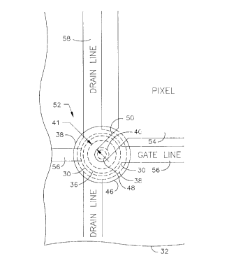
Figure 5 is a cross-sectional side view illustrating
a first embodiment of the ring-shaped thin film
transistor of this invention. Gate electrode 30
consisting of either chromium (Cr), aluminum (A1),
tantalum (Ta), or combinations thereof, and having a
thickness of about 1,000-5,000 ~ (most preferably about
;
2,500 ~) is formed on an insulating substrate 32
preferably consisting essentially of a transparent glass
plate. A gate insulating film 34 having a thickness of
about 3,000-4,000 ~ (most preferably about 3,600 ~) is
formed on the upper surface of the insulating glass
substrate..32 including the upper surface of the gate
electrode 30. The gate insulating film 34 ~.s made of,
for example, silicon nitride, silicon oxide, tantalum
oxide, or combinations thereof. This gate insulating
film 34 may include two layers (not shown), one of, for
example, silicon nitride, and the other of tantalum
oxide. If made of two layers, each gate insulating film
layer. most preferably has a thickness of about 1,500--
~Z~~~~~
38, are separated from each other by a predetermined
distance that forms a channel length portion 41.
In order to electrically connect the drain and
source electrodes 38 and 40 to the amorphous silicon
semiconductor film 36, the drain and source electrodes 38
and 40 are provided with contact films 42 and 44
respectively. Each contact film 42 and 44 preferably
consists essentially of one layer preferably made of
amorphous silicon doped with an impurity (e. g.
phosphorous) in a high concentration and having a
thickness of about 500 ~. Each electrode 38 and 40 is
preferably made of a conductive metal material such as
chromium. The drain and source electrodes themselves may
be about 1,000-5,000 ~i thick but most preferably are
about 4,000 .~ thick. As a result of the reduced surface
area of the semiconductor layer 36, a portion of the
drain electrode 38 is substantially coplanar with the
source electrode 40, while another portion of the drain
is not.
A passivation and insulating layer 46 made of ' w
silicon nitride, silicon oxide, or any other suitable
material is preferably deposited on substantially the
i ..
entire exposed surface above the insulating subst~ate'32
on which the above-described films have been stacked in a
predetermined form. The passivation layer 46 preferably
extends over the matrix array including the pixel, and
the gate and drain lines, and has openings only for the
18
~1.~~~~9~
thru-holes 48. Alternatively, the passivation layer may
have an opening for the pixels 54. The substantially
annular drain electrode 38 is preferably completely
covered with the. passivation :insulating film 46 and is
21~j~9~
transparent pixel electrode 50 extends into the thru-
hole 48 and hence is electrically connected to the source
electrode 40 thereby conductively connecting the source
electrode 40 to the pixel. A portion 51 of the '
transparent pixel electrode 50 crosses over the channel
portion 41 of the semiconductor film 36 formed between
the drain and source electrodes 38 and 40. The portion
51 of the transparent pixel electrode crossing over the
channel 41 forms a top gate transistor more fully
described below and schematically illustrated in Figure
11. Due to the presence of the passivation layer 46, the
portion of the pixel electrode 50 disposed above the gate
electrode 30 is generally not coplanar with either the
source or drain electrodes.
If the thickness of the passivation and insulating
film 46 formed on the drain and source electrodes 38 and
40 is excessively small, the passivation and insulating
properties of the TFT are degraded. In contrast to this,
if the thickness of the film 46 is excessively large,
electrical connection between the source electrode 40 and
the pixel electrode 50 through thru-hole 48 becomes
rather difficult. Accordingly, the thickness of the
passivation layer 46 preferably falls within the range~of
about 2,000-8,000 ~. Furthermore, as the thickness of
the passivation layer 46 becomes larger, the significance
and effect of the top gate transistor formed by crossover
portion 51 is reduced.
2~~~~~~
In the thin film transistor of Figure 5 having the
above°described structure, because the passivation
insulator layer 46 is formed on the drain electrode 38
and part of the source electrode 40, the pixel electrode
50 is provided with a bridge over the drain electrode and
~~.'~~~9~
a thickness of about 3,000°4,000 ~ and cover the gate
electrode 30. A silicon nitride film, silicon oxide
film, tantalum oxide film or combinations thereof may be
used as the gate insulating film 34.
Subsequently, the semiconductor film 36 made of
amorphous silicon or the like and the contact films 42
and 44 made of amorphous silicon doped with an impurity '
at high concentration (e.g. about 1~ phosphorous) are
continuously formed or stacked by plasma chemical vapor
ZO deposition or the like onto the gate insulating film 34
sows to have thicknesses of, for example, about 2,000 A
and about 500 ~ respectively. The semiconductor film 36
and the contact films 42 and 44 are patterned by
photolithography or the like so as to cover a portion
above the gate electrode 30. Instead of the above
mentioned amorphous silicon, amorphous silicon carbide
(SiC), tellurium, selenium, gerumanium, cadmium sulfide
(CdS), cadmium selenide (CdSe); or the like may be used
as a material for semiconductor film 36 and contact films
42 and 44.
A relatively thick metal film having a thickness of
about 1,000-5,000 ~ (most preferably about 4,000 1~) is
then formed on the entire surface extant by vapor'
deposition, sputtering, or the like, thus covering the
contact films 42 and 44. This metal film is then
patterned by photolithography, etching, or the like to
remove the film and contact films 42 and 44 at the
22
~~e~~~
channel portion 41, thereby forming the drain and source
electrodes 33 and 40 above the gate electrode 30, which
are separated from each other by a predetermined channel
length distance 41, as shown in Figure 5. Chrozziium,
~1~~~~J
Finally, the transparent pixel electrode 50 made of
a material such as ITO, tin oxide, or Indium oxide is
then sputtered and patterned on the top surface of the
passivation film 4f including the thru-hole 48 to a
thickness of about 1,000 Vii. With the above-described
process, fabrication of the thin film transistor of this
embodiment of this invention is completed.
Accordingly, the parasitic capacitance CAS of the
thin film transistor of this embodiment is improved due
to the geometric design of the TFT wherein the drain
electrode substantially laterally surrounds the source
electrode. By reducing the CAS, small DC components
across the pixel (between the opposing pixel electrodes)
are reduced thereby substantially reducing flicker, image
retention, and gray scale nonuniformity in the pixel.
As shown in Figures 6 and 7, a plurality of thin
film transistors 52 of the first, second, or third
embodiments of this invention are arranged on the
transparent insulating substrate 32 in the form of a
matrix, and are used as switching devices for
corresponding liquid crystal display pixels 54 wherein '
each pixel display 54 includes a liquid crystal layer,
opposing polarizers and a pair of opposing electrodes .
(one of which is the pixel electrode.50). More
specifically, a plurality of TFTs 52 are arrayed on the
transparent substrate in the column and row directions.
Cate electrodes 30 of the respective thin film
24
~1~~~~5
transistors are commonly electrically connected to
conductive gate lines 56 in the row direction. Drain
electrodes 38 of the respective TFTs 52 are commonly
electrically connected to conductive drain lines~~58 in
the column direction. Source electrodes 40 of TFTs 52
are connected to the transparent pixel electrodes 50,
which extend from their respective pixel displays 54 to
the thru-holes 48 thereby being electrically connected to
both the source electrodes 40 and pixel displays 54.
to Pixel displays 54 ar~.respectively arranged in a
plurality of regions surrounded by the gate and drain
lines 56 and 58, and are electrically independent from
one another. The edges of the pixels 54 are preferably
located closely adjacent the gate and drain lines, and
may even slightly overlap them.
Referring still to Figures 6 and 7, an opposite '
transparent substrate 60 (preferably on the viewer side
of the AMLCD) having a corresponding transparent pixel
electrode 62 formed on its entire surface is placed on
the substrate 32 on which thin film transistors 52 are
arranged in the form of a matrix in the above-described
manner so as to oppose them. A liquid crystal display
.
I : . ; .; ;
device is obtained by sealing liquid crystal material 64
between the opposing substrates 60 and 32. In this
liquid crystal display device, each transparent pixel
electrode 50 corresponds to one image displaying pixel or
.
25 ;.,,. . . ,..
>- :. .:. v;: -'y, . _:, ; .:. :. . - : .., .: ; :. ' ..' :,:.:
-: , , r" . . ,.::
:
:
;;.' , : .:~ ::.; :::..: . .. ,
:,: . . ,;r..,,, , :.I: ,, .. .~: : v..w...:.:,.,. r
, .. . .v.., v.:..:.'.. .':.,. ;v.:. . ' :.<.; ,
u.:, ,.: .,. . :: . . .;... . ;:": . , ,. , . . . - . ....: .: , . ::,
, .;. . l.. ;~.:, . .. , . ,.. .,.. . . .. .: .
,; ,.": .,..:.. : . ; .... .; . . ~:>., ,. ;. .:,. .. ,.. .. .'.:: , ,
: ,.,, ::: ., :.... -. . L.,.:; . ..:: ,... . ,
. :
'
'
. ' ": .:: .
. ,.. . ., ::: ::~ ..,: ;.:; L .::
; ,,. . .- ar..
... ...... ,:: . .w; ".. :. .. : .: .: , . . . :.
. .:' .. ,, " .r. . r... . ,.,.". ..... .~ .::". , :,..,. . .., :, ,...:.:,
:..... .. ,,., , .. .. ,:..,.. . ~,.;,1, .;; ,.. .. ... ,.
. . .
.
,~,
.
.
:
:
~:.
."
.
1
,
" ,. . .
:. ,
;.,:, .. ,: . :, :: : . "
. . . :, ..
. . ;..; , ,: . :.
. ..
.,.: ,..;. ,
,.... .,;., . , -:: . . . :. ..... . ,.
,.. :: ., ~;,.. .
. : . . .;::r:.. :.. : . .r
.. .
.. , r
, .;
, . . .., .. . ., , ..,.. ,. ..:. , . .. ,~;.. ,.... ., :., ., ,.
-,: - , ... :.:., .-, .., .1:.. 1 . ::. :.; .l. .','. . .: .:,. .,,
:' . . ,.,.
~,... . ,.~.., z ,
;,.;:. ,;, : ,.,.,. ~.,:.. ./.;:.:,.:.., '::.. '~ .:.. .'. .'..'.':.;
:, .,:,...;, ... , .,..,:'.. .....
;~.." ... : 1... ,. .'. _ ,,... , ,. : .: . .... : ..,. . . ..
, ,. ..,. ... .. .,:.: : ,.,.. . . .., . .
...,
.
,.
.
,.
...
.
:.
..
,,.:,,
,
.,
."
I . .
:
_
,
:
.
:
:
~
~..
.'
. i-..
,: "
. ;
. ;
.. , :
. .
.: . . ..
.. ;:, . .
... ".;. ;,
:- .
:'. .. ., ,
, .
I .
:'.., . .:~::.:,
.... : a'.: ,
: "
..
.
.
.
. : ..
: , :,,
.:
.
.
.
,.. . . .. .. ,..,, . . .. , ,. . ,. , ...." . -. . . .:. , .
~ .. ,' . . . , . ...
.,.. ,:', : ".. ,,. .;, .,,, ,.'.:,.. .. ,.:, , ,.., . ; ',.,;:
,: , .-, " . ~ ,;:, ..:.. :.., .I.:.: ' ..
. ,:: . : :. -. :,:. . .. . . .., :: .... . ...,..,. : :. . .
. . ;...;..... .;. : . . . . . ; ,.. : .:. , .. ., .. ,
. l.~ -I -.t '. I I
:.~,_ ......... . . .:. ," ...,:: . .:" !:',.. .
.'.:.; . ,. :..~.: ~::: ;y.: ' ''
::.'r~'.. -- r ;:.:.',' :.
.I ...~~ :
'
' ~
,. ...
, . ..
."
.:..:.".-.: ..
!.:...... .
. ::.....~":...
....:. !) '.
..., :. ...~..,'.'.:.~ ,' :; .....':..., ,.'::...,. ~:..,. ,sir .r:~.
..'.:;;r:G
... ,.: I....;. ~,.. .:::: :':. <.: -.".-;: '.,:. .,'. ..
,' , a.... :.: ,.;.: ,;"...:... ..:.::' ..~....,:....:..~.:..n
:.........r..:.,.,.,1.'..:'.
, , :.':~. v:::::'.:~.1...:~:.':.~. ... ... .....~:. .:' ...,..,
'!,'..: ~:,. . ,..... '. .,:..., l , ,;..: "-: .1.;..:: .., :.,':.:~,.;..'
' ...., .. ,
' :..;: ..::'~.,........ ,...;.: ~ , :.. ;, '..~~.nj. ;,:.. ..:;.':
.... , '.::y -;~:..; ,.::......... ,: ...,.......:. ..:-.'
, ':
.
.
:
'
'
:' ' , . .r,
. : ,r',. .,
. . :..., .
:..,n .. .,n...'
I. .: ~,,. .;.'r .' ... .
,., ,..: .::'.'
::. . ,,. :::.,. .:' :. .....,;. ,... ,:. '~.,:,. ,. ',:' . : .':,, '.....
.,. :....:.."'....:: .. ...:, . , . :.,: . 1 .::: .,. .' . ~:..
. . '......, . :: v . ::.. ~ , :.. ..'..':. ,.: 1...!,,. ,,;s..'
... : : .~ :..,::', r: :.:.'..' . :'.'.......: ..: .,.;'.' ..~ ... ,
.- . .. _ .
.: .. , ... ~ , . . ..r ' ,r ' ., :.,.. ~.,: I" '...:. .. ~_.u: .."..
. :. . :.::: .':-:. :.. :..:s ..... ., '.,..I:. .. ....:._.,.;.
; ..:.:. : r ... ,._.,.. . ,..., .:. .. .,,. , :..:: ~. .
) . .,. . , .:... :.,, , . . : ' .
I: ..... , ; ....~'v. . .,.,.
: ; ... .:
.
':
'
::
, .
, , .
.
, ..
. ,.,.,.. , :;,... .:! ;
L ......':: .,..f, ,.,, ,..,..
.... ~.:, .:: , !n/ !... , ....:.,:...:
,:,..., ".....: ..: .:.. .'::.'.~ :' :._:.., .;...: .:.,~.:. . ..
": . '.. .... ~ .. ;..: ...._. ., ., .: ~ : ,:.:..: :.~ ..~. ..... .
~,.'~..:
I' '.. .... . .1.,.~ .. . .. '.. '. :.':.'. ...:.. .. . .i.__,.... ... .
: .'. .. .. . ..':
....:...v,......':.... ~... ..,..::., .,.., ::,. '.i, . ., :. .,..'',
'...:..:.',-',..~.../.
.:'... ,..,..,;~::.n: ,:,:,:': ..'. ..,. ~;. ~.' :r. ".:.n
.:...~;...'~.:'....'~.
.. ... . ..:.. ' .
'. / . , .... . .,.,. . .. ,.. ...... .. . . . . .. ... t ~. ... ... ..
~ . .. . . .. .. . ....,.Y.. , .,n r . . . ..
2~.'~ ~~~~
picture element of the active matrix liquid crystal
display.
The above-describea active matrix liquid crystal
display device is operated in the following manner. Scan
signals are sequentially supplied to the plurality of
gate lines 56. Data signals for controlling the ON/OFF
states of the respective pixels 54 are supplied to the
plurality of drain lines 58 in accordance with the timing
of the scan signals. Thin film transistor 52 whose gate
electrode 30 has received a scanned signal is turned ON,
reads a data signal supplied at that timing, and
thereafter supplies the data signal via a voltage~to the
pixel electrode 50 and a resulting electric field is
applied to the liquid crystal material 64 located between
the pixel electrode 50 which has received the data signal
arid the transparent electrode 62 of the opposite
substrate 60 in accordance with a potential difference
between the opposite electrodes.' Then, the orientation
state of the molecules of the liquid crystal material 64
is changed, and thus transmission and interception of
light are controlled according to the polarizers (not
shown) .
As'described above, in the liquid crystal display~of
this embodiment having pixel electrodes formed on thin
film transistors, the passivation insulating film 46 of a
particular TFT is formed on at least a drain electrode 38 .
of the TFT, and the transparent pixel electrode 50 is
26
~~.~r~~95 ,
formed on the resultant structure. Therefore, short
circuiting between the transparent pixel electrode 50 and
the drain electrode 38 can be prevented. In addition,
due to the location of the thin film transistor of this
embodiment at the intersection of the drain and gate
lines of the matrix array, the distance between the pixel
display and the drain and gate limes, i.e. distance A in
Figure 1, can be set close to 0 in the practice of this
invention, thereby enlarging the pixel display area.
Accordingly, a maximL.m effective pixel display area is
obtained. In this embodiment, a pixel display opening
ratio of about 53.5 or more can be realized as opposed
to that of about 50~ in conventional linear TFT devices,
such as that shown in Figure 1.
Because the step of forming the transparent pixel
electrode 50 is the last one, and the source electrodes
of all the arrayed TFTs are commonly connected upon
deposition of the transparent conductive film before the
step of separating the transparent electrodes 50
individually is executed, operations of all the TFTs can
be measured within a short period of time by bringing the
probe of a measuring device into contact wzth a plurality
I of gate and drain lines and the transparent conductive
film while supplying test signals.
~ Figures~8 and 9 illustrate second and third
embodiments of the ring-TFT of this invention. Figure 8
is a top view illustrating an octagonal source electrode ~''~'
:.: .- -.. 'v : , : ,:.~ .. ,.._ .: ,, ;, ., ,,, . . ,. ,.; ., ., :, ~ .'
w ' . ; , . . .
.-. .y ...- ~ ;.,.,; ..,., -.,.,:. .;~ ..,' : . . .:: ;.'.: : -. .;: '- .
;.-: ,; " ,
. .-=- : . :.~: , . , :.~. : :' .. ; ;" , ~; : , r"; y ., ~,
- -: .. , ., ~:: , :-, ;;; :;y :: .., ,,
.. .',' , - .;- 'c: ':.. . ,,; y :, ,,.,. , ,,._ : , ,... ;, , .:'.
,. : , .: ,.... ,
,:. -..: ~ . - "; - , '-
,\
~~.3~~9~
40 completely surrounded by a substantially annular
octagonal drain electrode 38. The diameter of the source
electrode 40 shown in Figure 8 is about 10 micrometers
before etching and about 8 micrometers after etching of
the electrode material. The channel length 41 of the TFT
shown in Figure 8, as in all of the TFTs illustrated in
Figures 5-11 herein, is about 4 micrometers before
etching and about 6 micrometers after etching. The
channel width W (see Figure lo) as in all the TFTs
illustrated in Figures 5-11 herein, may be determined via
conventional mathematical formulations.
Figure 9 illustrates a thin film transistor similar
to the second embodiment illustrated in Figure 8
described above, except that the source electrode 40 has
an island diameter of about 8 micrometers before etching
and about 6 micrometers after etching. As can be seen in
Figure 9, the width of the pixel electrade 50 is
substantially similar to the diameter of source electrode ".
40 in contrast to the embodiment of Figure 8 where the
width of the pixel electrode 50 is slightly less than the
diameter of source electrode 40. Alternatively, the TFTs
of Figures 8 and 9, instead of being octagonal, could be
elliptical, hexogonal, circular, or rectangular. The ~' ',
reference numeral 90 is the photoresist pattern used to
pattern the a-Si semiconductor layer, and 36 is the '
resulting a-Si layer.
28
'' , . , , . .., .. : . '. , . ; ;
.. .' .. ' ;: , :; .: :,.:: ' ;' , ~ ~ ~ . , . ;~ ; , , . ~ ; ., . ~ ,
. , .,: ~ , : . ' , . .. -.
.,,,. , '.;. " , ; . , : . ',';: ;; ;:',, ::: . ~>,,. ;:,,
- : , ". ~ '. '' . ;' . ; .
.\
21~~~~~~
The resulting semiconductor layer 36 in Figures 8-9
has an outer lateral edge about 0.5-2.0 ~.m inward from
the outer lateral edge of the gate electrode.
Figure l0 is a top cross-sectional view illustrating
the cross-sections of the source electrode 40 and drain
electrode,38 of the first embodiment of this invention
illustrated in Figures 5-7. As can be seen in Figure 10,
the annular or circular drain electrode 38 completely
surrounds centrally located round source electrode 40.
Because the channel portion 41 between the source and
drain electrodes is formed so as to completely surround
the centrally located source electrode 40, the channel
width W is sufficiently larger than the channel length L.
Therefore, the L/W ratio of the channel length L to the
channel width W is substantially less than one. Because
of the geometric design of the TFT of this embodiment o.f .
this invention, the gate source parasitic capacitance Cps '...v
can be made small compared to the capacitance generated
between one pixel electrode 50 and the opposing pixel
electrode.62 through the liquid crystal material 64.
,'.: ,.,:;: y,.
Therefore, the influences of gate signals on source
potentials can be reduced thereby reducing flickering of
the pi~cel. Because the channel width W can be increased,
high drive performance of this.TFT can also be realized. ,
By reducing the parasitic capacitance, the small DC '
components across the pixel can be substantially
eliminated and flickering, image retention, and gray
2~.~~~!~
scale nonuniformity can be greatly reduced, if not
eliminated.
The parasitic capacitance Cps of the ring type TFT of
the first embodiment of this invention is defined by the
following equation:
2 _D2
Ccs <max3 - 7C Dl In ( D1 ) C°x
As can be seen from this equation, variables D1 and
D2 (see Figure 10), D1 being the radius of the central
round source electrode 40 and D2 being the inner radius
l0 of the drain electrode 38, determine the parasitic
capacitance of the thin film transistors of this
invention. By varying D1 and D2 (changing the size of
the drain and/or~source electrodes) one may fine tune the
parasitic capacitance of a given TFT to.-~ desired value.
The parameter C°x simply represents the gate insulative
capacitance per unit area.
The thin film transistors of the above-described
embodiments of this invention also have a substantially
reduced photosensitivity. Backlighting assemblies (not
shown) of active matrix liquid crystal displays are
~; , ~.
positioned below substrate 32 and emit intense radiation
onto the pixel including the TFT. Because of the design
of the TFTs of the above-described embodiments of this
invention, wherein the transparent pixel electrode 50
2:I~~~95
50 is shielded by the source, gate and drain electrodes
from the heat and radiation generated by the backlighting
assembly. Furthermore, the amorphous silicon layer 36 is
photosensitive and needs to be shielded from the
backlight by the gate electrode. In these embodiments,
the a-Si semiconductor layer 36 does not extend to the
lateral periphery of the gate electrode 30 and is
therefore not exposed to the backlight radiation as in
the aforesaid discussed prior art TFTs. Accordingly, the
' TFT of these embodiments are less photosensitive.
Therefore, the TFTs of this invention also have the
advantage, relative to the open ringed TFT shown in
Figures 3-4, of having a reduced photosensitivity due to
the geometric design of the semiconductor layer, the gate
electrode, and the crossover aspect of the pixel ,,
electrode crossing over the drain electrode. The gate w
electrode 30 has a larger horizantal surface area than
the semiconductor layer and therefore effectively shields
the photosensitive semiconductor layer from the backlight
radiation.
~~.3~~9~
embodiments of this invention have an increased margin
for misalignment in the manufacturing process. The prior
art TFTs shown herein in Figures 1-4 have no such
tolerance for misalignment. w
The above mentioned tap gate thin film transistor
formed by the crossover 51 of the pixel electrode 50 over
the annular channel 41 will be discussed as follows.
Where the portion 51 of pixel electrode 50 crosses the
channel 41, a small top gate transistor is formed with
the passivation insu~.ator layer 46 acting as the gate
dielectric. The equivalent circuit for this
configuration is shown in Figure 11. Only when VSp (the
voltage between the source and drain discussed in the
examples below) is positive and larger than the threshold
voltage of this top gate transistor, is an accumulation
layer formed at the interface of the.passivation layer 46
and the semiconductor layer 36, and an excess leakage
current is observed. This parasitic top gate TFT has a
substantially higher threshold than the main ring TFT
formed by source 40, drain 38, semiconductor 36,,and gate
30. During normal operations of TFTs in an active matrix
voltage and normal positive voltage (e. g. about l0 volts)
on the source electrode. However, for larger positive
voltages on the source electrode (e. g. about 20 volts)
increased OFF current is observed. Because, during
S wormal operations of typical active matrix liquid crystal
displays, the positive voltage on the source is
maintained at about 10 volts, the parasitic top gate .
transistor formed by the crossover 51 of the pixel
electrode 50 over the channel 41 is not detrimental to
the operation of the 'TFT of the above-described
embodiments of this invention.
It should be clear that the TFTs of the above
described embodiments may be further optimized as needed
by increasing the threshold voltage (Vih) of the parasitic
top gate TFT by, for examgle, proper choice of
passivation layer material, interface treatments, and
increasing the thickness of the passivation layer.
A possible modification to the thin film transistor
of the above-described embodiments of this invention will
be described as follows. A contact metal (not shown)
consisting essentially of a conductive metal material may
be buried in the through hole 48 formed.above the source
' ,
electrode 40, and the transparent pixel electrode 50 may
then be deposited on the resultant structure, thereby
electrically connecting the source electrode 40 to the
:w~
the like and is formed in the through hole 48 by
electrolysis plating. In this modification, the source
and pixel electrodes 40 and 50 are connected to one
another through the contact metal (not shown). Hence,
electrical connection therebetween may be ensured. This
modification allows simpler electrical connection of the
pixel and source electrodes and is especially useful when
the thickness of the passivation layer 46 is increased
above about 400-500 ~.
A second possible modification of the ring-shaped
TFT of the above-described embodiments of this invention
is as follows. The above-described illustrated
embodiments of this invention show the passivation
. insulator layer 46 having a substantially constant
thickness across each of the source electrode 40, the
semiconductive layer 36, and the drain electrode 38.
Alternatively, the passivation layer 46 may be deposited .
on the above-described films so as to define an upper
surface thereof being substantially flat. This would
allow the pixel electrode 50 to be deposited onto a flat
upper surface of the passivation layer 46, thereby
allowing the transparent pixel electrode to be more
easily and'simply deposited onto the passivation layer'.'
Figure 12 illustrates a pixel display 54 of this
invention to which thewpixel electrode 50 is electrically
connected. The pixel electrode 50 extends between the
pixel 54 and the source electrode 40 of a TFT of this
34
r4 .. -...: ..:: ::: .'. .....::. ,. .'.' , ; : : . ' .:~. , '.:;'. ..,.:
-'i., ~... :.:::;' .., ~:::'~ :"...., ,:,.;.., ::~:::. .: :::".
:, , .... ,. , .,. . . . ; .. . -I .,..: .., , . . . . , . ,
... .. ' ;. . :,." .. t .:.:':;.. ... l . '.;i,
:. ' ..: . ~. ,.'~. .. ~ , ...,.. .: . '..: ... . . .. ' .....,.: :
:.. .... :.,r . ,, ,. . ,. .,, .
.. " ...
:.~:.v ,,:'.
~
'"
,.;":: ,, ~:.:
', ,.,v.: . 'v;:':
'
.;
:, ':;'
:;~~~''
. ,~'
.,...
':..-' '':::
, ::'~'
~
.:~.
;...,.. ;.,,.,.
;, . ~:,.:: ,
b ...,. . .
:. .. . ,
. ,.. ... ,
.: .. ,
.... . ...,.r
.,. . :...:.;..
. .
t... , .'...:,,
~.~. . ,::...
: .
' ..
' ,
.
~.,..;.. .::.' , y::.:,' '.;..:;:.' -.':.: 1 :'.:':. . ..'..;:.
:.'.;.'. . . ': :'~.': ..;~:.:. :;.'.,'':.: ' :..;:. .,...;;.;:'.
...,..;... .. , ;.;.: , : .,. , -.,. : ... .. r. .'......~ .
,:~. .:~..: .... .. _..... ,.. , ....1:,-.' . ,...., ; ..., :,,.
.::.~. .:.-,..:. . .....
.:. . , . .... . . ..;... . ........:: . .:...:....,. .:. ...:.
: '..'.,. ......,. ..... .... . ;,':.., ......: 7 r.,..:~ ,.'
'..... . ',. ...: . .. ..::,
, ..:.: ,~~:~."-' .,..-...., ....::,.. ;;., :::'::' .~:: ,::,.'...,:
.::: :::._.~.. .:"'. ~.. ....'I ;...:.. .:,... . ;..'.:"..~.;
...
.
::,.
.y
.,
.; "'
:
..~r.
'
':.
:;.''
,
;:
y
:,
'
'.
,'
:
.. , ,
i ,,
,: ,
,
,.
;.' "'
.
a
,
,
, ..
..
..:
:
.
..
.
:
:
.
!, a .
.:_
!;!;',
'
:v
!..
1 .
1 t r
r
n i ~ nw~.....
1
s
,1
. 1 a
1~....,.
,1 ..: I
!L !..
.:f . . !.'..,.
t 1
> .y
i
..l'.. ~
II'...
-:
,..
V ~''
1 .
5 :
I
.
'
1
1
~:
.
. , '', n .
.
......'. :.I
' .
...'. .
. .
1
- J
., !,. ''
.'.
nl:.
.:1:, ,
'...
.
'~'
'.
~: "'.
.....
,
.
'
'
:
~
-
'
'
'
~
~
.
. ,
. ,
: . .
. ,. ..
, .
.:. '.. , , .
t..'., .. ,.
: ,.....:...( l'
...,
r ..
. : .~.
I.
' ..:'
...
..
.
..'.~,
..:....' l ~ :. : .. ,....... . . .. :,.1.. .. .:..'.. . .....
, .: , .:.::..,; :..:: ~.r-.t ~..
.. : , .. ':..., : .. . '..~. :. :.':.:n.
,lil.',
1.
1
y.'-
,. 1
-
/ .
1 rr:.
f ..r
:.; i:
iifrlr .,
;
.Y... ,.
;::
4.
, .
,
. ..! \
.1
::. S '
1 ..,.. :. ,r'.'
t. .
,tJ , r-
rr. .
: !..:~.:'. .,,;, ;.
!
:.,'.;;.
,: i::
,
::: .l..:
' .a.. r; :'.,!
' .:
: '.
i;:~
.,"; :~
.. ,s:
-:'
:~
'
'
. ,.
'~,
,
'
~'
'
:
v
~ 'v
'
. ..
. '
..: ,
. .
,.:.:: ,. .
.;.,:, ,., . .. '.
w, . ~' ....
, :
., ,
.
;
, .
.
'
: ! "
. . . :::
'
,
:
.
_ ; . ,....". . ~;.: .:., . . ,... ,';:'. ', , ::. , :..,, ,':,,.
. . ;:' -. ~; ~ ;': ' .'.;% , ,:'':- ' :'. ,. .. _:.... .:
~~.3~~9
invention. An opposing pixel electrode 62 is disposed on
the opposite side of the liquid crystal layer 64 and is
mounted on the lower substrate 60. Polarizers 71 and 72
are on opposite sides of the pixel and may be crossed or '
paral3el thereby creating either a normally white or
normally black display. Orientation films ?4 and 75
align the LC material 64 adjacent the films 74 and 75 in
predetermined directions (preferably at angles
perpendicular to one another) thereby preferably creating
l0 . a twisted nematic liquid crystal cell. The color filter
may be, for example, red, green, or blue. The pixel 54
shown in Figure 12 is merely one pixel or subpixel in the
array of LCD pixels 54 shown in Figure 6.
This invention will now be described with respect to
X13 i~9~ .
conventional linear type TFT similar to that illustrated
in Figures 1 and 2 with a layering system similar to
those of "Type A'° and °'Type Et°' .
EXAMPLE 1
The first.:'rFT formed according to this invention,
''Type A", was formed as follows. This TFT had a cross-
sectional. view similar to that illustrated in Figure 5,
having a lower insulating substrate upon which a gate
electrode, a dual layered gate insulating layer, a
semiconductor layer, a contact layer, source and drain
electrodes, a passivation insulator layer, and a
transparent pixel electrode were formed. The source -
electrode was round having a.diameter of 6 ~m and the
drain electrode was circular or annular and completely
surrounded and was partially substantially co-planar with
the source electrode. The lateral edges of the a-Si
semiconductor layer did not extend to the periphery of
the gate electrode. The channel length was 6
micrometers. The semiconductor layer was formed of
amorphous silicon and was 2,000 ~ thick. The gate
insulating layer was a dual layered system with a 1,600
,' , , , .
thick Ta0 layer and a 2,000 ~ thick silicon riitric~e
layer.. The,temperature was 26°C. The gate electrode was
about 2,500 .~. thick and the source and drain electrodes
were about 4,000 ~ thick. Table 1 below illustrates the
36
~~.3~~995
resultant ON and OFF currents as well as the parasitic
capacitance C~~ of this "Type A" ring-shaped TFT.
TABLE 1 --
'°Type A'° Ririg TFT
IoN (+) (~,A) 10.1
IoN (-) (~,A) 7.42
IoFF ('~) (PA) 0.5
IOFF (-) (PA) 0.09
CAS (min) (fF) 33
, CAS (max) (fF) 47
(~'a Was measured with VG = 20V, VS = IOV, and Vp =
OV.
The "+" refers to positive VSp, and the "-°' refers to
the probes being switched on the source and drain
electrodes.
ImFF was at VAS = -5V, VS = lOV, and Vp = OV.
(min) was the parasitic capacitance when the TFT
was OFF, and CAS (max) is the parasitic capacitance when
the TFT was ON. CAS was measured as a function of. VAS with
a Keithly 3330 LCZ meter. The meter had a resolution of
10 ~5F (1fF) .
EXAMPLE 2
A second ring-shaped thin film transistor ("Type B")
according to -this invention was formed as follows.
The "Type B" TFT of this example also had a cross--
section similar to that illustrated in Figure 5. The
channel length was 6 micrometers. The layering system
~~.~~~9~
and respective thicknesses thereof were similar to those
described above in Example 1, but the temperature was
27°C. The principal difference between the TFT of this
example and that of Example 1 was that the source'
electrode of this example was round and had a diameter of
8 micrometers. Therefore, while similar TFTs were made
in Examples 1 and 2, the principal difference is that the
central round source electrode of Example 2 had a
diameter about 2 micrometers larger than that of Example
l0 1. Both TFTs of Examples 1 and 2 had round centrally
located source electrodes and circular or annular drain
electrodes completely surrounding the source electrodes.
Table 2 below illustrates the current, voltage, and
parasitic capacitance characteristics of the "Type B" TFT
of Example 2.
.. ;:
TABLE 2 ~''.;-.:.::..:.:"
"Type B" ring-shaped TFT
- IoN (+) (~A) 13.9
IoN (-) (~A) 11.2
, IoFF (+) (pA) 1.15
IOFF ( ) (pA) 1.47
Ccs (mln) (fF) 40
Cps (max) (fF) 60
,, The above-listed parameters of Table 2 were
'.
determined using the voltages and probes listed in Table
1:
38
r
a
EXAMPLE 3
A partial ring-shaved TFT ("open-ring TFT") was
formed as follows. The "open-ring TFT" was formed in a y
manner identical to the ''Type B" TFT of Example 2 except
that the drain electrode was horseshoe shaped with the
source-drain metal removed under the crossover bridge 51 w
illustrated in Figure 5. Although this "open-ring TFT"
did not have a drain which completely or substantially
surrounded the source, its drain electrode surrounded the
source to an extent greater than that shown in Figures 3-
4 herein. The temperature was 27°C. Table 3 below
illustrates the current voltage, and parasitic
capacitance characteristics of the "open-ring TFT" of
Example 3.
TABLE 3
"Open-Ring TFT"
(+) (~A) to.7
U -) (wA) 9.4
IOFF (~) (pA) 1.6
2~ CcsF (xn n)(p ~F) 45. 18
CAS (max) (fF) _ 76
The above-listed parameters of Table 3 were
determined using the voltages and probes listed in Table
1.
39
2~.3~~~~
EXAMPLE 4 -
A "linear TFT°' similar tc that shown in Figures 1-2
was made and tested as follows. This linear TfT had a
cross-section including a lower insulating substrate upon
which a gate electrode, a dua~ layered gate insulating
layer, a semiconductor layer, a contact layer, source and .
drain electrodes, a passivation insulator layer, and a
transparent pixel electrode were formed. The channel
length was 6 wm and the channel width was 36 Vim. The
l0 semiconductor layer was of a-Si and was 2,000 ~ thick.
The temperature was 29°C. The gate insulating layer
included a 1,600 ~. thick TaO layer and a 2,000 .t~ thick
SiN layer. Table 4 below illustrates the resultant ON
and OFF currents as well as the parasitic capacitance CGs
of this ''linear TFT."
TABLE 4
''linear TFT"
IoN (+) (p~A) 12.4
ToN ( + (~A 10.09
OFF ( ) (p )
IoFF (.°) (pA) 0.09
Cos (min) (fF) 65
Cps (max) (fF) 115
The above-listed parameters of Table,4 were
i
determined using the voltages and probes listed in Table
Table 5 below compares the current and parasitic
capacitance of the four TFTs of Examples 1-4.
,'\
TABhE 5
'°comparitive results"
"open -"linear
'°Type A'° °'Type B" rind TFT" TFT"
Io (+)
~Et,A ) 10 .1 13 . 9 10 . 7 12 . 4
I (-)
o~~,A) 7 . 4 2 11. 2 9 . 4 12 . 3
Io F. (~)
~pA) 0.5 1.15 1.6 0.09
Io F (-) ,
~pA) 0.09 1.47 0.18 0.09
Ccs (min)
( fF) 33 40 45 65
Cps (max)
(fF) 47 60 76 115
As shown in Table 5 above, the TFTs of particular
embodiments of this invention ("Type A" and "Type B")
have parasitic capacitance CAS significantly.lower than
those of the "linear TFT'° and the "open-ring TFT". The .
"Type A" TFT has the lowest Cps, but its ON current is
reduced relative to that of °'Type B". Therefore, "Type
B" has the best performance with about a 22~ reduction in
CAS (max) relative to the "open ring" and almost a 500
25, reduction in Cps (max) relative to the "linear TFT'°, while
,. , , , , ,
sacrificing only about 10~ in ON current IoN (-) relative
to the °'linear TFT" and having about a-15-20% increase in
ON current relative to the "open ring TFT". The ON
current Ion (-) is the ever important parameter used in
- 41 '
X23 ~~~~ ,
determining how ,fast the pixel will charge up during the
positive charging cycle. CAS (max), the gate source
capacitance in the TFT ON state, determines the pixel