Note: Descriptions are shown in the official language in which they were submitted.
IPEAlUS 4NOV 1993
213 610 9 1 Re~lacement Paq~
--- PATENT
Attorney Docket No. 1813A-42g
ARTIFICIAL DIELECTRIC CONSTANT
MATERIAL AN~ M~T~Q~
~ACKGROUND OF THE INVENTION
A dielectric material is a material which, when in
the presence of elec~ric field, store~ more energy than is
~tored in free ~pace. That is, the dielec~ric material tores
electrical potential energy inside it~elf. Many common
material3, ~uch as glasq and epoxies, act as dielectrics,
This ability of the diel~ctric i9 commonly exprP3sed
in terms of permittivity. The permittivity for free space i9
identified as ~O while relative permittivity for a material,
unitless, i9 identified as ~r and i~ equal to the ratio of
permittivity of the material to the penmittivity of free space.
The rela~ive permittivity for air i9 approximately equal to 1.
For purposes of thi~ applicatio~, permi~tivity means relative
permittivity unles~ otherwi3e indicated.
In the presence of tlme varyi~g electric fields a
dielectric diqsipates a portion of it3 stored energy as heat.
Thig lo~g ia indicated by as3igning the penmittivity real and
imRgi~ary parts for the special case of steady state
sinusoidally varying field~.
Thu9 the complex penmittivity i3 defined by the
following equation:
~r = e~ , where j = J=~.
The~e real and imaginary parts are in general
functi¢ns of the frequency (~) 90 that the permitti~ity is
better expre~ed a~ the following:
~r ( ~ je// ~ ~ ), where j
5T~,'TE S~,~E~
W093/243~7 2 1 3 6 i 0 9 PCT/VS93/04069 ~
See Fig. 1 for a plot of ~(~) as a function of
frequency for a simple material. It is seen that as frequency
increases, ~ attains the value of 1, that is the permittivity
of free space, while ~ n has one or more peak valueq at special
~reque~cies. The imaginary part of the permittivity, ~", acts
like the first derivative of ~'. That is, where the rate of
change of ~' is the greatest, ~" peaks to provide what is
called an absorption band.
One of the uses for dielectric materials is in the
form of lenses to increase the amount of power that an antenna
can collect. Such lenses work because electromagnetic
radiation travels slower in the lens than in free space and
thus bends. A lens, to be effective, must have a diameter
greater than two times the wave length (~) of the
electromagnetic radiation. Since the wave length equals the
speed of light divided by the frequency, at a frequency of, for
example 200MHz, the wave length will be about 5 feet.
Therefore, extremely large lenses are required at radio
frequencies. This makes the use of natural dielectrics, such
a3 glass and epoxies, impractical for radio frequency lens
applications because of their weight. To overcome this
ob~tacle investigators in the late 1940's and 1950's
demonstrated that artificial dielectric materials could be
made.
One type, termed metallic delay media, can be made of
sheet~ of foam material with flat metal squares fixed to at
least one of the surfaces, the metal s~uares being separated
from one another. See S. B. Conn, "The Electric and Magnetic
Constants o~ Metallic Delay Media Con~aining Obstacles of
Arbitrary Shape and Thicknessn, J. of App. Phys. Vol. 22,
No. 5, May 1951 pp. 628-634, the disclo~ure of which is
incorporated by reference. The pieces of foam with the metal
squares are then stacked and secured together to obtain a
light-weight dielectric. The material can be shaped to create
3~ a lens to cause concentration of an electromagnetic wave passed
through the material.
. ,, " ,~ .
~ 93/24307 ~!~ 213 610 9 PCT/US93/U4069
., ~,.~,. , .
These materials behave in a manner similar to a
resistor capacitor inductor (RCL) circuit. Thus, by minimizing
the resistance of the obstacles a very low loss dielectric can
be made~ Near the frequency where the obstacles are one half
wave length long, the material behaves as a resonant ~C circuit
causing the permittivity to be strongly frequency dependent.
When this effect is undesirable, the obstacles are made very
small, effectively pushing the material resonance outside the
desired band of operation. On the other hand, if a designer
makes a prism having a dielectric constant which changes
rapidly with frequency (and thus with wavelength), a single
transmission can be separated in space into it~ individual
frequencies. That is, the signal can be multiplexed. In
communication this is quite useful since the more frequencies
available, the more information can be transmitted.
Because the early applications of artificial
dielectrics were for the purpose of enhancing the transmission
of energy, the greatest concern was in obtaining a controlled
real part of the permittivity ~'. The control of ~" came with
the need to absorb or attenuate electromagnetic waves.
In its simplest form such a material starts with a
host material into which a "lossy" material, like carbon, is
introduced and dispersed throughou~ the volume. This type of
dielectric material is termed an absorber.
The permitti~ity of this type of material is in
general frequency dependent and unpredictably 90. Even ~ery
fine particles of carbon tend to make tiny chains or groups of
carbon particles within the host material. The tiny chains are
separated by gaps creating a multitude of RC circuit analogs.
~ecause of this tendency, the final complex permittivity is
influenced by the amount of carbon present and is sensitive to
the process used in making the ma~erial. The carbon can align,
segregate or clump at random. These random effects reduce the
repeatability of these materials and frequently lead to
unplanned anisotropic properties. (Materials with anisotropic
properties exhibit different dielectric properties depending
upon the direction of the electric field.) Therefore, the
W093/Z4307 ' t2;i~-3 6 1 0 9 PCT/U593/0406 ~
making of an isotropic (essentially equal dielectric properties
in all directions) material u~ing microscopically sized carbon
particles by randomly scattering it throughout the volume is
undesirable from a manufacturing reliability standpoint.
A different approach to electromagnetic wave
absorption is embodied in circuit analog absorbers. Fig. 2
illustrates a single sheet of plastic having a number of cross
shaped elementq against which a wave i9 projected. The sheet
acts in the manner shown in Fig. 2A; that is, as an RCL series
circuit where the resistance is detenmined by the conductivity
of the elements, the capacitance is determined by the spacing
and size of the elements, and the inductance depends on the
size, width and shape of the elements.
In the embodiment of Fig. 2, part of the wave is
reflected, part passes through and part is dissipated within
the material. Using this principle, a circuit analog absorber
can be designed by stacking a precise number of sheets with
specific properties at precise spacings as show in Fig. 2B. In
this case the distance d between the sheets is equal to one
half the wave length. With this arrangement, the multiple
reflections between the wave and the various sheets are
precisely balanced with the impedance of each sheet to obtain
-~ absorption over a broad band of frequencies.
SUMM~RY OF THE INVENTION ~~
The present in~ention is directed to a method for
making a material-with an artificial dielectric constant. The
in~ention allows the material designer to construct
électromagnetic absorbers with tailor-made electromagnetic
properties. In addition to con~entionàl control of
conductiYity profile, control of the frequency dependent
permittivity of the material can be achieved independently
along all three principal axeQ of the material. The in~ention
thus has particular advantages for use with anechoic chambers,~ 35 compact range absorbers, absorbers used to eliminate
electromagnetic interference between neighboring
:~ .
~ O 93/24307 21~6109 P~r/US93/04069
telecommunication devices and absorbers for reducing the
deleterious effects of nearby structures on antennas.
The method is carried out by selecting the desired
dielectric constant, typically between about 1.03 and 20., for
a particular electromagnetic ~ield. A sub~tantially non-
electrically conductive sheet material, from which the material
is to be made, is choQen. An el~ctrically conducti~e material
is then applied to selected areas on the sheet material. After
such application, a cellular core material is formed from
10 layers of the sheet material ha~ing the conductive material ¦ -
already applied thereto.
Presently, loaded conducting foams or similar
materials, typically ha~ing finely divided carbon mixed
throughout the material, are used to attenuate unwanted
electromagnetic signals. However, the material properties are
not tuned to the frequencies of interest. Only the
conductivity profile and the material thickness are ~aried in
an attempt to meet the requirements. However, these two
variables are not enough to obtain a compact, higher
performance material for the application.
One of the primary advantages of the invention is
that it permits the designer much more latitude in the physical
construction of various absorbers. For example, conventional
low frequency (VHF-UFH) and anechoic chamber absorbers are made
with pyramids of absorbing foam as much as two meters tall~
With the present in~ention, using materials which are tuned to
the various frequency needs, the size of the resulting
absorbent structure can be significantly reduced.
In addition to control of the permittivity's
frequency dependence, its isotropy can also be controlled.
Therefore, the in~ention is ideally suited for use with spiral
antennas. Spiral antennas are often used in communication for
access to broadband frequencies for botn recei~ing and
transmltting purposes. Such antennas are also used for
nondestructi~e testing where they are used to emit and recei~e
broadband frequency pulses.
W093/24307 '~ 1 3 6 I O 9 PCT/US93/~06
Other ~eatures and advantages will appear from the
following description in which the preferred embodiments have
been set forth in detail in conjunction with the accom~anying
drawings.
S
BRIEF DESCRIPTION OF THE DRAWINGS
Fig. 1 plots the real and imaginary parts of
permittivi~y as a function of frequency for a typical lossy
dielectric;
Fig. 2 is a simplified view illustratins a single
sheet of plastic ha~ing a number of, for example, cross shaped
element~ against which a wa~e is projected so that some
radiation is transmitted, some is absorbed and some is
reflected;
Fig. 2~ shows how this sheet of Fig. 2 acts in a
circuit analog manner as an LRC series circuit;
Fig. 2B shows how a number of the sheets of Fig. 2
could be stacked at precise spacings equal to one-half the wave
length to achieve absorption over a broad band of frequencies;
Fig. 3 is a simplified schematic view suggesting one
method for manufacturing a honeycomb type core material made
according to the precent in~ention;
Fig. 3A illustrates the six differe~t combinations of
electric field polariza~ion and wa~e direction for the
artificial dielectric made of hexagonal cells according to the
invention;
Fig. 3~ illustrates a preferred hexago~al cell
geometry for use with the present invention;
Fig. 3C is an idealized view of the smallest periodic
unit of sheet in the core géometry shown in Fig. 3B;
Fig. 4 is an enlarged ~iew of the grld pattern of
Fig. 3;
Fig. 5 shows a second pattern of electric conductive
material according to a second embodiment of the invention;
Fig. 6 shows a third embodiment of the invention in
which electrically conducti~e material is applied to the sheets
in an undulating, generally M-shaped pattern; and
~ ~93/~4307 ~ 21~6109 PCT/US93J04069
Fig. 6A shows a set of six of the undulating
conductive elements of Fig. 6 arranged in array to illustrate
the cell lengths; and
Fig. 6B shows a hexagonal cell with the undulating
pattern of Fig. 6.
DESCRIPTION OF THE PREFERRED E~ODIMENI
The present in~ention is described with reference to
three different embodiments, all of which are made using sheets
of material which axe formed to create an expanded honeycomb
core type of cellular core material.
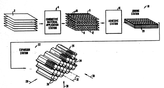
Fig. 3 schematically illustrates one way to make
honeycomb type cellular core material. Con~entional methods
for making honeycomb core material are described in more detail
in U.S. Patent Nos. 3,470,053 and 3,598,676, the disclosures of
which are incorporated by reference. Briefly, sheets of
material 2 are used to create the honeycomb type core materialO
Material 2 is preferably a resin-impregnated fabric type of
material, typically made of woven or felted fabric impregnated
with a phenolic resin. The fabric can be made of gla~s fibers,
quartz fibers, ceramic fibers, polymer fibers such as aramid,
or any other suitable material. Suitable fabric can be
purchased from DuPont Corp. of Wilmington, Delaware as Nomex~
brand aramid ibers. Other manufacturers of suitable fibers
include Clark Schuebel, Owens Corning, J.~. Stevens and Allied
Signal.'
Sheets 2 then pass through a conductive material
application station 4 which applies, in this first embodiment,
a grid pattern 6 (shown greatly enlarged in Fig. 3 for sake of
clarity) of an electrically conductive ma~erial ~. Material 8
typically includes finely divided carbon as the conductive
element suspended within a carrier fluid which e~aporates after
being applied to sheets 2. An example of a suitable material
is carbon loaded ~nks made by Olin Hunt Specialty Products Inc.
of West Patterson, N.J. Various other types or conductive inks
can be u9ed as well. The application of electrically
conducti~e material 8 to sheets 2 is preferably done by the
2136109
W093/24307 '~ t ~ ~ r PCT/US93/04069
rotogravure process, but can be accomplished by various other
con~er.tional processes including silk screening, ink jet
printing, lithographic printing and flexographic printing as is
shown in the art. Grid pattern 6, shown in more detail in Fig.
4, includes first and second sets 10, 12 of parallel, spaced
apart grid elem~nts 14.
Sheets 2, with electrically conductive material ~
applied thereto, then pass an adhesive station 16 at which a
suitable adhesive is applied to one or more opposed surfaces of
sheets 2. Sheets 2 are then placed one on top of the other at
a joining station 18. The joined stack 20 of sheets 2 then
pass an expansion station 22 to create an ex~anded honeycomb
type cellular core material 26 having electrical properties
created by electrically conducti~e material 8. Alternatively,
sheets 2 could be corrugated and then bonded together to create
the honeycom~ structure.
Grid elements 10 are oriented in the L (for length)
direction 28 while the elements 12 are oriented in the T (for
thickness) direction 30. T direction 30 lies parallel to the
axes 32 created along interiors 34 of the honeycom,b cells 36.
Directions L and T are perpendicular to one another. The W
(for width) direction 38 is oriented generally perpendicular to
the surfaces of sheets 2 and perpendicular to directions 28,
30.
Elements ~0 ha~e a width 40 while grid elements 12
have a width 42. E1ements 10, 12 define a unit cell length 44
in T direction 30 and a unit cell length 46 in the L direction
28. In the preferred embodiment widths 40, 42 are both about
0.02 inch to 0.10 inch while unit cell lengths 44, 46 range
from about 0.02 inchlto ! 0.30 inch.
The object with this embodiment is to use the control
afforded by line widths and line spacings to achieve a sheet
loss that is X for an electric field aligned with the T
direction 30 and, for example, 2X for an electric field aligned
with L direction 28. This can be accomplished in a number of
, . . .
:- ~ ways.
,, ~
:: :
~ ~?93/24307 2i36io8 PCI/US93/04069
Firstj let line widths 40, 42 and line conductivities
be equal. Make unit cell lengths 44, 46 be 0.1 inch and 0.2
inch, respectively, 90 that cell length 46 is twice cell length
44. This makes the resistance per unit cell twice as large for t
5 an electric field aligned with T direction 30 as for an
electric field aligned with ~ direction 28 to achieve a greater
conductivity in the ~ direction by a two to one margin.
A second way to achieve the two to one (or other)
conductivity ratio is to leave line widths 40, 42 the same and
10 unit cell lengths 44, 46 the same. However, line conductivity
in the L direction 28 can be made to be twice that in T
direction 30. This can be achieved in various ways. Two
~` different types of electrica}ly conductive material 8, one with
twice the conductivity as the other, can be applied. Another
15 way is to apply material 8 twice as deep or thick in L
direction 28 as in T direction 30 so that the electric field in
L direction 28 sees twice the conductivity, and thus twice the
108s, as in T direction 30.
A third way for achieving the two to one ratio of
ZO ~ sheet~loss~in the ~ and T directions is by leaving the unit
cell~lengths~ 44, 46 equal, the line depth or thicknesses the
same~but~ake the ~ direction line width 40 be twice the T
direction line width 42. Since line widths 42 of grid elements
12~w111~then be thinner than line width 40 of grid elements 10,
25~ an-~electric field oriented in T direction 30 will see the
thinner, and thus less lossy, line widths 42 than an electric -~
field direction in L direction 28 which sees thicker line
"; ~
wîdths 40. Also, a combination of these three methods can be
used as well.
` ! ~eing able to easily and simply adjust the loss
characteristics in this manner, the overall 109s
characteristics~for cellular core material 26 can be easily and
simply adjusted.
Cellular core material can be created from sheets of
material which are uniformly preloaded with a conductive
material. Such core materials generally exhibit anisotropic
behavior since they have different loss characteristics
.. . .
, ~ ~
W093/24307 2 ~ 6 1 0 9 PCT/US93/~069 ~
depending upon whether the electric field is in the L, T or W
- directions. In some situations isotropic (equal loss
charac~eristics in all three dimensions) behavior is desired.
~ The present invention is quite suitable for those situations as ~ ,;
well, since the sheet anisotropy can overcome certain
anisotropy due to cell geometry as is discussed below.
Fig. 3~ illustrates a preferred cell geometry for a
- hexagonal-shaped cellular core element 48 for use with all
three preferred embodiments of the present invention. This
cell geometry produces a 2:1 anisotropy (between T and L
polarizations of the electric field) when made with sheets
which had been uniformly loaded (typically by coating the
sheets) with a conducti~e material prior to being formed into
honeycomb core element 4~. That is, the losses generated from
an electric field in L direction 28 are about equal to the
losses generated by the same electric field in W direction 38
and about 50~ of the lo~ses generated in T direction 30. To
create 3-D isotropy using core 48 and grid pattern 6, widths
40, 42 are kept equal to one another while length 46 is about
0 2.0 to 2.5 t~imes length 44; this yields sheet anisotropy of
that same order.
The determination of the required sheet anisotropy to ~ -
obtain a given core anisotropy is made by solving the following
boundary value problem using a numerical electromagnetics
computer code (Finite Difference LaPlace Equation Solvers is an
e~ample).
(1) Consider the 3mallest periodic unit of sheet in
the final core geometry. It will correspond to a "Z~ shaped
sheet embedded in a cubical volume as illustrated in Fig. 3C.
t2) Assume!'this sheet is anisotropiclso that its
impedance in the T direction (ZT) is not equal to the impedance
in~the L direction (ZL)
(3) For the desired core dimensions, n, f and ~,
solve the following three problems:
(a) Make the walls of the cube labelled A1 and
A2 be perfect electric conductors.
~ ~ ,
-': :
-':
: ~
! -=? 93/2~307 ~, 2 1~3 6 1 9 PCT/US93/040~ ~
-, ~
11
walls B1, ~2~ C1 and C2 be perfect magnetic
conductors. Apply a potential di~ference (v)
between walls Al and A2, at a frequency ~.
Measure the complex current (X) flowing from
S wall Al to ~2. Calculate the complex admittance
of the cube Y~
The ratio of this admittance to the admittance
in the absence of the conducting sheet gives the
effective dielectric constant of the material
for the electric field in the W direction.
(b) ~epeat ta) but make walls Bl and B2 perfect
electric conductors and walls A1, A2~ C1 and C2
perfect magnetic conductors. Apply the
potential di~ference between B1 and B2. The
lS ratio of admittances gives the effective
dielectric constant for an electric field in the
T direction.
(c) Repeat (a) but make walls C1 and C2 perfect
electric conductors; make walls B1, B2, Al, A2
perfect magnetic conductors. The dielectric
constant for electric field in L direction is
obtained.
(4) Vary the ratio ZR/zL and repeat the calculations
u~til the dielectric constants achie~e the desired ratios. A
non-linear optimization can be performed to fi~d these values
of ZR and Zh quickly.
The above-described embodiment, using the grid of
Fig. 4, is relatively frequen~y (and thus wa~e length)
nonspecific. The following two examples are frequency
~peci~ic.
Fig. 5 illustrates a ~econd embodiment in which
electrically conductive material 8 is applied to sheets 2 using
a series of parallel, conductive elements 50 cpaced apart by a
gap length (GL) S2. Each conducti~e element 50 has an element
width 54, an indeterminate le~gth in the other direction and a
periodic unit (CL) determined by the sum of gap (GL) 52 and
element width 54. The ratio of gap length 52 to element width
w093/24307 ` ` '61~9 PCT/US93/W06
54 controls the maximum obtainable excess permitti~ity as
follows-
~xc~ss = -- ln (CSc [ 2 CL ~)
where a is the average periodicity of the array
(distance between sheets 2 in W direction 38) in the cellularcore material. Typically thi~ is in the range of 0.1 to 20.
The ~" loss is then less than or equal to ~excess/2 and occurs
at a frequency given by:
a~ediu~l
2~ ~excess
where amedium is the effecti~e conductivity of the core
material due to the deposited conducti~e material 8 which is
aligned with the electric field. Therefore ~ n has a prescribed
frequency dependence similar to that sketched in Fig. 1. By
aligning conductive elements 50 with the L direction 28 or T
direction 30, the resulting core will exhibit this frequency
dependent permittivity (also called circuit analog behavior) in
the pair (Lv, W~) or quad (Th, T~, Lh, Wh) directions
respectively. See Fig. 3A which illustrates the ~ix different
combinations of electric field directio~s and polarizations.
Thu~, circuit analog beha~ior can be independently controlled
in the pair direction (L~, W~) and in the quad direction (Th,
Tv, Lh, Wh).
Whereas cell geometry may be aligned along a given
direction in the structure to meet mechanical requirements, the
preferred electrical properties can be oriented along other
axes. Thus, the electrical and mechanical designs are
separated, giving more degrees of freedom for the particular
application.
Figs. 6 and 6A illustrate a further embodiment of the
in~ention including an undulating, generally M-shaped
conductive elements 60 separated from one another in a regular
` ` ;2136109 PCT/US93/0~69
pattern or array of cells 61 as shown in Fig. 6A. Each element
60 has vertical and horizonta} lines 62, 64, horizontal lines
64 being separated by gaps 66. Each element 60 i9 separated
from each other element 60. Each repeating cell 61 has a
horizontal cell length 68 and a vertical cell length 70. ~y
- controlling the size of gaps 66, the lengths of lines 62, 64,
the cell length~ 68, 70 and the conductivity of electrically
conductive material 8, the electrical behavior in ~ and T ~`
directions 28, 30 can be made as different as desired.
Fig. 6~ illustrates a cell 76 incorporating
undulating conductive element 60 thereon. Cell 76 has an
element-to-element gap 78 and average separation 80. The
following equation provides a simple rule of thumb model for
this configuration where average separation 80 is a, vertical
periodic unit 68 is b, and element-to-element gap 78 is b'.
; e,e~" --ln (csc¦2 bb D X 1.065
.
When a equals .113, b equals .240 and b' equals .024,
~equals 2.67. Therefore, ~'dc equals 3.67 and ~npeak is
less-tha~or equal to 1.34.
20~ This indicates that high values of ~" with a ~;
prescribed frequency dependence can be obtained in cores. This
~ beha~ior, also called circuit analog behavior, can be different
';',`'r'' ~ ~ for different polarizations.
Rotating the undulating pattern to align it with L
direction 28 rather the T direction 30 of the core can also
yield an approximately 3-dimensional isotropic material.
Modification and varlation can be made to the
` disclosed embodiments without departing from the subject of the
invention as defined in the following claims.
~;~ 30
. ~ ~
;~
~- ; :i; ,"':
~' ~