Note: Descriptions are shown in the official language in which they were submitted.
TI--17404 213 6 4 7 8 PATENT APPLICATION
( 32350-0701)
DIGITAL M-MORY FOR DISPLAY
SYSTEM USING SPATIAL LIGHT MODULATOR
NlCAL FIELD OF THE lNVh~lON
This invention relates to image display systems, and
more particularly to a digital memory for a display system
that processes image data and uses a spatial light
modulator to display real-time images.
- ~136 178
TI-17404 - PATENT APPLICATION
BACKGROUND OF THE lNv~NLION
Real-time display systems based on spatial light
modulators (SLMs) are increasingly being used as an
alternative to display systems using cathode ray tubes
(CRTs). SLM systems provide high resolution displays
without requiring the digital data to be converted to
analog form prior to display as is the case with a CRT
system.
Deformable mirror devices (DMDs) are a type of SLM,
and may be used in pro;ection display applications. A DMD
has an array of micro-me~h~nical mirror elements, each
individually addressable by electronic data. Depending on
the state of its addressing signal, each mirror element is
moved so that it either does or does not reflect light to
the image plane. Other SLMs operate on similar principles,
with pixel elements that emit or reflect light
simultaneously with other pixel elements, such that a
complete image frame is generated by addressing pixel
elements rather than by sc~nn;ng them.
For processing data in an SLM-based system, as is the
case with other digital image processing systems, the
processor operates on pixel data. Interlaced data is
arranged pixel-by-pixel, row-by-row, and field-by-field.
Scan conversion techniques are applied to generate frames
from fields. Non-interlaced data is already arranged as
frames. Processing tasks such as colorspace conversion and
scaling, as well as scan conversion, are performed on the
pixel data.
However, in an SLM-based system, prior to display, the
data must be arranged in "bit-planes". In other words,
bit-level data must be delivered to the SLM so that each
pixel element can be "on" or "off" a length of time
corresponding to the value of its pixel data. A bit-plane
represents all bits of all pixels having the same digital
TI-17404 213 6 4 7 8 PATENT APPLICATIoN
weight. For pixels having an n-bit resolution, there are
n bit-planes per image frame.
Because of these different data formats, existing SLM
systems use separate memories for providing pixel data to
be processed and for providing bit-plane data to the SLM.
For accomplishing digital processing tasks, a first memory
supplies pixel data to a procescor. A second memory
delivers bit-plane data to the SLM.
TI-17404 21 3 6 4 7 8 TENT APPLICATION
SUMMARY OF THE lNV~NllON
A first aspect of the invention is a memory for use in
a digital display system having a processor for performing
image processing and having a spatial light modulator (SLM)
with bit-addressable pixel elements. A memory array stores
image data, and has a capacity of at least the bit-size of
an image frame. A row decoder accesses selected rows of
the memory array. A plurality of input registers receive
pixel data from a data source for storage in the array, and
have a capacity of at least the bit-size of a row of said
image frame. A plurality of processor ouL~uL registers
transfer pixel data from the memory array to the procescor
before the pixel data has been completely processed, and
have a capacity of at least the bit-size of a row of said
image frame. A plurality of SLM output registers transfer
data from the memory array to the SLM, and have a capacity
of at least the bit-size of a row of a bit-plane of said
image frame. A bit selector controls the SLM ouL~L
registers such that they deliver bit-planes of data to the
SLM. A memory collL~oller controls the addressing and
timing of reA~ i ng to and writing from the memory array via
the registers.
A teGhnical advantage of the invention is that the
same memory can be used to provide pixel data to a
~Locecsor as is used to deliver bit-plane data to the SLM.
The chip count and pin count of digital components are
redl~ce~, resulting in reduced cost of an SLM-based
pro;ection system.
TI-17404 ~13 6 ~ 7 8 PATENT APPLICATION
BRIEF DESCRIPTION OF THE DRAWINGS
Figures 1 and lA are block diagrams of a SLM-based
display system, having a memory in accordance with the
invention.
Figure 2 illustrates the processor and memory of
Figure 1 in further detail.
Figure 3 illustrates a portion of the memory.
Figure 4 illustrates the steps of a method of using
the memory for storing both processor-bound and SLM-bound
data.
Figures 5 and 6 illustrate the ordering of data stored
in the registers of Figure 3.
Figure 7 illustrates how images for special features,
such as picture-in-picture, are read to memory.
Figure 8 illustrates a modification of the memory of
Figure 3 for implementing special features.
TI-17404 213 6 4 7 8 PATENT APPLICATION
DETAILED DESCRIPTION OF THE lNV ~:N l~lON
A comprehensive description of a DMD-based digital
television system is set out in U.S. Patent No. 5,079,544,
entitled, "StAn~rd Independent Digitized Video System",
and in U.S. Patent Serial No. (Attorney
Docket No. TI-17855), entitled "DMD Display System", both
assigned to Texas Instruments Incorporated, and both
incorporated herein by reference.
U.S. Patent Serial No. 07/678,761, entitled "DMD
Architecture and Timing for Use in a Pulse-Width Modulated
Display System" (Attorney Docket No. TI-15721), describes
a type of DMD-based display system, and is incorporated
herein by reference. It also describes a method of
formatting video data for use with such a system, and a
method of modulating bit-planes to provide varying pixel
brightness. The general use of a DMD-based projection
system with a color wheel to provide sequential color
images is described in U.S. Patent Serial No. 07/809,816,
entitled "White Light Enhanced Color Field Sequential
Projection" (Attorney Docket No. TI-16573), in~o~po-ated
herein by reference.
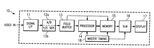
Figure 1 is a block diagram of a SLM-based display
system 10, which provides color images from pixel data
sampled from a video signal. Although the following
description is in terms of a receiver for a broA~cAct
television signal, it should be understood that receiver 10
could be any type of equipment for receiving an analog
composite video signal and displaying images represented by
the signal. Figure lA is a block diagram of a similar
system 10a, in which the image data input signal already
represents digital data. Both types of systems 10 and 10a
are referred to herein as a "digital display system~. In
both Figures 1 and lA, only those components significant to
pixel processing and bit-plane conversion are shown. Other
TI-17404 213 6 ~ 7 8 PATENT APPLICATION
components, such as those used for processing
synchronization and audio signals, are not shown.
The invention, which involves various aspects of
memory 15, is useful with either type of system 10 or lOa.
A common characteristic of both system 10 and system lOa is
that memory 15 provides data to proceCcor 14 for processing
as well as to SLM 16 for display. In other words, memory
15 integrates the functions of a pixel processing store and
a bit-plane conversion store. Thus, only one memory device
need be used in system 10 or lOa.
For ~u~o~es of example, the description herein is
directed to system lOa, and it is assumed that the
processing task to be performed by procecsor 14 is
converting interlaced fields into frames. Various de-
interlacing algorithms exist, such as line doubling, lineaveraging, median filtering, and motion adaptation. A
characteristic of typical de-interlacing algorithms is that
proce~sor 14 combines pixel data from different rows,
whether of the same field or of temporally ad~acent fields.
Examples of other processing tasks that system 10 or system
lOa is likely to perform are scaling, colorspace
conversion, and picture quality control. For each of these
tasks, processor 14 operates on pixel data. Any of these
tasks could be performed by moving pixel data back and
forth between processor 14 and memory 15 in the manner
described herein and executing a~o~iate computer
processes.
For purposes of example, an image having 768 pixels
per row, 576 rows per frame, and 8 bits per pixel is
assumed. For 8-bit pixels, the bit-length of a row is 8 x
768, or 6144 bits. In practice, a more typical pixel size
is 24 bits, with 8 bits for each of three colors. The
primary effect of different frame and pixel sizes would be
differences in the memory sizes described herein.
TI-17404 ~13 6 4 7 8 PATENT APPLICATION
As an overview of system 10, signal interface unit ll
receives an analog video signal and separates video
synchronization and audio signals. It delivers the video
signal to A/D converter 12a and Y/C separator 12b, which
convert it into a digital video signal and perform
luminance/chrominance separation, respectively. Although
the receiver 10 of Figure 1 performs A/D conversion before
Y/C separation, the order of these tasks could be reversed
for analog rather than digital Y/C separation.
A field buffer 13 is interposed between Y/C separator
12b and processor 14. This field buffer 13 is useful for
field spreading. Because the SLM-based systems 10 and lOa
do not require vertical blAnk~ng time, the extra time
between fields may be used to increase the time available
for processing data and loading bit-planes to the SLM 16.
Field buffer 13 may have other functions related to color
wheel synchronization and scaling. As indicated in Figure
1, for some tasks, such as motion adaptive de-interlacing,
data might be delivered directly from field buffer 13 to
processor 14 instead of being first written to memory 15.
Proces~or 14 prepares the data for display, by
performing various processing tasks. As stated above,
processor 14 operates on pixel data.
Memory 15 receives pixel data from field buffer 13.
At an appropriate time, memory 15 then delivers pixel data
to proce~or 14 for processing. After processing, memory
again receives the pixel data. As stated above,
transfer of data between memory 15 and proces~or 14 may be
repeated for a number of different processing tasks. After
all processing, the data is "fully proce-s~e~" in the sense
that it is ready for delivery to SLM 16. After each frame
of fully procecse~ data is stored, memory 15 delivers bit-
planes of that frame to SLM 16. Special features of memory
14 for accompli~hing both pixel data and bit-plane ouL~uL
are described below in connection with Figures 2 - 4.
TI-17404 ~ 1 ~ 6 4 7 8 PATENT APPLICATION
SLM 16 may be any type of SLM. Although this
description is in terms of a DMD type of SLM, other types
of SLMs could be substituted into system 10 or lOa and used
for the method described herein. For example, SLM 16 could
be an LCD-type SLM. Details of a suitable DMD can be found
in U.S. Patent No. 4,956,619, entitled "Spatial Light
Modulator", which is incorporated by reference herein.
Display unit 17 receives the image from SLM 16, and
provides a display image to an image plane such as a
display screen. If the system 10 or lOa handles color
data, display unit 17 may include a color wheel, which
rotates such that each bit-plane is transmitted through a
~G~Lesron~ing color filter. Master timing unit 18 provides
various system cGIlLlol functions.
lS Figure 2 illustrates processor 14 and memory 15 in
further detail. As indicated, memory 15 is a double-buffer
memory in the sense that it has a capacity of at least two
image frames. During one frame period, typically 1/60
secon~, a first area 15a stores up to one frame of data
available for processing. During the same frame period, a
secon~ area 15b stores a frame of data being loaded to SLM
16. At the end of the frame period, area 15a is filled
with a frame of data to be delivered to SLM 16, and area
15b is empty because its data has been loaded. The two
areas 15a and 15b are "ping-pong" cG"L~olled, each frame
period. After area 15b has delivered its data to SLM 16,
it becomes the area for providing data to proc~C~or 14. At
the same time, area 15a, now filled with fully proce~cse~
data, becomes the area that delivers data to SLM 16.
As stated above, memory 15 receives pixel data from
two different sources. Sometimes it receives pixel data
from field buffer 13. At other times, it receives pixel
data from procecsor 14. Dep~n~1ng on a timing function
that ~GnL~ols which source is to currently deliver data to
memory 15, multiplexer 21 directs the appropriate data to
TI-17404 ~13 ~ 4 7 8 PATENT APPLICATION
a write port 22 of memory 15. Memory 15 also has a read
port 23 for delivering data to processor 14. These ports
22 and 23 may operate concurrently, such that pixel data
may be written in while different pixel data is being read
out.
Control unit 25 receives timing signals from master
timing unit 18 and address signals from processor 14. The
data rates required for real-time image display on DMD-
based projection systems are the sub;ect of various other
patent applications, such as U.S. Serial No. 07/678,761,
incorporated by reference above. For addressing, control
unit 25 includes an address ~co~er for row-random access.
That is, any row of data may be accefise~ independently.
For example, when a field of interlaced pixel data is
written in, odd lines or even lines only may be written.
Address and control lines (not shown) are used to determine
which row is accessed.
Figure 3 illustrates a portion of memory 15,
identified as a memory unit 30. In this example, each
memory unit 30 has a capacity of 1/6 frame of pixel data.
Thus, six memory units 30 are required to store each frame
of data.
Each unit 30 has two memory arrays 34. Each array 34
has a capacity of 512 x 576 bits. This size co~Le~G.,ds to
the size of 1/12 of an image frame, and to the ability of
each of the six units 30 to store 1/6 of an image frame.
The 512 bit "height" of arrays 34 accommodates the 6144-bit
length of each row. (512 x 12 = 6144 = 8 x 768). Their
576-bit "width" corresponds to the number of rows in a
frame. It should be understood that the division of memory
15 into arrays 34 is a matter of control means and
available memory sizes. Conc~ptually, memory 15 could be
a single array having a capacity of at least two image
frames. For double buffering, the array(s) assigned to
each area 15a and 15b could share registers 31 - 33 and bit
TI-17404 213 6 4 7 8 PATENT APPLICATION
11
selector 37. Alternatively, a second set of six memory
units 30 could be used for each area 15a and 15b.
Each unit 30 also has three types of registers: input
registers 31 for receiving pixel data from processor 14,
processor-bound output registers 32 for delivering pixel
data to processor 14, and SLM-bound output registers 33 for
delivering bit-plane data to SLM 16.
Registers 31 - 33 are 256-bit registers, which
cG~Le~o-,ds to the size of 32 8-bit pixels. It should be
understood that the size of registers 31 - 33 is related to
the size of the image frames. That is, if the image has a
length of 8 x 768 bits per row, and registers 31 - 33 are
256-bit registers, a total of 24 registers are required to
store an entire row of 6144 bits. If an image frame had a
different number of rows or pixels per row, the size of
registers 31 - 33 or of arrays 34 could be ad~usted
accordingly. Likewise, the number of registers of each
type 31 - 33 in each unit 30 is related to their size and
the size of the arrays 34. If, for example, each unit 30
had only two 256-bit registers of each type, smaller arrays
34 and twice as many memory units 30 would be used.
Each memory unit 30 has four of each type of register
31 - 33, two for each array 34. Thus, where each unit 30
stores 1/6 frame, a total of 24 of each type of register 31
- 33 are used for each frame. Each array 34 is written to
and read from via two registers of each type 31 - 33. This
is another feature that ~nhAnceC data rates because top
rows can be written out while bottom rows are read in.
Parallel data lines 38 carry the data from or to registers
31 - 33 in accordance with COIILr ol signals delivered from
control unit 25.
Figure 4 illustrates the basic steps of using memory
15 in accordance with the invention. In step 41, pixel
data is written to memory 15 via input registers 31. After
each row is read to registers 31, that row it is
TI-17404 213 6 4 7 ~ PATENT AppLIcATIoN
transferred to arrays 34. In step 42, which occurs after
a sufficient amount of data is stored, typically at least
a field, pixel data is read from memory 15 to processor 14,
via registers 32. In step 43, processor 14 operates on the
data, such as by performing a de-interlacing algorithm that
creates frame data. In step 44, the proc~s~e~ data is
written to memory 15 via registers 31, in the same manner
as for step 41. If there is further processing to be
performed, steps 42 - 44 are repeated. When the data is
fully processed, it is ready for delivery to SLM 16 via
registers 33. In step 45, which occurs after at least one
frame is stored, bit-planes are read from memory 15 to SLM
16 via registers 33.
For reading data from memory 15 to SLM 16, registers
33 are controlled so that the data is received by SLM 16 in
bit-plane format. Various embodiments of memory 15 may be
used to accomplish this "format on ouLyuL" function. In
the embodiment of Figure 3, like registers 31 and 32, each
256-bit register 33 stores 8 bits for each of 32 pixels.
However, for bit-plane format, a bit selector 37 in
communication with each register 33, selects every 8th bit
of each pixel. Bit selection in this manner selects bits
0, 8, 16, ....248 from each register 33. The result is a
bit-plane of bit 0 of each pixel. Bit selector 37 then
increments one bit position to read a next bit-plane of bit
1 of each pixel. This process continues for all bit-planes
of the image. In general, for n-bit pixels, every nth bit
is selected for n bit-planes.
As an alternative to having a 256-bit capacity,
registers 33 could have a 16-bit capacity. In this case,
bit selector 37 would be placed at the input to registers
33, such that every 8th bit is loaded to registers 33.
There are a number of tech~i ques that could be used for
formatting the data into bit-planes, but an important
characteristic is that each method involves use of ouL~uL
TI--17404 2 1 3 6 g 7 8 PATENT APPLI CATION
13
registers 33 that are dedicated to delivering data to the
SLM 14 and some sort of bit selector 37 at the input or
ou~p~ of registers 33.
Typically, the loading of data into registers 31 - 33
will occur concurrently. Thus, as a row from one field is
written to registers 31, a prior row can be written to
registers 32 for delivery to processor 14, and a processing
row can be written to registers 33 for delivery to SLM 14.
S~ecial Features
Figures 5 and 6 illustrate the image data in the form
that it is stored in registers 31 - 33. As stated above,
an image having 576 rowC of data and 768 pixels per row i8
assumed. Each pixel is represented by 8 bits of data.
Each row of image data is stored as a set of blocks, each
block designated as "B - row number - block number". Where
a row of data is 768 pixels, each block is comprised of
data for 16 pixels. Thus, each block has a size of 128
bits. Each 256-bit register 31 - 33 stores two blocks of
row data in serial form.
Because each memory unit 30 has four registers of each
type 31 - 33, each memory unit 30 receives eight blocks of
data. Thus, six memory units 30 store the 48 blocks of
data that comprise each row.
A feature of many digital television systems is the
ability to display a "picture-in-picture" (PIP), which is
a small frame, usually of a decimated image from a
different signal, within the main image frame. The data
for the two frames are not necessarily in phase, and some
means must be provided so that the larger image does not
overwrite the area reserved for the small image.
Figures 7 and 8 illustrate how memory 15 may be
modified for special features, such as PIP. The data for
the special image, here a PIP, is generated using
conventional A/D conversion and decimated image generation
TI--17404 213 6 g 7 8 PATENT APPLICATION
techniques. A PIP control unit 71 controls when a PIP
image is to be displayed. If the PIP is "on", control unit
71 selects a predetermined subset of input registers 31 of
the same or of different memory units 30. These are the
input registers 31 that will receive the PIP image. For
example, block B-550-44 to block B-576-48 of one memory
unit 30 could be selected. The result is a PIP frame in
the lower right corner of the display that is four blocks
wide and 26 rows high. For a special image that is wider
than eight blocks, the registers 31 of more than one memory
unit 30 would be used.
Figure 8 illustrates a modification of the memory unit
30, designated as memory unit 80, which is used to
implement special images, such as PIP. It is like memory
unit 30, except that it is block-random rather than row-
random. A row/block ~leco~ler 81 permits data to be written
and read to selected blocks of memory 15.
During the reading of pixel data for the main image to
memory 15, conL~ol unit 29 deselects the registers 31 that
are being used for the PIP, so that the main frame is not
written to registers 31 reserved for the PIP image. Also,
registers 32 are disabled so that the PIP image data is not
delivered to processor 12 for scan conversion processing.
The control circuit of Figure 7 and the block random
access memory 80 of Figure 8 could be used for other
digital display features, such as on-screen display or
closed captioning. The registers 31 corresponding to
whatever area on the display screen is reserved for display
of special features are controlled so that the special
image is loaded to the appropriate registers 31 and not
overwritten by the main image.
TI-17404 ~13 6 ~ 7 8 PATENT APPLICATION
Other Embodiments
Although the invention has been described with
reference to specific embodiments, this description is not
meant to be construed in a limiting sense. Various
modifications of the disclosed embodiments, as well as
alternative embodiments, will be apparent to persons
skilled in the art. It is, therefore, contemplated that
the appended claims will cover all modifications that fall
within the true scope of the invention.