Note: Descriptions are shown in the official language in which they were submitted.
' '- 2~366~
INDUCTANCE ELEMENT
BACKGROUND OF THE INVENTION
In, for example, a switching power supply for
controlling a large amount of current in a high
frequency range, a choke coil has been conventionally
used to converting an AC current to a DC current or to
interrupt a high frequency component from a DC current
or an AC current of a low frequency.
On the other hand, the field to which a switching
power supply may be applied has been expanded due to a
tendency that bodies of electronic equipment are small
in size and thinner and thinner. In order to meet this
requirement and to make thin the switching power supply
itself, choke coils or the like which are components of
the switching power supply have to be made small in size
and thin.
For instance, in order to reduce a height of an
article to half an inch, a part or component, to
constitute it, that has a height (or length) of 10 mm or
less is required in view of a clearance. In other words,
magnetic parts of this type such as transformers, choke
coils and the like have not yet been made satisfactorily
low in height, and in particular, in a field where an
electric power of 10 W or more is used, there have not
been such compact components.
Furthermore, for the purpose of enhancing a heat
- 2136684
radiation efficiency of the circuit, there is a demand
to thin the overall physical size of the circuit.
Under such a circumstance, a thin type magnetic
component such as a thin type choke coil has been
realized utilizing a feature that ferrite magnetic
powder may be molded or formed into a desired shape.
However, since a saturated magnetic flux density of
the ferrite magnetic material is low in comparison with
that of a metallic magnetic material, the satisfactory
compactness has not always been attained by the ferrite
magnetic material in comparison with the choke coils
which are made of different magnetic material,
respectively, with the same performance.
In view of this point or the like, a public
attention has been paid to a technique to obtain a
compact choke coil in which a thin strip made of
amorphous magnetic alloy or crystallite magnetic alloy
having a much higher saturated magnetic flux density
than that of the ferrite magnetic material is used.
For producing such an element, a magnetic alloy
thin strip having a predetermined strip width is wound
to obtain a toroidal shaped magnetic core having a
hollow central portion with a predetermined inside
diameter, and is subjected to a suitable heat treatment.
Then, the core is received in a resin case or coated
with a resin coating. Then, a winding is effected to its
thin strip wound portion by a predetermined number of
2136689
turns.
By the way, it should be noted that, as mentioned
above, since the amorphous magnetic alloy and
crystallite magnetic alloy have a higher saturated
magnetic flux density than that of the conventional
ferrite, it is possible to obtain a compact choke coil
by these materials in comparison with the ferrite.
Since the magnetic core of the coil is obtained by
winding the above-described magnetic alloy thin strip,
in the case where the coil is constructed so that a lead
line intersects with the toroidal magnetic core, it is
necessary to decrease a width of the thin strip in order
to reduce a height of the magnetic core.
However, the reduction of the width of the magnetic
alloy thin strip makes it very difficult to wind the
strip. Namely, since the width of the thin strip is
decreased, a tension resistance of the thin strip is
decreased. When the thin strip is subjected to a
predetermined tension to be wound around the axial
center, there is a high fear that the thin strip would
be drawn and cut.
Also, the present inventors has found that even if
a thickness of the case or coating resin would be
reduced or the width of the thin strip would be
decreased in consideration of a thickness of the
winding, there is a little effect for thinning the
overall choke coil.
î A2136684 4
In view of the foregoing tasks, an object of the present invention
is to realize the compactnyess of an inductance element such as a
choke coil of this type.
SUMMARY OF THE INVENTION
The present invention relates to an inductance element, and more
particularly to an inductance element which is suitable for a choke coil
or the like to be used for smoothing a current in a switching power
supply and interrupting a high frequency component.
According to the present invention, an inductance element is
composed of a magnetic core made by winding a magnetic alloy thin
strip (ribbon) with a hollow portion along its centerline and a lead line
disposed to penetrate the central portion of the magnetic core.
Furthermore, "magnetic alloy thin strip (ribbon)" in this specification
15 means "one magnetic alloy thin strip (ribbon), magnetic alloy thin
strips (ribbons) or laminated magnetic alloy thin sheets. A relative
permeability ,u of said magnetic core is in the range of 100 to 10,000.
It is preferable that a saturated magnetic flux density Bs of the
magnetic alloy thin strip be equal to or greater than 0.6 T(Tesla).
It is preferable to select the relationship among the saturated
magnetic flux density Bsl (T) the relative permeability,u, the outside
diameter ~O(m) and the inside diameter ~j(m) of the magnetic core to
meet the following formula:
O<Bs~o/,ll~ j2<10
It is also preferable to use a thin strip of Fe-
-- ~A21 36684
- 5 -
based amorphous alloy or Fe-based crystallite alloy as the magnetic
alloy thin strip.
The "hollow portion" means a space portion formed in a central
axial portion by winding the magnetic alloy thin strip or laminating
5 magnetic alloy thin sheets, and also comprises the case where resin or
the like is filled in the spaced portion and the lead line is caused to
pass through the resin. Furthermore, the present invention includes
device which have a spacer made of ceramics may be inserted into the
spaced portion and the lead line may be inserted into the spacer.
Also, in the present invention, the magnetic alloy thin strip may
be wound directly around the lead line to form a magnetic core. In
summary, it is sufficient that the lead line is inserted into the magnetic
alloy thin strip wound in a final article condition.
Furthermore, when the magnetic alloy thin strip is wound relative
15 to the lead line, a dummy tape may be provided at a portion from
which the winding of the magnetic alloy thin strip is started.
Incidentally, it is preferable that a resistance of the lead line be
equal to or less than 20,uncm, and more preferably, it is not greater
than 2,uQcm.
An example of the amorphous magnetic alloy which is used as
the thin strip in manufacturing the inductance element according to the
present invention may be as follows:
~ ~~ 2~36684
Mloo-aM a
where M is at least one element selected from the group
consisting of Fe and Co, M' is at least one element
selected from the group consisting of B, Si, C and Cr,
and a is atomic percentage which is not smaller than 4
but not larger than 40 or the Fe-based amorphous
magnetic alloy.
The Fe-based amorphous magnetic alloy is more
preferably in the present invention.
In particular, the amorphous magnetic alloy repre-
sented by the following formula is more preferable as
the amorphous magnetic alloy which is used as the thin
strip in manufacturing the inductance element in the
present invention,
Fe~SiyBzMw
where M is at least one element selected from the group
consisting of Co, Ni, Nb, Ta, Mo, W, Zr, Cu, Cr, Mn, Al,
P, C and the like, and x, y, z and w which means atomic
percentages, and which are values that meet the
relationships, O<xc85, 5Cysl5, 5Cz~25, and 0CWC1O,
respectively.
The amorphous thin strip made of these alloys may
be adjusted in a desired composition and a desired thin
strip shape by a method which is so called the method of
rapidly querching from the melt. Also, usually, it is
possible to improve the various characteristics by
applying a suitable heat treatment thereto at a
2136684
temperature that is not lower than a Curie temperature
and not higher than a crystalline temperature.
Also, it is possible to exemplify nano-
crystalline (fine-crystalline) magnetic alloy that
constitutes the thin strip used in manufacturing the
inductance element according to the present invention,
for example as follows.
( Fel aMa )lOo-x-yM XM y
where M is at least one selected from the group
consisting of Co and Ni, M ' is at least one
element selected from the group consisting of Si, B, Ga,
Nb, Mo, Ta, W, Ti, Zr, Cr, Mn and Hf, M" is at least one
element selected from the group consisting of Cu and Al,
and a, x and y are values that meet the relationships,
O<a<0.5, O<x<50 and O~y~10 (where x and y are atomic
percentages), respectively.
The microcrystal alloy especially shown by an
undermentioned general type is desirable in the
above-mentioned alloy.
( Fel-aMa ) 100-~-y-z-a _~sixByMlzAlacu~
M is at least one selected from the group consisting of
Co, Ni. M' is at least one element selected from group
consisting of Ga, Nb, Mo, Ta, W, Ti, Zr, Cr, Mn, Hf.
Said a, x, y, z, a, and ~ are value that meet the
relationships as follows,
OsaS0.5, 0SzS25
oSXs3o~ oS ~ S10
' _ 21:3668q
O~y~25, 0~3(more preferably 0.1~ ~3)
5~x+y~z~40, o.l~a +~10
(where x, y, z, a and ~ are the atomic percentages)
It is preferable that a particle diameter of the
crystallite of the mano-crystalline alloy be not greater
than 500~, and more preferably not greater than 200~.
Also, it is preferable that the crystalline part of the
crystallite alloy is not smaller than 30~, and more
preferably not smaller than 50~.
The above-described nano-crystalline alloy thin
strips may be obtained usually by applying, to the
strips which have been once obtained as amorphous alloy
strips, a suitable heat treatment at a temperature that
is not lower than the crystallization temperature. Also,
it is possible to improve the various magnetic
characteristics (for example, permeability, iron loss or
current superposition) by changing the conditions for
the heat treatment.
It is also possible to improve the magnetic various
characteristics (for example, permeability or iron loss
in high frequency) by accumulating dielectric powder
such as MgO, SiO2, and Sb205 on surfaces of the thin
strips on one side or both sides so as to insulating the
laminated surfaces of the winding of the thin strips
from each other.
The magnetic core of the inductance element of the
present invention is produced by winding the thus
_ C A2 1 3 6684
g
obtained thin strips. first of all, the strips which have a predetermined
width and a predetermined thickness are wound around a core member
having a predetermined shape. The cross-section of the core member
may be circular or any polygonal shapes such as a rectangular shape.
At the time when the thickness of the thin strip winding portion
reaches a predetermined level, the winding operation of the thin strips
is terminated. Then, a treatment for fixing the winding end portion of
the thin strips to the magnetic core by using a highly viscous resin
tape having a heat resistance such as a polyimido (trade mark:Kapton
10 produced by Dupon chemical co.,) tape or by spot-welding is effected
so as to prevent the wind-back.
Then, the lead line is inserted into the magnetic core from which
the core member has been removed. In this case, by using the lead
line as the core member, it is possible to readily obtain an integral
15 assembly composed of the magnetic core and the lead line.
Furthermore, it is possible to dispense with the work to remove he
separate core member. This makes it possible to reduce the
manufacture cost and the number of the components. In the present
invention, it is possible to obtain the magnetic core having a hollow
20 portion by laminating troidal magnetic alloy sheet by bonding each
other with an adhesive or impregnating with a resin. This type of
magnetic core also has a hollow portion in the vicinity of the center
arranged so that a lead line may be disposed to pass therethrough.
Aluminum, aluminum alloy, copper, copper alloy, iron alloy or
25 plated surface of it for the oxidation prevention. Sn-plated copper wire
or annealed Sn-plated
2136684
- 10 -
copper wire, solder plated copper wire, 42 alloy wire,
and CP wire, etc. are enumerated as a concrete example.
Especially, the Sn-plated copper wire of the low
resistance rate is desirable in the example of the
description above.
Incidentally, for the lead line, it is possible to
arrange a plurality of conductive wires each having the
same or different cross-section in bundle along the
centerline of the magnetic core. In the case where the
plurality of conductive wires are insulated from each
other (i.e., lead lines insulated by coatings or ceramic
tubes), the conductive wires may be wound in the
longitudinal direction on the side wall of the magnetic
core to be used as a winding.
Subsequently, the magnetic core on which the thus
obtained lead line has been mounted is subjected to a
heat treatment (for controlling the magnetic
characteristics of relative permeability, for example).
Incidentally, it is possible to mount the lead line
after the heat treatment. Under the conditions of the
heat treatment, preferably, in order to keep the thin
strips in an amorphous state, the temperature is not
lower than the Curie temperature but not higher than the
crystallization temperature, and in order to keep the
thin strips in a nano-crystalline state, the temperature
is not lower than the crystallization temperature. A
period of the heat treatment is preferably ranged from
~_ Z136684
30 minutes to 24 hours. Incidentally, in this case, it
is possible to adjust the various characteristics to de-
sired ones by effecting the heat treatment while
applying a magnetic field of 0 to 60 kA/m (for example,
5 kA/m) in a width direction of the thin strip, using as
an ambient atmosphere an oxidizing gas such as nitrogen
(N2) or Argon (Ar), a reducing gas or an inert gas, or
applying a force to the magnetic core in a constant
direction.
Thereafter, the magnetic core is encased in a case
or is subjected to an insulation with resin ( for
example, epoxy resin, polyester resin, or silicon resin)
coatings for obtaining the inductance element according
to the present invention.
In the element of the present invention, for obtain
the good characteristic of current superposition, the
relative permeability ,u of the magnetic core at an
original point on a magnetizing curve at 100 kHz has to
meet the following relationship:
lO0C~'10,000
Inductance element of the present invention is used
as smoothing choke coil, a choke coil for an alternating
current line, choke coil for an active filter, choke
coil for switching converter or noise reduction element
and the like.
Now, it is preferable that, in order to obtain a
good superposition characteristic in case of a smoothing
- 2136684
choke coil or a choke coil for an alternating current
line, a choke coil for an active filter, and/or a choke
coil for a switching converter the relative permeability
,u of the magnetic core meet the relationship:
100S~<2,000.
More preferably, by adjusting the heat treatment
conditions so that the specific magnetic permeation
meet the relationship, 500s~s2,000, the current
superposition characteristic becomes more excellent.
On the other hand, it is preferable that, in order
to obtain a satisfactory noise reduction performance in
case of a noise reduction element, the relative
permeability ,u of the magnetic core meet the
relationship: 5, OOO<~S10, 000.
Incidentally, the relative permeability ,u means a
value obtained by dividing the permeability ~i by the
vacuum permeability ~u0.
- On the other hand, the compactness of the magnetic
components largely depends upon the saturated magnetic
flux density. Namely, assuming that the relative
permeability ,u is kept constant up to the saturated mag-
netic flux density Bs~ the following relation between
the electric capacitance E of the magnetic component and
the volume V of the magnetic core is given:
E ~ (Bs)V/(,u)
In order to obtain the compact magnetic component which
has been widely and generally used and which has a
- '- 2136684
- 13 -
larger capacity than that of the ferrite magnetic
material, it is preferable that the saturated magnetic
flux density of the magnetic alloy thin strip be not
smaller less than 0.6 T.
In this invention, when design the outer diameter
~0(m:meter) and inner diameter ~i(m) of magnetic core,
the saturation magnetic flux density Bs (T:tesla), ~0,
~i, relative permeability ~, vacuum permeability ~0
(4~X10~7H/m) and maximum electric current density u of
lead wire will fill the following relational expression
is desirable.
Bs950/~ ~0~ (J ¢li2/4
A large capacity and small magnetic parts are
obtained by designing the element which satisfies the
above-mentioned relational expression.
Said relational expression is transformed as fol-
lows:
B8~0/ ,U(¦~i2<,UoCJ/4
Also, in consideration of the conditions for
realizing the magnetic core, i.e., ~0, ~i>0, the
following condition is given:
O<Bs~O/ll~i2~1l0a/4
The present inventors have found that, in order to
suppress the amount of heat generated in the element, it
. is preferable that the current density a be not greater
than ~ =100/~xlOfiA/m2 (about 32xlO6A/m2). Accordingly, by
the substitution of a=100/~xlO6A/m2, the following
213668~
- 14 -
relation is obtained among the saturated magnetic flux
density ~s of the magnetic core, the relative
permeability ~, the outside diameter ~O(m) and the
inside diameter ~i(m) of the magnetic core:
O<Bs~o/~u~i2< 1 0
According to the present invention, the element
meets the relation, i.e., O<Bs~o/~iZ'10, and more
preferably meets the relation, i.e., O.l<Bs~o/~i2<10
where Bs(T) is the saturated magnetic flux density of
the magnetic core, ~ is the relative permeability, ~O(m)
is the outside diameter of the magnetic core and ~i(m)
is the inside diameter of the magnetic core, whereby it
is possible to obtain an element which suffers from a
less temperature elevation even if it is made compact as
an actual element.
Also, it is preferable that the resistance of the
lead line to be used in the present invention be not
greater than 20,uQcm, and more preferably not greater
than 2 ,uQcm. Namely, if the resistance of the lead line
is not greater than 20~Qcm, it is advantageous that the
temperature elevation is suppressed. Furthermore, if the
resistance of the lead line is not greater than 2~Qcm,
it is further advantageous that the temperature
elevation is further suppressed.
The inductance element may be encased in a case
made of non-magnetic material such as synthetic resin or
aluminum or otherwise may be sealed by epoxy resin or
2136684
- 15 -
the like. It is possible to enhance the heat radiation
characteristics by providing fins, which are made of
non-magnetic material such as aluminum, to the outside
of the package, i.e., case in the case where the outer
configuration of the package is in the form of fins or
the package is made of synthetic resin.
Polyamide (nylon), modified polyamide (Trade Name :
ARLEN made by Mitsui Petrochemical Co., Ltd.), PBT
(polybutylene terephthalate), PET (polyethylene
terephthalate), PPS (polyphenylene sulfide) and PP
(polypropylene) etc. can be mentioned as plastic which
can be used as a material of the case.
Furthermore, it is possible to obtain elements
having difference inductance and current by connecting a
plurality of thus obtained inductance elements in paral-
lel or in series with each other. In this case, it is
possible to obtain versatile elements with a uniform
outer appearance without changing a height of the
element, for example, by sealing the elements with epoxy
resin or the like to form the package in a single
assembled element unit after arranging the individual
inductance elements in parallel.
Incidentally, these inductance elements may be
encased in a case made of synthetic resin to form a
single assembled element. In case of such an assembled
element, since the heat generation amount is also
increased, the outer appearance of the case should be in
- -- 2136684
the form of fins or the non-magnetic material such as
aluminum should be disposed outside the package to
thereby obtain the inductance assembly unit that is
superior in heat radiation property.
Of a method for connecting the plurality of
elements, it is possible to encase the elements that
have been connected in advance or to seal them by epoxy
resin, or otherwise to connect the elements by utilizing
a print wiring or the like on the actually installed
substrate.
It is possible to handle or use the elements
according to the present invention in the same way as
for the various elements such as a capacitance, a
resistor and the like. Because no-winding in the element
itself, the elements according to the present invention
are easy to handle and compact in size.
BRIEF DESCRIPTION OF THE DRAWINGS
In the accompanying drawings:
Fig. 1 is a perspective view showing an inductance
element according to the present invention;
Fig. 2 is a cross-sectional view showing the
inductance element according to the present invention;
Fig. 3 is a front view showing the inductance
element according to the present invention;
Fig. 4 is a perspective view showing an assembled
element which is formed by arranging a plurality of
- 2136684
- 17 -
inductance elements of the present invention in
parallel;
Fig. 5 is a perspective view showing a toroidal
choke coil according to a comparison example;
Fig. 6 is a cross-sectional view showing the
toroidal choke coil according to the comparison example;
Fig. 7 is a perspective view showing a state in
which a thin strip is directly wound on a lead line in
the inductance element according to the present
invention;
Fig. 8 is a perspective view showing the inductance
element according to the present invention, in which a
case is made in the form of fins;
Fig. 9 is a perspective view showing an inductance
element representative of a modification of the lead
line;
Fig. 10 is a graph showing a current superposition
characteristic of an inductance obtained by the
embodiment of the present invention and the comparison
example;
Fig. 11 is a perspective view showing an outer
appearance of an assembled element according to an
example 2 of the present invention; and
Fig. 12 is a perspective view showing an outer
appearance of an assembled element according to a
modification of the example 2 of the present invention.
'-- 2136~84
- 18 -
DESCRIPTION OF THE PREFERRED EMBODIMENTS
The present invention will now be described with
reference to the accompanying drawings.
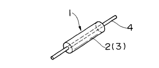
As shown in Fig. 1, according to the present
invention, a magnetic core 2 for an inductance element 1
is manufactured by winding a thin strip 3 which has been
obtained as mentioned above. First of all, the thin
strip that has a predetermined width and a predetermined
thickness is wound around a core member (not shown)
having a preselected shape. The cross-section of the
core member is not limited to a circular shape but may
be rectangular or polygonal.
At the time when the thickness of the wound portion
of the thin strip reaches a predetermined level, the
winding operation of the thin strip 3 is terminated. A
treatment to fix the wound end portion of the thin strip
3 to the magnetic core 2 by using a highly viscous resin
tape having a heat resistance such as a polyimido (Trade
name: Kapton) tape or by spot-welding is effected so as
to prevent the wind-back.
A lead line 4 is inserted into the magnetic core 2
from which the core member has been removed. In this
case, as shown in Fig. 7, by directly using the lead
line 4 as the core member, it is possible to readily
obtain an integral assembly composed of the magnetic
core 2 and the lead line 4. Furthermore, it is possible
to dispense with the work to remove the separate core
213668~
-- 19 --
member. This makes it possible to reduce the manufacture
cost and the number of the components.
Aluminum, aluminum alloy, copper, copper alloy,
iron alloy or plated surface of it for the oxidation
prevention. Sn-plated copper wire or annealed Sn-plated
copper wire, solder plated copper wire, 42 alloy wire,
and CP wire, etc. are enumerated as a concrete example.
Especially, the Sn-plated copper wire of the low
resistance rate is desirable in the example of the
description above.
Incidentally, for the lead line 4, it is possible
to arrange a plurality of conductive wires 4a each
having the same or different cross-section in bundle
along the centerline of the magnetic core 2. In the case
where the plurality of conductive wires are insulated
from each other (i.e., lead lines insulated by coatings
or ceramic tubes), the conductive wires may be wound in
the longitudinal direction on the side wall of the
magnetic core to be used as a winding as shown in Fig.
9.
Subsequently, the magnetic core 2 on which the thus
obtained lead line 4 has been mounted is subjected to a
heat treatment. Incidentally, it is possible to mount
the lead line after the heat treatment. Under the
conditions of the heat treatment, preferably, in order
to keep the thin strips in an amorphous state, the
temperature is not lower than the Curie temperature but
_ 2136684
- 20 -
not higher than the crystallization temperature, and in
order to keep the thin strips in a nano-crystalline
state, the temperature is not lower than the
crystallization temperature. A period o~ the heat
treatment is ranged from 30 minutes to 24 hours.
Incidentally, in this case, it is possible to adjust the
various characteristics to desired ones by effecting the
heat treatment while applying a magnetic field of 0 to
60 kA/m (for example, 5 kA/m) in a width direction of
the thin strip, using as an ambient atmosphere an
oxidizing gas, a reducing gas or an inert gas, or
applying a force to the magnetic core in a constant
direction.
The inductance element l may be encased in a case
made of non-magnetic material such as synthetic resin or
aluminum or otherwise may be sealed by epoxy resin or
the like. In this case, as shown in Fig. 8, it is
possible to enhance the heat radiation characteristics
by providing fins, which are made of non-magnetic
material such as aluminum, to the outside of the
package, i.e., case 18 in the case where the outer
configuration of the package is in the form of fins or
the package is made of synthetic resin.
Furthermore, it is possible to obtain elements
having difference inductance and current by connecting a
plurality of thus obtained inductance elements l in
parallel or in series with each other. In this case, it
'- 21366~4
is possible to obtain versatile elements with a uniform
outer appearance without changing a height of the
element, for example, by sealing the elements with epoxy
resin or the like to form the package 5 in a single
assembled element unit 6 after arranging the individual
inductance elements 1 in parallel as shown in 4.
Incidentally, although the plurality of inductance
elements 1 are sealed by resin in Fig. 4, these
inductance elements 1 may be encased in a case made of
synthetic resin to form a single assembled element. In
case of such an assembled element, since the heat
generation amount is also increased, the outer
appearance of the case should be in the form of fins
which are similar to those shown in Fig. 8 or the non-
magnetic material such as aluminum should be disposedoutside the package to thereby obtain the inductance
assembly unit that is superior in heat radiation
property.
Of a method for connecting the plurality of
elements 1, it is possible to encase the elements that
have been connected in advance or to seal them by epoxy
resin, or otherwise to connect the elements by utilizing
a print wiring or the like on the actually installed
substrate.
Specific Examples of the present invention and
Comparison Example will now be described.
2136684
- 22 -
Example 1
As shown in Fig. 7, a surface (one sided) of a Fe-
based amorphous magnetic alloy thin strip 3 (Trade
Name: "Metglas 2605S-2", composition: Fe7,3SigBl3(atom ~),
thickness: 20 ,um, width: 15 mm) made by US Allied-signal
Inc. was coated with fine powder of SbzOs, and thereaf-
ter, the strip was wound around a lead line 4 which
annealed Sn-plated copper wire (resistivity: 0.97~Qcm)
having a diameter of 1.6 mm to form an element 1 having
an inner diameter of 1.6 mm, an outer diameter of 5 mm
and a length of 15 mm.
The winding end was fixed by polyimido tape (Kapton
tape). This was exposed in an N2 atmosphere and heated
at a temperature that was not lower than Curie
temperature and not higher than crystallization
temperature. Specifically, the condition of heat
treatment was 430C and time-length in 2 hours.
Five elements each of which was produced as
described above were arranged in parallel and sealed by
epoxy resin 5 to form a package body, and terminals
(lead lines 4) were projected from one side of the
package body so as to be mountable on the print circuit
board, thus producing an assembled element 6. The outer
appearance thereof is shown in Fig. 4.
The terminals were electrically short-circuited so
that the five elements 1 were connected in series in the
package body, and the current superposition
213668~
-
- 23 -
characteristic of the inductance was measured at a
frequency of 100 kHz.
Example 2
As shown in Fig. 7, a Fe-based amorphous magnetic
alloy thin strip (Trade Name: "Metglas 2605S-2", compo-
sition: Fe78SigBl3(atom %), thickness: 20 ~um, width: 15
mm) made by US Allied-signal Inc. was wound around a
winding core having a diameter of 1.6 mm, and after the
completion of the winding, the end portion was fixed by
spot-welding. Thereafter, the winding core was removed.
After that, the magnetic core which having an inner
diameter of 1.6 mm, an outer diameter of 5 mm and a
length of 15 mm was obtained. This was exposed in an N2
atmosphere and heated at a temperature that was not
lower than Curie temperature and not higher than crys-
tallization temperature. Specifically, the condition of
heat treatment was 430C and time-length in 2 hours.
An annealed Sn-plated copper wire (resistivity:
0.89~Qcm) that had been shaped into a U-letter in
advance was inserted into the article and was reshaped
into a lead line 14 by a pressing machine.
The produced article was encased in a case 15 made
of modified polyamide (Trade Name: ARLEN) made by Mitsui
Petrochemical Co., Ltd. and the case 15 are fixed to
each other with epoxy system adhesives. The outer ap-
pearance is shown in Figs. 11 and 12.
-- 2136684
- 24 -
Comparison Example
On the other hand, in comparison, a toroidal choke
coil 11 (TM coil 6,uH-lOA) having the same rated
capacitance was produced as shown in Figs. 5 and 6.
In the same manner as in Example 1, a surface (one
sided) of a Fe-based amorphous magnetic alloy thin strip
(Trade Name: "Metglas 2605S-2", composition: Fe78SigBl3,
thickness: 20 ~m, width: 5 mm) made by US Allide-Signal
Inc. was wound to a magnetic core 12 having an outside
diameter of 21.5 mm and an inside diameter of 12.0 mm.
The winding was subjected to a heat treatment and was
received in the resin case 15. Thereafter, two lead
lines 16 each having a diameter of 1.1 mm were wound in
parallel by eight turns about a circumferential
direction of the case 15 made of resin. As a result, a
toroidal choke 11 having an outside diameter (Q) of 27
mm and a height (h) of 12 mm was obtained.
With respect to this toroidal choke coil, the
current superposition characteristic of the inductance
at the frequency of 100 kHz was measured (Comparison
Example). Fig. 10 shows a change in inductance relative
to the superposition current between the Example and the
Comparison. The following Table shows the comparison in
package dimension between Examples and Comparison.
Z136684
- 25 -
Ex. 1 Comparison 1 Ex. 2
rated capaci- 6~H-lOA 6yH-lOA 4~H-5A
tance
actual dimen- a=25 mm, Q = 27 mm a=13 mm,
sion b=20 mm b=20 mm
actual height 6 mm 12 mm 7 mm
foot print 500 mm2 729 mm2 260 mm2
weight 10 g 15 g 5 g
relative 500 250 1,000
permeability
( ~ )
B~ 1.56 T 1.56 T 1.56 T
~n 5~10~3m 5.0 mm
~; 1.6~10~3m 1.6 mm
~ 4.97xlO6A/m2 5.26xlO6A/m2 4.42xlO6A/m2
Bs~o/Y~i 6.09 - 3.05
temperature
rise(~C) in
rated cur- 26.2C - 9.8~C
rent(DC)
Thus, according to the examples, the foot print was
small in comparison with the conventional article, and
the actual height was about half of the conventional
article.
Various details of the invention may be changed
without departing from its spirit nor its scope.
Furthermore, the foregoing description of the
embodiments according to the present invention is
provided for the purpose of illustration only, and not
for the purpose of limiting the invention as defined by
'_ 213668~
- 26 -
the appended claims and their equivalents.