Note: Descriptions are shown in the official language in which they were submitted.
'=i'0 93/24992 213 6 7 6 0 PCT/US93/04777
1
-1-
DIGITAL TRANSDUCER SYSTEM
Background of the Invention
1. Field of the Invention
The present invention applies generally to
variable reluctance transducers employing parallel
resonant circuits producing signals for manipulation to
represent the input to the transducer with an output
value. Specifically, the present invention employs
digital control of parallel resonant circuits
incorporating variable reluctance elements acting as
the force sensor in the transducer providing dual
frequency signals for digital calculation to obtain a
quotient of the frequencies thereby substantially
eliminating the resonant frequencies as a variable in
accuracy of the device. Manipulation of the produced
quotient through digital calibration tables responsive
to a temperature sensor produces an output value which
substantially eliminates temperature-induced errors in
the system and further increases accuracy.
2. Prior Art
Variable reluctance transducers have been in
use for a number of years in the measurement of
physical parameters which can be resolved into force on
a diaphragm. Displacement or deformation of the
diaphragm due to the force which may be fluid pressure,
acceleration or other physical phenomenon exerted on
the diaphragm provides a basis for measurement. An
WO 93/24992 PCT/US93/0'
-2-
1 - inductor or capacitor mounted to the diaphragm changes
value based on the displacement or deformation.
Incorporation of the inductor or capacitor in a
resonant circuit allows measurement of the deformation
by change in frequency. The use of two variable
reluctance elements to produce two separate frequencies
based on deformation of the diaphragm provides a basis
for calibrating and correct.~ng the measured value.
Integration of both variable reluctance elements with
the diaphragm to produce opposite variation of the
parameter value or fixed mounting of one element for
comparison with the element mounted to the diaphragm
allows calibration through various combinations of the
two frequencies produced. U.S. Patent No. 3,140,450
entitled "Force Controlled Variable Reactance
Transducer," issued on July 7, 1964 to the inventor of
the present application discloses the structure of such
a transducer wherein the frequencies produced by the
two resonant circuits are mixed to obtain a difference
frequency for measurement of the force applied to the
diaphragm.
Calibration and compensation of variable
reluctance transducers has been accomplished in the
prior art through the design of the oscillator circuit
provided to drive the variable reluctance resonant
circuit of the transducer. Various means to provide
constant amplitude signals for increased accuracy of
measurement are disclosed in various prior art patents
such as U.S. Patent Nos. 3,763,444, 3,837,227 and
4,947,139, all issued to the inventor of the present
application.
While significant accuracy improvements have
been made in variable reluctance transducers, the
inaccuracies caused by nonlinearity in deformation
characteristics of the diaphragm, influence of
temperature on the diaphragm characteristics and
electronic components, and conversion of the data
r r T
._. WO 93/24992 _ ~ ~ ~ ~ ~ ~ ~ PCT/US93/04777
-3-
1 produced by the transducer to usable form continue to
require creative solutions.
The present invention provides a novel
oscillator circuit for control of switchable dual
resonant circuits for a variable reluctance transducer
in combination with a digital control system for
accurate conversion of the raw transducer signal and to
provide a digital output of desired form allowing easy
analysis and manipulation of the data produced.
Summary of the Invention
The digital transducer system of the present
invention receives a force input on the diaphragm of
the transducer. A first resonant circuit incorporating
either a variable inductor or a variable capacitor is
activated by a first control signal producing a first
frequency dependant on the force input to the
transducer. A second resonant circuit incorporating a
variable or fixed element comparable to the first
resonant circuit is activated by a second control
signal to produce a second resonant frequency. If the
element in the second resonant circuit is variable, the
second frequency is similarly dependent on the
transducer force input. A microcontroller is employed
to produce the first and second control signals. The
control signals are asserted on a mutually exclusive
basis to allow use of a common resonant element by the
two resonating circuits. The microcontroller also
incorporates a frequency measurement circuit connected
to the first resonating circuit and second resonating
circuit for measurement of the ffirst resonant frequency
and second resonant frequency when activated by the
first and second control signal respectively. The
microcontroller divides the first frequency by the
second frequency to create a quotient representative of
the force on the transducer and calculates a raw
parameter based on the quotient. A table lookup
WO 93/24992 PCT/US93/0~!
X1367 60
-4-
1 conducted by the microcontroller in a programmable
read-only memory based on the raw parameter value
provides a calibrated value for the parameter measured
by the transducer. Use of a lookup table for
calibration allows compensation for nonlinearities in
the diaphragm, and a temperature sensor is employed to
provide input to the micro.cdntroller for use in
combination with the raw parameter data to produce the
input parameter employed by the microprocessor for the
lookup table.
Control of the resonant circuits is provided by an
oscillator circuit incorporating an amplifier receiving
an output from the first and second resonant circuit as
an input and providing the output of the resonant
frequency to the microcontroller. The output of the
amplifier is also provided to a detector for conversion
to a DC signal which is compared to a reference voltage
through a diode chopper operating at the oscillator's
frequency. The signal generated by the chopper is
returned as a feedback signal to the resonant circuits
to maintain the oscillation. The feedback signal is
proportional to the difference between the detected
signal and the reference voltage.
30
~ _~.
WO 93/24992 PCT/US93/04777
.213676
-5-
1 Description of the Drawing's
The features of the present invention may be more
clearly understood by description with reference to the
following drawings.
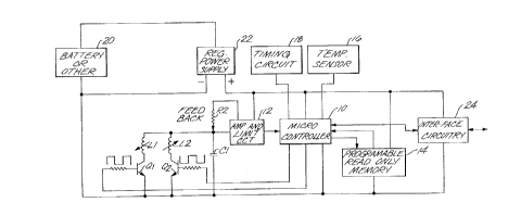
FIG. 1 is a block diagram showing the
interrelationship of the elements of the present
invention, and
FIG. 2 is a schematic diagram of the oscillator
control circuit for the present invention.
15
25
35
WO 93/24992 PCT/US93/04~
-6-
~zi3s~ so
1 Detailed Description
Referring to FIG. 1, a force gauge is created by
placing two inductive sensors L1 and L2 on each side of
a flat diaphragm (not shown). The inductance of each
sensor is inversely proportional to the distance from
a front open face to the diaphragm, thereby creating a
variable inductor. A force applied to one side of the
diaphragm, such as a fluid pressure, will cause the
diaphragm to deform, moving toward one sensor and away
from the other sensor. Inductance of one sensor is
thereby increased, while inductance of the other sensor
is decreased. A capacitor C1 is connected across the
variable inductors to form a resonant circuit with each
inductor. A switching transistor Q1 is inserted in the
first resonant circuit with inductor L1, and a
switching transistor Q2 is inserted in the circuit with
inductor L2. Turning transistor Q2 off and transistor
Q1 on allows the first resonant circuit to oscillate
while disabling the second resonant circuit. Switching
transistor Q1 off and transistor Q2 on conversely
allows the second resonant circuit to oscillate.
Alternate embodiments of the present invention
employ variable capacitors associated with the
diaphragm and a fixed single inductor as a replacement
for capacitor C1 to form the resonant circuits. In
addition, a fixed value component may be substituted
for one of the variable components in one of the
resonant circuits to provide a fixed frequency
reference for the variable frequency resonant circuit.
The gate of transistor Q1 is connected to a first
control signal provided by a microcontroller 10 while
the gate of transistor Q2 is connected to a second
control signal from the microcontroller. The
microcontroller asserts the first and second control
signals alternately for activating the first and second
resonant circuit. This allows a single capacitor to be
used as the second element of both resonant circuits,
WO 93/24992 , ~ ~ ~ ~ ~ 6 O PCT/US93/04777
1 thereby increasing the accuracy of the transducer.
The two resonant circuits are connected through an
amplifier and limit circuit 12 which provides control
of the oscillator alternately formed with each of the
two resonant circuits. Feedback from the amplifier and
limit circuit through resistor R2 maintains the
oscillation and controls the amplitude of the
oscillation. The frequency of the active resonant
circuit is provided from the amplifier and limit
circuit to the microcontroller. A counter in the
microcontroller determines the frequency of the
selected resonant circuit which is stored by the
microcontroller. Alternating of the first and second
control signals allows frequencies for both resonant
circuits to be determined. The microcontroller
calculates the quotient of the frequencies of the first
and second resonant circuits. Using pressure as an
example of the parameter measured by the transducer,
the frequency of the first resonant circuit F1 and the
frequency of the second resonant circuit F2 are defined
by the equations
F1 - 1/ (2*~r* (L1*C)'~=
F2 - 1/ (2*~r* (L2*C)''=
L1 - K G1 L2 - K G2
where L1 is the inductance of inductor L1, and L2 is
the inductance of inductor L2. K is a numerical
constant, and G1 is the air gap between the diaphragm
and the first inductor, and G2 is the air gap between
the diaphragm and the second inductor.
If GO equals the initial air gap, then
G1 = GO+N*GO = GO(1+N)
G2 = GO-N*GO = GO(1-N)
where N is the per unit motion of the diaphragm's
initial air gap GO and N is proportional to the
pressure P which is applied to the diaphragm. K1 is a
second numerical constant. Taking the quotient of the
frequencies and substituting from the above equations,
WO 93/24992 PCT/US93/OS
~7 6~
1 the value for capacitance drops out of the equations
and
L1/L2 - G2/G1
- (1-N)/(1+N)
F1/F2 - (L2/L1)''=
- ((1+N)/(1-N))'''-
(F1/F2)z - (1+N)/(1-N)
N - ( (F1/F2)'--~) / ( (F1/F2)z+1)
therefore, an equation for the raw pressure data is
p - (1/K1)*((F1/F2)2-1)/((F1/F2)z+1)
Variation of the linearity in the diaphragm and
changes in capacitance and inductance due to
temperature of the circuits is compensated in the
present invention through the use of lookup tables
stored in a programmable read-only memory 14. A
temperature sensor 16 located adjacent the diaphragm
provides temperature data to the microcontroller. The
raw pressure data is combined with the temperature data
in the microcontroller to provide a value for the
lookup table. Interpolation between calibration points
in the matrix stored in the lookup table is made by the
microcontroller. Use of the calibration matrix in the
lookup table compensates for temperature,
nonlinearities of the diaphragm at large excursions,
imperfect inductors, leakage flux and any current
losses and nonlinearities of the circuit. By solving
the equation for the raw pressure data in the
microcontroller, the interpolative intermediate points
in the calibration matrix are much closer. A minimum
of calibration input data significantly improves the
accuracy of the transducer over direct conversion of
the raw pressure data to a calibrated pressure output.
A calibration matrix for an embodiment of the
present invention comprises approximately 5 to l0
pressure data points taken over 5 or 10 temperatures
between -55°C to +150°C. This produces a three-
'U~93/04777
~1~b76(~ IPEAlUS 21 GEC ~~93
_g_
dimensional matrix of approximately 25 to 100 discrete
data points. The microprocessor selects points in the
calibration matrix based on the raw input from the
transducer and the input from the temperature sensor.
Interpolation between the two points performed by
calculation in the microcontroller provides the final
data output value. Linearity between the points in the
matrix is required for the best accuracy of the system;
however, no requirement is present that the points in
the calibration matrix be at equally spaced values.
Consequently, for example, in compensating for
nonlinearities in the diaphragm, widely spaced points
may be used through the region of limited displacement
of the diaphragm, with spacing of calibration points in
the matrix becoming increasingly closer in value at
extended distances of travel .or deformation of the
diaphragm.
Control of the resonant circuits to provide a
constant amplitude signal to the microprocessor is
accomplished in the amplitude and limit circuit 12. As
best seen in FIG. 2, the parallel resonant circuits
provide an output which is connected to amplifier U1.
The output of amplifier U1 is provided through a second
stage comprising transistors Q3 and Q4 to the
microcontroller. The second stage of the amplifier
provided by transistors Q3 and Q4 provides a squaring
circuit for the sine wave output produced by amplifier
U1. The square wave input provides more accurate
triggering of the counting circuits in the
microcontroller.
The output of amplifier U1 also is provided to
transistor Q5 for detection of the signal level.
Transistor Q6 provides a reference for detection of the
signal from the resonant circuits. Resistors R7 and R8
establish the reference level at approximately 2.5 VDC
for a ~5-volt system. Resistors R4 and R5 provide
negative feedback for control of the gain of amplifier
AME~~f D SHEET
PCT~U~ 9 3 / 0 ~ 7 7 7
213676Q IPEI~~ 2~ ~~C 1993
-10-
U1. Resistor R3 drives the resonant signal through
capacitor C2 into chopper diodes CR1 and CR2. A
positive AC signal from the resonant circuit results in
conduction by CR2 at the voltage established by
transistor Q6. A negative AC signal causes diode CR1 to
conduct limiting the feedback signal provided through
resistor R2 to the resonant circuit. At small
oscillation amplitudes in the resonant circuit, the
feedback signal through resistor R2 as driven by the
reference transistor Q6 is large due to a lack of a
substantial DC level on the signal output from amplifier
U1. As the oscillation amplitude increases in the
resonant circuits, .the feedback is reduced to a level
only sufficient to maintain oscillation when the
detected signal from amplifier U1 is substantially equal
to the reference voltage.
Diodes CR3 and CR4 are provided on the emitter of
transistor Q6 for temperature compensation. Capacitors
C3 and C4 provide filtering for the circuit. Resistor
R6 is the load resistor for transistor Q6.
In a preferred embodiment of the present
invention, the microcontroller employed is a National
Semiconductor COP888CGMH single chip micro CMOS micro
controller. This device incorporates an erasable,
programmable, read-only memory (EPROM) on the single
chip with the microcontroller. As shown in FIG. 1, a
timing circuit 18 comprising a crystal oscillator
provides basic clocking for the microcontroller. Power
for the transducer system is provided by a battery or
other power source 20 through a regulated power supply
22.
Incorporation of the microcontroller in the
present invention allows great flexibility for the
applications in which the invention is used. The
microcontroller provides a digital output corresponding
to the corrected and calibrated transducer value for
pressure or other measured parameter. This value is
a, ', ~'~.v r
~.v;~n~~_~ SH~tT
2I~67so
WO 93/24992 - PCT/US93/04777
-11-
1 provided through standard interface circuitry 24 to
data acquisition or transmission devices.
The interface circuitry provides communication
with the sy~~em through standard serial interfaces or
an SDI 12 which is incorporated within a telemetry
system for control of the digital transducer system and
transmission of data from the system. The format of
the data output from the digital transducer system is
determined by the programming of the microcontroller.
Calculations based on the raw input data can be
manipulated from a pressure input as an example to a
flow input based on pressure drop in a venturi tube.
Such an application may be used for water flow rate or
air speed. Raw pressure data may be converted to
altitude information or barometric pressure at fixed
altitude for weather measurement. Incorporation of
time into the equation through the timing circuit used
with the microcontroller allows calculation of
additional variable rates of pressure change such as a
variometer for rate of climb or descent.
As exemplary of an implementation of the system,
the digital transducer system in combination with an
SDI 12 system with telemetry from a satellite
connecting to central ground control is mounted in a
self-contained package including a battery for
operational power. Control of the entire system by the
microcontroller allows maintaining of the system in a
stand-by mode for minimum power consumption until
telemetered "wake-up" instructions are received through
the SDI 12 system. The microcontroller activates the
transducer by application of the first and second
control signals to obtain data, as previously
described, which is then provided to the SDI 12 system
for telemetry to the satellite and hence the central
ground control. Interrogation of the system is only
required for one second or so, thereby providing
significant potential life for operation. Use of this
WO 93/24992 PCT/US93/04'
2136760
- -12-
1 system in a pressure-measurement application can
provide pressure measurement in lakes and, by way of
calculated flow rate based on static pressure, the flow
of streams in remote areas. The information obtained
from remote locations is telemetered through the
satellite to a central location for analysis. A
simple, cost-effective, stan.d~.alone system is obtained.
Having described the: invention in detail as
required by the patent sta-tutes, those skilled in the
art will recognize alterations and substitutions for
the elements of the inventions for specific
embodiments. Such modifications and substitutions are
included within the intended scope of the invention as
defined by the following claims.
20
30