Note: Descriptions are shown in the official language in which they were submitted.
CA 02136886 2006-12-15
1
APPARATUS, SYSTEM AND METHOD FOR REAL-TIME WAFER
TEMPERATURE MEASUREMENT BASED ON LIGHT SCATTERING
TECHNICAL FIELD OF THE INVENTION
The present invention relates in general to
real-time measurement of semiconductor wafer physical
characteristics, and more particularly to a method and
apparatus for non-invasive semiconductor wafer
temperature measurements based on surface roughness
induced scattering of laser beams.
2136886
TI-15257 PATENT APPLICATION
(32350-762)
2
BACKGROUND OF THE INVENTION
Integrated circuit chip manufacturers fabricate
semiconductor devices by different combinations of
fabrication processes. Wafer temperature is an important
parameter for many of these processes. More
specifically, precise measurement and control of wafer
temperature and its uniformity are required in order to
minimize deviations from the target process parameters
and increase device fabrication yield. Thermal
fabrication processes, such as thermal anneals,
oxidation, and chemical vapor deposition (CVD) are
examples of processes where wafer temperature is an
important process parameter. Currently, thermocouples
are used to measure wafer temperature during plasma etch
operations such as reactive ion etch (RIE).
Additionally, some chemical vapor deposition processes,
such as plasma-enhanced chemical vapor deposition (PECVD)
employ thermocouples for temperature measurement.
Thermocouples for measuring temperature in
semiconductor fabrication equipment have substantial
disadvantages. For instance, thermocouples can be
disturbed by the RF and electromagnetic fields (e.g.,
13.56 MHz RF and 2.45 GHz microwave) used to generate
plasma during plasma etch processing. Thermocouples are
also invasive in that they must be placed very near the
location where the temperature is being measured. In
some applications the thermocouples may require actual
contact with the wafer surface for accurate temperature
sensing, thereby causing disturbance of the wafer
temperature and also possible wafer contamination.
Furthermore, most thermocouples suffer from measurement
error and slow response time problems.
Pyrometry providing for non-contact operation can
also be used to measure wafer temperature in some thermal
TI-15257 2t368" " PATENT APPLICATION
(32350-762)
3
processing applications such as rapid thermal processing
(RTP). Computational pyrometry sensors, however, have
several disadvantages. For example, for accurate
pyrometry-based temperature measurements, an accurate
knowledge of the spectral emissivity of the wafer at the
pyrometry measurement wavelength band is required. It is
known that spectral emissivity can vary with various
parameters, such as wafer ternerature, wafer resistivity,
material layers, and their thickness, and process chamber
geometry and materials, making pyrometry sensors
relatively inaccurate due to emissivity variations and
other noise sources. In general, conventional pyrometry
techniques can suffer from measurement inaccuracies and
repeatability errors as high as 100 C or more.
Moreover, pyrometry techniques require frequent cross-
calibrations using thermocouples introducing the problems
associated with thermocouples noted previously.
TZ-15257 no
PATENT APPLICATION
(32350-762)
4
SUMMARY OF THE INVENTION
Therefore, a need has arisen for a method and
apparatus for accurate and repeatable measurement of the
temperature of a semiconductor wafer during device
fabrication processing.
A need exists for a wafer temperature sensor which
is not affected or disturbed by RF and electromagnetic
fields which may be present during wafer processing.
A need further exists for a wafer temperature sensor
which is non-invasive to the semiconductor wafer process.
A further need exists for a wafer temperature sensor
which is not susceptible to error and slow response.
A need further exists for a wafer temperature sensor
which does not depend on knowledge of spectral emissivity
of the wafer to determine its temperature.
Yet a further need exists for a wafer temperature
sensor which does not require cross-calibrations with
additional temperature sensors.
In accordance with the present invention, a method,
system and apparatus are provided which substantially
eliminate or reduce disadvantages and problems associated
with prior wafer temperature measuring sensors.
The present invention provides a sensor for real-
time temperature measurements in processing equipment.
The sensor includes an optical energy source for
providing optical energy with a known spectral
characteristic. The sensor also includes an optical
system for transmitting at least a portion of the optical
energy towards a workpiece and for receiving at least a
portion of the optical energy following its interaction
with the workpiece. The present sensor also includes a
signal processing system for determining temperature of
the workpiece based on a measurement of an optical
' TI-15257 PATENT APPLICATION
(32350-762)
parameter affected by a temperature-dependent surface-
roughness-induced light scattering phenomenon.
More particularly, the present invention comprises a
non-invasive sensor for measuring semiconductor wafer
5 temperature in real-time in semiconductor processing
equipment. The present inventive sensor determines the
wafer temperature based on changes in laser light
scattering as a result of thermal expansion of the wafer.
No special test structures are required on the wafer
since the wafer backside surface roughness is used to
enable the measurement. The sensor includes a first
laser source to provide a first laser beam at a first
wavelength, and a second laser source to provide a second
laser beam at a second wavelength. (A single laser
source employing wavelength modulation is also within the
inventive concepts of the present invention.) The sensor
includes wavelength modulating circuitry to modulate the
wavelength of the first and second laser beams as the
laser beams are directed to and reflected from the wafer
surface. The sensor system also includes measuring
circuitry to measure the change in reflectance of the
wafer resulting from the modulation of the wavelengths of
the first and second laser beams. The sensor also
includes circuitry to determine surface roughness of the
wafer at a known temperature from the change in specular
reflectance of the wafer resulting from modulation of the
wavelengths of the first and second laser beams. The
circuitry also determines the temperature of the wafer
from the change in specular reflectance of the wafer
resulting from modulation of the wavelengths of the first
and second laser beams.
A technical advantage of the present invention is
that the temperature of the wafer can be determined non-
invasively in real-time during the device fabrication
TI-15257 213GSU G6 PATENT APPLICATION
(32350-762)
6
process. Additionally, the sensor of the present
invention can be integrated into existing semiconductor
processing equipment, such as RTP equipment, providing a
technical advantage of in-situ wafer temperature
measurement. An additional technical advantage of the
present invention is the wide range of temperatures it
can measure, from cryogenic to high temperature (e.g.,
200 C to 1250 C), with an accuracy and repeatability of
better than 2 C. Thus, the present inventive sensor
can be used for various thermal and plasma fabrication
processes. Moreover, the present sensor can be easily
implemented for multi-point temperature measurements for
measurement and control of wafer temperature uniformity.
Yet another technical advantage of the present
sensor for measuring wafer temperature, is that it is not
affected by changes in the surface emissivity of the
wafer. Therefore it does not suffer the problems noted
for pyrometry based systems. Also, the present
temperature sensor is not affected by the RF or
electromagnetic fields which may be present during
semiconductor wafer processing. The sensor of the
present invention is non-invasive, and therefore,
provides a technical advantage of not interfering with
processing of the semiconductor wafer. The sensor of the
present invention is compatible with and effective in
measuring temperature during such semiconductor processes
as; etch, deposition, and anneal. Moreover, the present
sensor is not disturbed by the heating lamp during RTP.
The sensor of the present invention provides an
additional technical advantage of providing either single
point or multi-point temperature measurements on a
semiconductor wafer. Multi-point temperature
measurements across a semiconductor wafer can be used to
measure the temperature uniformity for the wafer which
(323505762) /~~IQ(ZC~ PATENT APPLICATION
7
may be important in the fabrication process. Another
technical advantage of the present invention is its low
cost when compared to available temperature sensors. By
using readily available lasers, the cost of the present
temperature sensor is relatively low.
The sensor of the present invention can also be used
in other applications not related to semiconductor wafer
processing, and provides a technical advantage of being
suitable for measuring the temperature of an object
whenever non-invasive, in-situ, real-time, repeatable,
and accurate measurements are desired.
TI-15257 PATENT APPLICATION
(32350-762) 2t3681
8
BRIEF DESCRIPTION OF THE DRAWINGS
For a more complete understanding of the present
invention, and the advantages thereof, reference is now
made to the following descriptions taken in conjunction
with the accompanying drawings, in which:
FIGURE 1 is a schematic diagram illustrating the
specular and scattered components of the reflected beam
on the unpolished backside of a semiconductor wafer;
FIGURE 2 depicts the typical relationship between
the surface roughness and normalized specular reflectance
of a wafer;
FIGURE 3 is a schematic drawing of a single-wafer
semiconductor device fabrication reactor using the
temperature sensor of the present invention;
FIGURE 4 is a schematic drawing illustrating a
preferred embodiment of the present invention;
FIGURE 5 is a flow chart showing the methodology
executed by the temperature sensor of the present
invention;
FIGURE 6 is a schematic drawing illustrating a
preferred embodiment of the present invention; and
FIGURE 7 depicts a schematic diagram of another
embodiment of the present invention utilizing beam
splitters and mirrors.
TI-15257 2136v8" PATENT APPLICATION
(32350-762)
9
DETAILED DESCRIPTION OF THE INVENTION
Embodiments of the present invention and its
advantages are best understood by referring to the
FIGURES, like numerals being used for like and
corresponding parts of the various drawings.
The present invention is based on the thermal
expansion effects on the backside surface roughness-
induced scattering of an incident laser beam. Standard
silicon wafers, have unpolished backside surfaces with
rms surface roughness values on the order of a few
thousand angstroms, e.g., 5000 A. Any variation of wafer
temperature has a corresponding thermal expansion effect
in the wafer which changes the rms wafer backside surface
roughness. The change in surface roughness r due to
change in temperature can be represented by Equation 1.
1 dr = a (1)
r dT
where: a is the coefficient of thermal
expansion; and
T is the wafer temperature.
The linear thermal expansion coefficients a of
silicon (Si) and germanium (Ge) are approximately 4.2 ir
10-6OC'-I and 6.1 s 10-6OC-1, respectively. Therefore, the
change in surface roughness r due to the change in
temperature T for silicon can be approximately
represented by Equation 2.
1 dr õ 4.2 x 10'610C (2)
r dT
Any change in backside surface roughness r in a wafer
results in a change of the specular reflectance of the
( 323505762 ) (4136886 PATENT APPLICATION
wafer. In practice, the thermal expansion coefficient a
is somewhat temperature dependent. This temperature
dependent parameter is a fundamental material
characteristic and can be accurately tabulated over a
5 wide range of temperatures as is known in the art.
FIGURE 1 depicts semiconductor wafer 10, with
substrate 12 and device structure 14 fabricated on
substrate 12. Also shown is coherent laser beam 16 of
power Pi directed to the backside surface of wafer 10. A
10 portion of the incident laser beam is specular reflected
as specular beam 18 (offset for illustration only) of
power P.P. The remaining portion of incident beam 16 is
reflected and scattered from the semiconductor wafer
surface over a span 20 with a scattered reflected power
P. Surface scattering parameter S. can be represented
by Equation 3.
s = scattered laser power = P. (3)
' (scattered + specular) laser power P. + PSP
Typically, wafer 10 of FIGURE 1 has a polished front
surface 21 between substrate 12 and device structure 14,
and an unpolished backside surface 22 on substrate 12.
Polished surface 21 usually has a higher reflectivity
than unpolished surface 22. The relationship between
scattering parameter Sr and the reflectance of the
polished and unpolished surfaces may be represented by
Equation 4.
1 - Sr = R/Ro (4)
(323505762) ~~3~S,R,6 PATENT APPLICATION
11
where: Ro is the surface specular
reflectance for a polished
surface; and
R is the surface specular
reflectance for an unpolished or
rough surface.
The relationship between the specular surface
reflectance for the unpolished surface R to the polished
surface specular reflectance Ro may be represented
approximately by Equation 5.
3
(4xA,)= (~l (5)
0C
R = R
where: r is the rms surface roughness;
no is the refractive index of the
medium the beam is traveling in;
and
I is the various wavelengths of
the laser beam.
For a vacuum or air, no = 1, then Equation 5 gives
Equation 6 representing the relationship between the
surface specular reflectance for polished and unpolished
surfaces, Ra and R, respectively, as a function of the
rms surface roughness r.
x
R = R e '-)3 (6)
0
FIGURE 2 shows a graphical representation of the
relationship of Equation 6, where X-axis 23 is the rms
surface roughness r of the wafer normalized to the
(323505~62) 13OSQ J PATENT APPLICATION
12
wavelength .i of the laser beam directed to wafer 10.
Y-axis 24 is the specular reflectance R of the unpolished
surface divided by specular reflectance R. of the
polished surface, which according to Equation 4 above,
provides the scattering parameter Sr. Line 26 shows the
normalized specular reflectance decreases rapidly with
increasing the normalized surface roughness r.
Similarly, the scattering parameter Sr increases with
larger surface roughness values. This corresponds (in
FIGURE 1) to an increase in the portion of the power from
incident laser beam Pl 16 that is scatter reflected in P8C
versus that which is reflected in P8p 18. Therefore,
as the temperature T of wafer 10 changes, thermal
expansion or contraction in wafer 10 causes the rms
15 surface roughness r to change. A change in rms surface
roughness r in turn, results in a change in normalized
specular reflectance.
Using Equations 1 and 2, the change in specular
reflectance R due to a change in temperature T can be
20 represented by Equation 7.
1 dR _2a 4nr 2 (7)
R dT ( I )
To determine the change in specular reflectance R
due to a change in the wavelength A due to wavelength
modulation of a laser beam directed at wafer 10, assume
the change in polished surface reflectance Ro for the
wafer due to a change in wavelength I is a known value.
Applying this assumption to Equations 6 and 7, and
solvinq for the change in specular reflectance R due to a
change in laser beam wavelength 1, gives Equation 8.
TI-15257 213GS86 PATENT APPLICATION
(32350-762)
13
1 dR _ 1 dR0+ 3(4nr~ (8)
R dil Ro d~l ,1
Therefore, the change in surface specular reflectance R
due to a change in wavelength I caused by wavelength
modulation can be calculated.
If two laser beams with different wavelengths are
used, then accurate temperature measurements without
emissivity is achievable. Preferably, the choice of
laser wavelengths must be so that the photon energies of
both lasers are above the silicon bandgap energy of the
wafer being tested making the wafer opaque to the laser
wavelengths. Also, since silicon bandgap energy is
reduced with increasing temperature T, the choice of
wavelengths should be based on the smallest silicon
bandgap energy, which is at the highest temperature the
wafer experiences. Also, the wavelengths of the two
laser beams are chosen to be close or adjacent to each
other such that the relationship between the change in
the polished surface specular reflectance R. due to a
change in laser beam wavelength .L at the two close
wavelengths can be represented by Equation 9.
1 dR
R d7l 1 ~dR.Jl (9)
R. ~ - ~ , R. d Jl a'Xs
This implies that the normalized variations of the
specular reflectance values with laser wavelength
variations are equal at two adjacent center wavelengths
A1 and .i?. .
~ TI-15257 PATENT APPLICATION
(32350-762)
14
One possible choice for laser beam 1 and laser beam
2 to meet the requirements of Equation 9 are laser beam 1
at a wavelength of 850 nanometers (nm) and laser beam 2
at a wavelength of 820 nm. Single mode diode lasers
which can be tuned by modulating the laser current meet
this requirement. Another possible choice is laser beam
1 at a wavelength of 820 nm and laser beam 2 at a
wavelength of 780 nm. Both of these lasers are also
diode lasers which are commercially available, at
relatively low costs.
Therefore, a change in unpolished surface specular
reflectance R of wafer 10 due to a change in wavelength A
in both laser beam 1 and laser beam 2 can be represented
by Equation 10.
lR 1dR11~-a lR (dldR)j~. _
' '~ (10)
2(4 n r)Z 1
s 1 s
1I 12
for 11 > d=, resulting in Equation 11.
1 dR _ 1 dR = (4 2 n r)2 ~31 (11)
[R dA]x-a lR~d'~l 11-a ~l3 1i
2 1 2
Knowing that the change in specular reflectance R
due to a change in temperature T can be represented by
Equation 7, and the change in rms surface roughness r of
the wafer surface due to a change in temperature T can be
represented by Equation 1, and assuming:
( 323505762 ) 2 136 Q R~ PATE:IT APPLICATION
r = ra[l +a(T - T) ~ (12)
where ro is the rms surface roughness of
unpolished backside surface of
wafer 10 at room temperature or
5 another known temperature; and
r is the rms surface roughness of
unpolished backside surface of
wafer 10 at the temperature
being measured
Then substituting Equation 12 into Equation 11 gives
Equation 13, for which the unknown temperature T can be
solved.
R(dll-z LR (dl) x. _
' A, (13)
(4 2 n r )2 1- ~2 [1 + a (T - 300) ~
Z
Therefore, the temperature of wafer 10 can be
determined by obtaining the rms surface roughness ro at a
known temperature (such as room temperature) by measuring
a change in specular reflectance R due to a change in
wavelength I for the first and second laser beams and
applying Equation 11. The known temperature is generally
room temperature (300 K). To determine an unknown
temperature, a change in reflectance R due to a change in
wavelength I for the first and second laser beams is
measured at the unknown temperature, and using those
TI-15257 2136886 PATENT APPLICATION
(32350-762)
16
measurements and applying Equation 13, the temperature T
of wafer 10 can be determined.
The resolution of the temperature sensor of the
present invention is quite acceptable for device
processing applications. For example, it is known that:
ra = r at T = T. = 300 K(room T) ,
Assume: A = 850 nm, and
r 5000 Aor 500 nm, and
a 4.2 x 10⁻⁶ C"' for Silicon
Then, applying Equation 7 gives
[R dTj 2 (4.2 x 10"~ (4n850 nm~2 / C
x.x, giving,
1 dR - -4.59x 10~ / C,
r dTJ~
or
1 dR - -459 ppm/ C
r dT,.x~
This gives a temperature measurement resolution of less
than one degree Celsius. This also implies that shorter
laser wavelengths enhance measurement sensitivity, and
for laser wavelength I of 850 nm, a I C change in wafer
(323505762) 2136~ 8 ~ PATENT APPLICATION
17
temperature results in a 460 ppm change in reflected
power Psp from the wafer surface. This specular
reflectance sensitivity will provide temperature
measurement sensitivities within I C.
FIGURE 3 depicts a schematic representation of a
semiconductor fabrication reactor 30 establishing a
representative single-wafer environment of the present
invention. Within a single-wafer rapid thermal/plasma
processing reactor such as the Texas Instruments'
Automated Vacuum Processor (AVP), may reside
semiconductor wafer 10 for device processing. Beginning
at the bottom right-hand corner of FIGURE 3, gas
distribution network 32 may comprise two gas manifolds:
a non-plasma process gas manifold (not shown) and a
plasma manifold. Non-plasma process gas manifold
connects to gas line 34 which penetrates through reactor
casing 36 and process chamber wall 38 to proceed through
ground electrode 40 and into gas injector 42. Plasma
manifold connects via gas line 44 into discharge cavity
46 for generating process plasma. Process plasma
activated species pass within plasma discharge tube 48
through reactor casing 36 and process chamber wall 38,
through ground electrode 40, and into the wafer process
environment.
Above gas injector assembly 42, and supported by low
thermal mass pins 50, appears semiconductor wafer 10. Low
thermal mass pins 50 are supported by ground electrode 40
within process chamber 38. Process chamber 38 includes
optical quartz window 52 which separates semiconductor
wafer 10 from tungsten-halogen heating lamp module 54.
In one embodiment of the present sensor, tungsten halogen
heating lamp module 54 includes one or more temperature
sensors of the present invention which subsequent FIGUREs
and associated text describe.
TI-15257 ~ 130 88 6 PATENT APPLICATION
(32350-762)
18
Process chamber 38 also includes pump down interface
56 which removes process gas and plasma into pumping
package 58. Additionally, isolation gate 60 permits
passage of semiconductor wafers from the load-lock
chamber 62 into process chamber 38. To permit movement of
semiconductor wafers into process chamber 38, process
chamber wall 38 is supported by a vertically moving
element (not shown). Within load-lock chamber 62 appears
a cassette of semiconductor wafers 64 from which wafer
handling robot 66 removes a single semiconductor wafer 10
for processing. To maintain load-lock chamber 62 and
process chamber 38 under vacuum, load-lock chamber 62
also includes vacuum pump interface 68 which permits
pumping package 58 to maintain a vacuum.
Process control computer 70 controls the fabrication
of semiconductor wafer 10 in reactor 38 of FIGURE 3.
Control signals from process control computer 70 include
signals to multi-zone temperature/lamp power control 72
on line 74. Multi-zone controller 72 provides various
control signals to lamp module power supply 76. Lamp
module power supply 76, in turn, provides various control
signals to tungsten-halogen heating lamp module 54.
Process control computer 70 also directs control vacuum
setpoints to pumping package 58 and gas and plasma inlet
flow signals to gas distribution network 32. To provide
proper activation of plasma species at discharge cavity
46, process control computer 70 provides a control signal
to microwave source 78 which, in one embodiment, operates
at a frequency of 2450 MHz.
To control the input power levels to tungsten-
halogen heating lamp module 54, process control computer
70 sends power control signals via line 74 to multi-zone
controller 72 in response to the temperature sensor
outputs (received via sensing lines 82). Sensing lines
TI-15257 2130885 PATENT APPLICATION
(32350-762)
19
82 to process control computer 70 from tungsten-halogen
heating lamp module 54 include signals from the
temperature sensor of the present invention which
measures the temperature of semiconductor wafer 10 in
real-time at multiple points on the wafer.
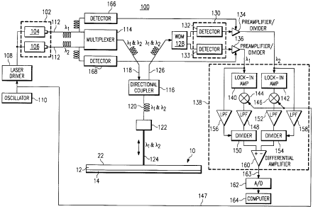
FIGURE 4 depicts a schematic diagram of temperature
sensor 100 which is an embodiment of the present
invention. Sensor 100 includes an optical energy source
or laser source 102 which includes first laser 104 and
second laser 106. Laser source 102 receives power from
laser driver 108, which in turn receives modulation
signals from oscillator 110. Oscillator 110 could in
turn be controlled by process control computer 70 of
FIGURE 3.
In one embodiment of sensor 100, the wavelengths of
laser 104 and laser 106 have been selected to be 850 nm
and 820 nm, respectively, for silicon wafer temperature
measurements. Other combinations of laser 104 at a
wavelength .l of 820 nm and laser 106 at a wavelength ~
of 810 nm, or laser 104 at a wavelength I of 810 n.m and
laser 106 at 780 nm can also be used for silicon wafer
temperature measurements. Laser source 102 is coupled by
a pair of optical fibers 112 to multiplexer 114.
Multiplexer 114 combines the laser beams it receives into
a single composite beam and is coupled to directional
coupler 116 by fiber-optic cable 118. In an alternate
embodiment, multiplexer 114 is an optical fiber bundle.
Directional coupler 116 is coupled through fiber-optic
cable 120 to fiber termination and collimating lens 122.
It is noted that directional coupler 116 can be replaced
with a fiber bundle without departing from the inventive
concepts of the present invention.
Lens 122 directs laser beam 124, which is a combined
laser beam from first laser 104 and second laser 106, to
TI-15257 2136SR6 PATENT APPLICATION
(32350-762)
and from wafer 10. Wafer 10 is positioned in apparatus
100 such that the rough backside surface 22 of wafer 10
is facing lens 122, and the frontside surface of wafer
10, which may simultaneously be under a fabrication
5 process, is facing away from lens 122.
Directional coupler 116 is coupled by fiber-optic
cable 126 to wavelength division demultiplexer (WDM) 128.
WDM 128 is coupled to detector module 130. Detector
module 130 comprises first detector 132 and second
10 detector 133 which may be low noise sensitive detectors.
Germanium, silicon, or avalanche photodetectors also can
be successfully used in detector module 130. First
detector 132 is coupled to first pre-amplifier/divider
134, and second detector 133 is coupled to second pre-
15 amplifier/divider 136. The outputs of pre-
amplifiers/dividers 134 and 136 are fed to signal
processor 138.
Signal processor 138 may have many analog, digital,
or hybrid embodiments, and it is not intended that signal
20 processor 138 be limited to the design shown in FIGURE 4.
In fact, signal processor 138 may be designed to include
laser driver 108, oscillator 110, detector module 130,
preamplifiers/dividers 134 and 136, and detectors 166 and
168. signal processor 138 includes lock-in amplifier 140
coupled to second pre-amplifier/divider 136, and lock-in
amplifier 142 that is coupled to first pre-
amplifier/divider 134. Signal processor 138 also
includes first mixer 144 coupled to lock-in amplifier
140, and second mixer 146 coupled to lock-in amplifier
142. These mixers multiply the outputs of their
respective lock-in amplifiers by a fraction of the laser
modulation oscillator signal from oscillator 110 supplied
on line 147.
TI-15257 PATENT APPLICATION
(32350-762)
21
Signal processor 138 also includes low-pass filters,
including low-pass filter 148 coupled to first mixer 144
and to first divider 150. Low-pass filter 152 is coupled
to second mixer 146 and second divider 154. Low-pass
filter 156 is coupled between pre-amplifier/divider 136
and first divider 150, and low-pass filter 158 is coupled
between first pre-amplifier/divider 134 and second
divider 154. The outputs of dividers 150 and 154 are
coupled to differential amplifier 160 which provides the
output of signal processor 138.
The output of signal processor 138 is coupled to
analog to digital converter 162, which is in turn coupled
to computer 164. In an alternate embodiment computer 164
may be embodied in process control computer 70 of FIGURE
3.
Output signal 163 of signal processor 138
corresponds to:
LRldl~lx.a - lR 'dll 1of Equations 10 and 13. Computer 164 extracts the
temperature of wafer 10 based on measurements at a
reference (e.g., room) temperature and at any unknown
temperature.
FIGURE 5 is representative of functional steps
executed by sensor 100 of FIGURE 4 of the present
invention in real-time non-contact measurements of the
temperature of wafer 10. The process is started at step
200 while the temperature of wafer 10 is known, typically
at a known reference temperature such as room temperature
(300 K). To first measure the rms surface roughness ro
of wafer 10, at step 204 oscillator 110 provides the
modulation signals for laser driver 108 to laser source
213~~86
TI-15257 PATENT APPLICATION
~ (32350-762)
22
102. At step 206, laser driver 108 provides modulated
electrical currents to laser source 102. Within laser
source 102, first laser 104 and second laser 106 provide
by way of fiber-optic cables 112 first and second laser
beams to multiplexer or combiner 114. At step 208,
multiplexer 114 combines the two laser beams into a
single beam. In step 210, the combined laser beams are
directed to and from wafer 10. This is accomplished by
multiplexer 114 providing combined beam 124 on fiber-
optic cable 118 to directional coupler 116. Directional
coupler 116 or fiber bundle controls the direction of
signals traveling on fiber-optic cable 120 between
directional coupler 116 and collimating/collecting lens
122. Directional coupler 116 allows the laser beams from
multiplexer 114 to travel on fiber-optic cable 120 to
lens 122. Lens 122 projects by collimation or focusing
multiplexed first and second laser beams 124 to backside
surface 22 of wafer 10 and also receives the specular
reflected beam.
In order to calculate the backside roughness ro at
the known reference temperature or room temperature with
Equation 11, it is necessary to measure the change in
specular reflectance R of wafer 10 backside surface 22
due to a change in wavelength I around the center
wavelengths of two laser beams directed to wafer 10.
This is accomplished by modulating the wavelengths I of
the two laser beams in composite beam 124 at step 206.
The change in specular reflectance values are determined
by measuring the change in specular reflected power P8p
values when the laser wavelengths of beam 124 are
modulated at step 206 and separated at step 216. The
reflected specular power P8P values provide the scattering
parameter values, which in turn, can be used to calculate
n
TI-15257 1v 6R r PATENT APPLICATION
(32350-762)
23
the backside surface roughness of wafer 10 at room
temperature.
The reflected specular power laser beam 124 is
collated by lens 122 and transferred by fiber-optic cable
120 to directional coupler 116. On the return path,
directional coupler 116 (or fiber bundle) directs the
reflected specular laser beam via fiber-optic cable 126
to WDM 128. At step 216, WDM 128 demultiplexes composite
beam 124 into reflected specular beams consisting of a
specular first laser beam and a specular second laser
beam, and provides signals representative of the
demultiplexed or separated beams to detector module 130.
At step 218 the extraction of the necessary data to
determine the rms surface roughness ro begins. In
detector module 130, first detector 132 and second
detector 133 measure the power of the reflected laser
beams for processing within signal processor 138. Pre-
amplifiers/dividers 134 and 136 condition the signals
from detectors 132 and 133, respectively, for processing
within signal processor 138.
In step 218, signal processor 138 extracts the
necessary information from the signals representative of
the specular reflected beams so that the change in
reflectance R due to a change in wavelength .t of the
beams can be identified. At step 219 a query is made as
to whether the temperature T of wafer 10 is known.
Assuming that the wafer is at a known temperature such as
room temperature, the flow proceeds to step 220. In step
220, applying Equation 11, computer 164 can calculate the
rms surface roughness ro of backside surface 22 of wafer
10. Once the rms surface roughness ro is determined the
flow returns to step 204 for continuous real-time wafer
temperature measurements.
2UPR6
TI-15257 PATENT APPLICATION
(32350-762)
24
To determine the unknown temperature of wafer 10 at
a later time, the process steps described for FIGURE 5
are repeated with the exception that at step 219, where
the temperature T of water 10 is unknown, the flow
proceeds to step 222. The changes in reflectance R due
to wavelength A modulation of the lasers are measured by
executing steps 204 through 218 of FIGURE 5, and by
knowing the value of the rms surface roughness ro at room
temperature, the unknown temperature T can be obtained in
real-time with Equation 13 at step 222.
For enhanced signal-to-noise performance in sensor
100 of FIGURE 4, cooling detector module 130 has been
found to be effective. For example, using thermoelectric
cooling, and operating detector module at temperatures
below room temperature reduces noise problems in sensor
100. Also, the wavelengths from laser source 102 can be
optimized by cooling laser source 102. This provides
enhanced signal-to-noise ratio and temperature
measurement accuracy in sensor 100.
When measuring the changes in specular reflectance
due to the changes in wavelengths, modulation of the
laser beams is employed. This can be accomplished by
using a square wave or a triangular wave from oscillator
110 to laser driver 108. Additional detectors 166 and
168 as shown in FIGURE 4 can be used to measure the
incident laser beam power levels. Detectors 166 and 168
provide signals that are proportional to the incident
beam power levels. By dividing the outputs of detectors
132 and 133 by the outputs of detectors 166 and 168,
respectively, the effects of laser power drifts and noise
can be cancelled out. The results of the division are
fed to signal processor 138 via preamplifiers/ dividers
134 and 136. This allows for significant enhancement of
TI-15257 PATENT APPLICATION
- (32350-762)
the signal-to-noise ratio and measurement repeatability
of system 100.
Laser current and wavelength modulations can also be
accomplished by using sinusoidal signals from oscillator
5 110 instead of triangular or square wave modulations.
Laser source 102 can be kept at a constant temperature to
eliminate any temperature related drifts. Moreover, if
all four detectors 132, 133, 166, and 168 are cooled to a
temperature between 200 K and 300 K, this minimizes low
10 noise effects and maximizes measurement resolution and
repeatability. It is also possible to use interferometry
to determine the precise change in wavelength I in each
laser beam due to modulation.
FIGURE 6 is a schematic drawing illustrating a
15 preferred embodiment of the temperature sensor of the
present invention showing the sensor's integration into
the rapid thermal processing chamber 30 of FIGURE 3. In
this figure, semiconductor wafer 10 is placed face down
with backside 22 facing the temperature sensors. FIGURE
20 6 includes three wafer temperature sensors 100 arranged
to provide multipoint temperature measurements on wafer
10. There is no limitation on the number of sensor
probes used for temperature profile measurements on a
wafer. Fiber termination and collimating lens 122 of
25 each temperature sensor 100 is shown secured in hollow
light pipes located within heatinq lamp module 54.
FIGURE 6 shows wafer 10 positioned below optical quartz
window 52. Optical window 52 not only serves to transfer
lamp optical flux and sensor laser beams to wafer 10, but
also maintains a controlled process environment within
the process chamber for processing semiconductor wafer
10. optical window 52 is optically transparent for both
lamp energy from lamp module 54 and the incident coherent
laser beams 124 transmitted and received by each
TI-15257 2130886 PATENT APPLICATIO:I
(32350-762)
26
temperature sensor 100. Optical transparency is a
function of the window material and the wavelength of the
optical energy passing through optical window 52, so the
material for window 52 is selected with optical
transparency in the desired band as an essential feature.
For, example, for 1.3 um laser beams, a window material
such as quartz can be used. Wavelengths larger than 4 nm
will require alternative window materials, such as
sapphire.
The operation of the multipoint temperature sensors
of FIGURE 6 is as described for the operation of
temperature sensor 100 of FIGURE 4. Each temperature
sensor 100 causes laser beam 124 to be transmitted by
lens 122 through quartz window 52 and through wafer
backside ambient 170. Each laser beam 124 strikes wafer
10 backside and a portion of the reflected beam is
transmitted as a specular beam back to lens 122, and the
remaining portion is scatter reflected. To measure the
change in specular reflectance of wafer 10 backside due
to laser wavelength modulation, each laser beam is
modulated and its effects are measured. Using the
measured change in specular reflectance values, and
measured room-temperature rms surface roughness ro for
wafer 10, the temperature of wafer 10 is calculated in
real-time for the wafer positions corresponding to the
sensor probe locations.
It is noted that by including multiple temperature
sensors 100 within RTP reactor 30, it is possible to
measure a temperature map or profile for wafer 10. The
measured temperature values by each system 100 can be fed
into a multi-zone temperature control system for
establishing uniform and repeatable processing. It
should also be noted that each lens 122 of the
temperature sensors shown in FIGURE 5 can be coupled to a
TI-15257 2 136Q ?! ~ PATENT APPLICATION
' (32350-762)
27
fiber bundle. A fiber bundle can be used to transmit the
laser beam (with two multiplexed wavelengths) and to
receive a specular reflected beam in each sensor probe.
FIGURE 7 shows an alternate embodiment of the
present invention based on the use of mirrors and
splitters instead of fibers. In addition to those
similar components of temperature sensor 100 of FIGURE 4,
the wafer temperature measuring sensor 180 of FIGURE 7
includes beam splitters 182, 184, 192, and 194. First
laser 104 directs a first beam at splitter 192 which
splits the first laser beam directing a portion onto
detector 196 and the remainder of first laser beam to
beam splitter 182. Beam splitter 182 then sends a
fraction of the beam to beam splitter 184 which in turn
sends a fraction of the beam originated from first laser
104 to wafer 10. Second laser 106 directs a second laser
beam to splitter 194 which splits second laser beam into
two portions. The first portion travels to detector 198
and the remainder to beam splitter 184. Beam splitter
184 combines a fraction of the laser beam from laser
source 106 with a fraction of the beam from first laser
source 104 and sends the combined beam to wafer backside
22.
The combined portions of laser 104 and 106 beams
form combined beam 124 which is directed towards wafer 10
and its specular reflected portion is guided by beam
splitters 182 and 184 towards prism demultiplexer 190.
Prism demultiplexer 190 performs wavelength division
demultiplexing on the specular reflected combined laser
beams and provides the separated reflected first and
second beams to detector module 130. The output signals
of detector module 130 are provided to signal processor
138 (not explicitly shown in FIGURE 3) for processing as
TI-15257 3 f;, Q
R6 PATENT APPLICATION
(32350-762) V
28
described in connection with the discussions for
FIGURE 4.
The lasers of laser source 102 depicted in FIGURE 7
can be tunable diode lasers. Tunable diode lasers can be
modulated by modulating their drive current with laser
driver 108 and oscillator 110. Current modulation varies
the laser output wavelengths and the intensities of the
laser beams from laser source 102, resulting in
simultaneous amplitude and frequency modulation. In an
ideal system only modulation of the laser wavelengths by
modulating their intensity levels would occur. However,
this may not be possible. Therefore, beam splitters 192
and 194, and detectors 196 and 198 are used to monitor
the intensities of the incident laser beams from lasers
104 and 106. The output signals from detectors 132 and
133 are then divided by the output signals from detectors
196 and 198, respectively, in order to cancel intensity
variation effects.
Black body absorbers 186 and 188 dissipate the
excess laser beam powers exiting beam splitters 182 and
184 in the directions of the original incident beams.
In either embodiment of wafer temperature measuring
apparatus shown in FIGUREs 4 or 7, a single laser can be
employed rather than the two shown. The single laser
embodiment also has capability for direct measurement of
the surface roughness and calculation of wafer
temperature. The one laser apparatus must provide real-
time measurement of both the specular as well as
scattered reflected beams off of the wafer surface.
It is also noted, that while the several embodiments
of the present invention have been discussed in
connection with obtaining the rms surface roughness and
specular reflectance from backside surface 22 of wafer
10, the present invention can also be used to measure
(323505762) 2~~G~~~ PATENT APPLICATION
29
temperature T of wafer 10 by directing the laser beams to
the frontside surface of wafer 10. Measuring the change
in specular reflectance due to the change in wavelength
on the front side of wafer 10 can be accomplished with
the sensor of the present invention. Also, the several
embodiments of the present invention discussed herein can
also be used in applications other than semiconductor
processing. The sensor of the present invention is
effective in measuring the temperature of any workpiece.
Although the present invention has been described in
detail, it should be understood that various changes,
substitutions, and alterations can be made hereto without
departing from the spirit and scope of the invention as
described by the appended claims.