Note: Descriptions are shown in the official language in which they were submitted.
~3732i
--1--
METHOD FOR MANUFACI~URING A T~ ILM EAS MARKER
BACKGROUND
The present invention relates generally to thin-film ma~nP,tic devices. In
particular, the present invention is a method for m~nllf~lring thin-film m~gnP,tic
~"Lk~,~ ofthe type used in electronic article surveillance systems.
Magnetic-type e~ IOILC article surveillance (EAS) systems are co"""only used
to prevent the theft or other ~n~llthori7P~d removal of articles such as books and clothing
from libraries, bookstores and department stores. EAS systems of this type include
m~,~ which are affixed to the articles to be protected, and an interrogation system
inr~ ing detection panels positioned on opposite sides of a detection corridor leading to
exits of the b~ lin~ in which the articles are located. The interrogation systemproduces an alternating m~gnetic interrogation signal at a predetermined frequency
which is ll~n~.l.itled between the detection panels. The markers are relatively small
",~",~e,~ that include m~gnPtic material. Unless effectively disabl~' e.g., at a check-out
counter, the m~nPtic material in the marker emits h~rml~ -s of the predeterminedinterrogation frequency when exposed to the interrogation signal. The interrogation
system monitors the p-~sence of these harmonics, and generates an alarm signal when
2 0 the harmonics are detected Markers of this type that can be reversibly deactivated are
known as dual status markers. EAS systems of this type are described generally in the
Elder et al. U.S. Patent 3,665,449 and commercially available from Minneso~a Mining
and M~mlf~chlring Company (3M).
Markers used in EAS systems of this type typically include elongated strips
(e.g., 15.0 cm x 0.6 cm) of amorphous or polycrystalline ferromagnetic materialsexhibiting m~gnetic properties im~ ng those known as low coercivity and high
permeability. The Piotrowski et al. U.S. Patent 5,083,112 discloses a more comract
marker which incl~ldes a plurality of thin-film layers of permalloy, an alloy of nickel and
iron (NIFe). The thin-film NiFe layers are separated by nonm~gnPtic thin-film layers of
SiOX which allow magnetostatic coupling between the layers, but inhibit PY~.h~n~e
coupling that can in~ ase the coercivity of the marker. Conventional electron beam
7321
._~
--2--
(E-Beam) deposition processes are used to coat the thin-film layers of ma~netic material
on a flexible polymer substrate. The nonma~np~tic thin-film layers of SiOx are grown by
conventional sublim~ti~n deposition processes.
The thin-film layers of m~nP,tic material are coated onto the substrate in the
5 presence of a ma~netic field which causes the magn~P,tic film to form in such a manner
that a desired axis of m~çl;~ n known as the "easy" axis of m~el;~"l;on, is
developed in the film. When exposed to an alternating interrogation signal aligned with
the easy axis of ma~Pti7~tion, the m~gnetic states of the thin-film layers are relatively
easily driven to saturation, which induces the greatest ,espollse in the interrogation
10 signal. In other words, the marker can be easily m~eti7ed and will provide the
greatest lesponse in the interrogation signal when it is exposed to the interrogation
signal with the easy axis of m~ l;on aligned with the interrogation signal. In
contrast, when the interrogation signal is aligned with the "hard" axis of magnPti7~tiQn,
an axis generally perpen~ic~ r to the easy axis, the layers become m~ nPti7Pd to only a
15 relatively small value and induce little response to the interrogation signal.
The ability of m~gnp~tic-type EAS systems to detect marked articles is thereforedependent to some extent on the orientation of the markers as they are transported
through the detection panels. EAS systems typically include interrogation system s that
generate an interrogation signal along only one axis. Articles protected by systems of
2 0 these types will produce the greatest response and be most easily detected when the
marker ~tt~ched to the article has its easy axis of m~gneti7~tion oriented parallel to the
interrogation signal axis as it passes through the detection panels. The m~gnitude of the
induced response, and therefore the ability of the interrogation system to detect the
p.~ sence of marked articles, decleases with inc.t;asll~g angle between the marker's easy
25 axis of ma&n.,t;~ n and the axis ofthe interrogation signal. The interrogation system's
ability to detect the 1ll~ is lowest when the easy axis of m~p,~e~ ;on is oriented
pel~,e~.-l;c.~l~r to the axis ofthe interrogation signal.
The Piollow~ki et al. U.S. Patent discloses a dual axis or bi-directional m~ netic
marker which inrl~ldçs a plurality of m~netic thin-film NiFe layers sep~led by
30 nr)nma~Ptic thin-film SiOx layers. The dual-axis response is obtained by assembling
21373~.
two ma~nP,tic thin-films ofthe type de~-il,ed above so the easy axes of ~ et;~l;on of
the films are oriented at a perpPn~ or 90 angle with respect to one another. Dual
axis n~ke-s of this type offfer considerable advantages over single axis markers since
the interrogation system's ability to detect the ll,a.kel~ is less sensitive to the oriPnt~tion
5 ofthe marker as it is l~lspo~led through the detectio~ panels. Unfortunately, current
methndc of m~nllf~lring dual axis markers of this type are relatively c-:s,,,plic~led and
add to the cost of the --a~ . Because the easy axis of m~çl;~,.lic)n of the thin-film
fl~ lc aligns parallel to the axis of the magnetic field applied during deposition, the
dual axis n~ke,~ must be made either by l~ l;.,g together two or more thin-film
10 elPrnpntc so their easy axes of ma~Pti7~tinn are perpPn-~icul~r to one another, or
depositing the thin-film layers in a coating system capable of producing the orienting
magnetic fields in two perpen~liculq~ directions. Again, these techniques are relatively
complicated and add to the cost of the markers. There is, lLererore~ a cnntin-~ing need
for more efficient methods for m~nllf~ctllring dual axis m~gnetic thin-film markers.
SUMMARY
The present invention is an improved method for m~nuf~cturing a thin-film
ma~etic device having an easy axis of m~.eti~l;Qn which is perpendicular to the axis
of a ma~nP,tic field applied during the deposition. This invention is based on the
20 discovery and w-~e~;Led result that thin-film layers of m~gnP,tic m~teri~l grown or
deposited or a substrate in the presence of a m~gn~P.tic field can be produced with an easy
axis of m~ ..l;on which is perppndic~ r to the axis of the applied magnetic field if
the layers are relatively thin.
One embodiment ofthe invention incl~ldec providing a substrate having a surface
25 char~ctPri7ed by first and second generally perpen~icul~r axes. A m~etic field
oriçnted parallel to the first axis is applied to the surface of the substrate. A relatively
thin thin-film layer of magnetic m~tçri~l is grown on the substrate in the presence of the
ma~etic field. The relatively thin layer is grown to a thickness sufficiently thick for the
layer of material to exhibit m~gnetic p-upellies that are substantially independent of
3 0 surface effects, but sufficiently thin that the easy axis of m~ t;,~ll;on is oriented parallel
Z137321
to the second axis. In a p~ led embodiment, the method further int~ es grU~illg a
plurality ofthe relatively thin layers of magnPtic material on the substrate in the presellce
of the m~netic field, and growing a thin-film layer of nC)nmA~netic material between
each ofthe relatively thin layers of magnPtic material.
The invention can also be used to mAmlfA~Ire a dual-axis m~gnPtic marker of
the type used in electronic article surveillance systems. The method inc.l~ldP~s providing a
web of flexible substrate having a surface and characterized by generally p~ r
down-web and cross-web axes. Sources of m~gnetic and nonm~gnetic material are
provided at a deposition station. A magnet for applying a ma~nPtic field oriented
parallel to the cross-web axis of the substrate at the deposition station is also provided.
The web is driven in a direction parallel to the down-web axis in alternating forward and
reverse passes through the deposition station. A down-web aligned thin-film layer of
ma~ne.tic material is deposited on the substrate in the p,t;sence of the ma~Ptic field
during each of a plurality of down-web aligned stack-forming forward and reversepasses through the deposition station. Each down-web aligned layer is deposited to a
thickness s ffici~Pntly thick that the layer exhibits m~Ptic properties that are
s Ib~n~l1;Ally independent of surface effects, yet s ffici~ntly thin that the easy axis of
m~e~ ;on of the material is oriented parallel to the down-web axis. A thin-film layer
of nol....~elic material is deposited between each down-web aligned layer during each
2 0 of the plurality of down-web aligned stack-forming forward and reverse passes through
the deposition station. A down-web aligned stack of relatively thin thin-film layers of
ma~nPtic material separated by layers of nnnma~nPtic material and having an easy axis
of m~.P,~ l;t)n oriented parallel to the down-web axis is thereby formed. A cross-web
aligned thin-film layer of mAgnPtic material is deposited on the substrate in the presence
25 of the magnPtic field during each of a plurality of cross-web aligned stack-forming
forward and reverse passes through the deposition chamber. Each cross-web aligned
layer is deposited to a thickness sufficiently thick that the easy axis of the mAEneti7~tion
of the material is oriented parallel to the cross-web axis. A thin-film layer ofnonm~gnPtic material is deposited between each cross-web aligned layer during each of
3 0 the plurality of cross-web aligned stack-forming forward and reverse passes through the
- 2~37~2~.
-
--5--
deposition station. A cross-web aligned stack of relatively thick thin-film layers of
maen.otic material ~ ed by layers of n-)nm~etic material and having an easy axisof ...a~ ion oriented parallel to the cross-web axis is thereby formed. Magneticmarker sectionQ are then separated from the web.
BRIEF DESCRIPTION OF THE DRAWINGS
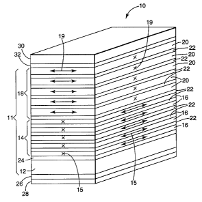
Figure 1 is a perspective view (not to scale) of a l~m;n~ted dual axis m~netic
thin-film EAS marker m~nllf~ red in accordal1ce with the present invention.
Figure 2 is a side view of a coating system which can be used to m~mlfi~chlre
ma~tic thin-film devices in accordance with the present invention.
Figure 3 is a graph of the measured B-H hysteresis loops about cross-web and
down-web axes of a sample thin-film m~etic device m~n~lf~ctllred in accordance with
the present invention.
Figure 4 is a graph of the measured coerciw force along the cross-web axis at
twelve spaced loc~tion~ across the width of each of six samples from an ~long~ted web
of a thin-film m~gnetic device m~n~lf~ctured in accordance with the present invention.
Figure 5 is a graph of the measured coercive force along the down-web axis at
twelve spaced locations across the width of each of six samples from an elongated web
of a thin-film m~etic device m~nllf~ct~lred in accordance with the present invention.
Figure 6 is a graph of the measured 15th harmonic signal generated by
prototype ma~netic devices m~mlf~lred in accordal1ce with the present invention
when ~ osed to an interrogation signal oriented along the down-web and cross-webaxes.
Figure 7 is a graph of the measured B-H hysteresis loops along cross-web and
2 5 down-web axes of a sample thin-film m~gn.o,tic device m~nllf~ct~lred in ac cordance with
the present invention and inclllrli~ only a down-web aligned stack of relatively thin thin-
film layers.
Z13'7~
DETAILED DESCRIPTION OF THE PREFERRED EMBODIMENTS
The present invention is based on the u n~,.pe ,~ed discovery that thin-film layers
of ma~P.tic material grown or deposited on a substrate in the p~esence of a m~ P.tic
field can be produced with an easy axis of m~ l;on which is pelye~ r to the
5 axis of the applied ma~nPtic field if the thin-film layers are relatively thin. For purposes
of the present spe~ific~tion, the term "relatively thin" is defined to refer to a thin-film
sllffic;Pntly thin such that the easy axis of m~ ;on aligns p~ll.æ~dicul~r to the axis
of the applied ma~netic field. As described below, for eY~nnr'e, NlFe layers grown by
elc~r~,n beam evaporation to a thickness of about 200 ang~,ol--s in the presel~ce of a
250-300 oersted (Oe) m~gnetic field have exhibited this characteristic. This Illlc'-ness
co"")d.es to thickness values greater than about 300 angstroms to which the NiFe thin-
film layers are typically deposited to obtain an easy axis of magnetization which is
aligned parallel to the axis of the applied m~gnPtic field. ~lthough specific e~l~p!e3 for
NFe thin-films are described, each thin-film material will have di~ere"l l' ~l nPeees at
15 which it is sllffi~;Pntly thin such that its easy axis is aligned perp-Pndic~ r to the axis of
the applied ma~nPtic field. Any thin-film m~tçri~l and thickness thereof which satisfy the
present "relatively thin" shall therefor be understood to fall within the spirit and scope of
the present invention.
This discovery can be used to greatly increase the efficiency of thin-film
2 0 ma~P,tic device m~mlf~ctllring processes since thin-films ofthis type having an easy axis
of ma~ ;on along either of two perpçntliclll~r axes can be produced with
eqllirmpnt configured to apply a m~gnPtic field along only one ofthe axes.
A dual axis, nonline~r response, thin-film m~gnetic electronic article surveillance
(EAS) marker 10 m~nllf~ctllred in accordance with the present invention is illustrated
25 generally in Figure l. Marker l0 incl~ldçs a l~min~ted thin-film m~etic device ll
which incl~ld~Pe a substrate 12 which supports a down-web aligned (i.e., a second axis
aligned) stack 14 of relatively thin thin-film layers 16 of m~gnetic material, and a cross-
web aligned (i.e., a first axis aligned) stack 18 of relatively thick thin-film layers 20 of
ma~P,tic material. Each relatively thin layer 16 and relatively thick layer 20 are
3 0 separated by a thin-film layer 22 of non~ etic material. In the embodiment shown, an
23L3~
--7--
optional adhesion-promoting primer layer 24 overlays substrate 12 below down-webaligned stack 14. A pressure sensitive adhesive layer 26 overlays the surface ofsubstrate 12 opposile stacks 14 and 16, and is used to securely mount marker 10 to a
book or other article under surveillance. A release liner 28 protects the adhesive layer
5 26 until the marker is to be attarhf~d to an article to be protected. A protective layer 30
is secured to the upper surface of cross-web aligned stack 18 by pressure sensitive
adhesive layer 32. Plole~ e layer 30 can indude a printable surface.
Substrate 12 is a thin and flexible polymeric .,leml)er capable of with~t~n~i~ the
high te""~)el~t~lres present during the deposition of layers 16, 20 and 22. In one
10 p,~l~;d embodiment, substrate 12, is an ICI Melinex thermally stabilized PET
(polyethyleneterephll,alate) material having a thickness of 50 llm. Other polymers such
as polyimide can also be used for substrate 12, as can thin metallic foils of nonm~etic
c~.~ steel, ~ minllm or copper. An oxygen glow discharge can be used to form thea~lh~Q;on-promoting primer layer 24. Polymeric substrates 12 ranging between 12 and
1 5 75 llm thick are typically used for markers 10.
Thin-film layers 16 and 20 are formed from m~gnetic~lly soft materials
characterized by low coercivity and high p~;",-eabil;ly. Materials with these
characteristics are capable of producing the desired nonlinear m~gnetic response when
exposed to an alte",alii-g interrogation signal. Prototypes nl~kel~ 10 were produced
2 0 with crystalline permalloy-type NiFe alloys. In one embodiment, the nominal
composition of layers 16 and 20 is 81.5 weight % Ni and 18.5 weight % Fe. Other
amorphous, polycrystalline, or crystalline ferrom~gnetic materials having these
properties can also be used for layers 16 and 20.
As described below, thin-film layers 16 and 20 are deposited in the presence of
25 an orienting m~gnetic field so these layers in stacks 14 and 18, respectively, have easy
axes of ...A~-el;~ nn which are pel~ r to one another. In Figure 1, for ~x~r"~,le,
the easy axis of m~-eli~lion of layers 16 in down-web aligned stack 14 are oriented
parallel to a first or down-web axis ,el),esenled by the "x"s and arrows 15. In this
c~mple, the easy axis of m~gneti7~tion of layers 20 in cross-web aligned stack 18 are
30 oriented parallel to a second or cross-web axis ,t;plese"led by the "x"s and arrows 19.
213~
--8--
Nonm~g,nP,tic layers 22 can be formed from oxides of silicon or ~lllminllm or
other m~teri~ls SiOx was used as the material for layers 22 of prototype ,..~I~e~ 10,
where 'x' is app~ n~ y 1.
An ~o ~ Y thin-film coating system 40 which can be used to deposit
magnetic thin-film layers 16 and 20 and nonmagnf,tic thin-film layers 22 onto substrate
12 can be described with lerelence to Figure 2. It shall be understood that each...a~nf.~ic and non-m~enetic thin film layer will herein be described as deposited on the
substrate even though there may be one or more intervening layers of m~gnetic or non-
,..agn.,l;c material between the thin-film layer and the polymeric substrate 12. Coating
1 0 system 40 incl~de~ a rotating heated drum 42 and a web drive system incllldin~ a pair of
take-up spools 44A and 44B, all of which are enclosed in a vacuum çh~mh~r 46. An~lohg,~1ed web 45 of substrate 12 is driven be~ween take-up spools 44A and 44B in
alLel-.aling forward and reverse passes through a felloln~enstic material deposition
station 48. Web 45 is biased into ene~e~omçnt with drum 42 at deposition station 48 by
rollers 50. Nonm~enetic material sources 56A and 56B are positioned below web 45belweell deposition station 48 and take-up spools 44A and 44B, respectively.
Conventional vacuum systems (not shown) are used to evacuate cl~-lbel 46. Although
not shown in Figure 2, take-up spools 44A and 44B and nonm~etic material sources56A and 56B can be po~itioned in separate vacuum chambers. In one embodiment the2 0 vacuum system incl~ldes a col"l)inalion of turbomolecular and cryogenic pumps capable
of evacu~ting chamber 46 to a base pressure of at least SxlO~ Torr. Coating system 40
is IllA; li~ ed at a pressure of about lxlO-5 Torr during the coating m~mlf~ct~lring steps
described below.
A ~elmholt7 coil 52 incl~l~lin~ a coil 54 on each side of web 45 (only one coil 54
2 5 is visible in Figure 2) is also mounted within vacuum ch~nber 46. H~lmholt7. coil 52
generates an orienting m~ netic field which is perpsndic~ r to the longitu(lin~l axis of
the web 45 and parallel to the rotational axis of drum 42, i.e., is oriented in a "cross
web" or "first web axis" direction. Helmholtz coil 52 is confi~lred to generate an
orienting ma~,tic field having a relatively con.~ ma~nit~lde across the width of the
web 45. Coil 52 is positioned to locate the center of the orienting field at the
2~37321
g
i"lel~lion of drum 42 and web 45 in deposition station 48. The strength of the field
gen~"aled by ~PImholt7. coil S2 is pref~l~bly sllffic;~nt to .~ el;~ y saturate and
produce a high degree of anisoll~y in the m~netic properties ofthe thin-film layers 16
and 20 being grown. Field ~lle~ ls of 8,000 - 16,000 A/m (1 Oe = 80 A/m) are
generally sl~ffic;ent for this purpose.
One or more electron beam evaporation systems 58 are mounted below web 45
at deposition station 48. Exe~ y coating system 40 used to produce prototype
magll~tic devices 11 is configured to coat sixteen inch (40.6 cm) wide webs 45 of
substrate 12, and includes two evaporation systems 58 (only one of which is visible in
1 0 Figure 2), each of which is positioned applo~s"~alely four inches (10.2 cm) from the
opposite edges of the web along the cross web axis. Each electron bearn evaporation
system 58 may include, for e,.~p!e, a three inch Edwards Temescal electron beam gun
and a Temescal wire feed apparatus. The wire feed apparatus enables lengthy
depositions with good compositional control. The power applied to the electron beam
1 5 guns was varied to give the desired film deposition rates. Shutters and baffles (not
shown) are also used in a conventional manner to obtain nearly normal inf ;d~nce of the
e~dpo.~,l onto the web 45.
In the prototype coating system 40 described above, sources 56A and 56B
include a crucible and inductive heater (not separately shown in Figure 2) for depositing
layers 22 of SiOx by a sublimation process. Colll,-,elcially available silicon monoxide
chips of app,ox;.n~PIy 6mm in size can be used as the raw material. Sources 56A and
56B can be operated in a method similar to that described by Maisel and Glang inHan~book of Thin Film Technology, McGraw Hill, New York 1970, to thermally
deposit the SiOx layers 22. The deposition rate is controlled by adjusting the
2 5 te"-pe ~lures ofthe deposition crucibles.
Coating system 40 is operated by driving the elongated web 45 of substrate 12
between take-up spools 44A and 44B in alternating forward and reverse passes through
deposition station 48. During each pass, evaporation systems 58 and the nonma~netic
m~tPri~l sources 56A and 56B are operated to deposit half of a nonm~Ptic thin-film
3 0 layer 22, one ma~etic thin-film layer 16 or 20, and half of a subsequent nonmagnP.tic
2137321
i~
thin-film layer 22, sequPntiAlly~ on the lower side of the web. For c ,- le, during a one
forward pass, web 45 is unwound from take-up spool 44A and wound onto spool 44B.Evaporation systems 58 and nonmagnP,tic material sources 56A and 56B are operated to
deposit the second half of a first nonm~gnP,tic thin-film layer 22, a first ~ r1;c thin-
5 film layer 16 and the first half of a second nonm~eneSic thin-film layer 22, re~,e~;~h~ely,
on the surface of the web during this pass. A reverse pass follows imme~ tPly
afterward, with the web 45 being unwound from spool 44B and rewound onto spool
44A Evaporation systems 58 and nonma~nP,tic material sources 56B and 56A are
operated to deposit a second halfofthe second nonmAgnP.tic thin-film layer 22, a second
1 0 layer 16 and a first half of a third layer 22, respectively, on the layers deposited during
the pleced,ng pass. This procedure is repeated as often as required to produce the
Ag~ ;c device 11 having a down-web aligned stack 14 and a cross-web aligned stack
18 inclllriine the desired number of relatively thin and relatively thick layers 16 and 20,
ely.
Plololy~e thin-film m~etic devices 11 were fabricated from a sixteen inch
(40.6 cm) wide web 45 of Melinex thermally st~hili7ed PET substrate 12. The web 45
was driven at a speed of about forty feet per minute (101.6 cm/min) with drum 42heated to a tel"pe,~ re of about 80C. Before depositing the first thin-film layer 16 or
20, the web 45 is deg~csed by driving the web through several passes near IR lamps (not
2 0 shown) to remove any water adsorbed by the web. Other outg~c.~ing procedures, such
as heating drum to about 300C and driving the web through several passes over the
drum can also be used, depending on the properties of the substrate employed. It has
been found that pre-heating of the web before the first pass with IR lamps and heated
drum tends to inhibit cracking of the films. An orienting magnetic field of about 250-
2 5 300 oersteds was provided by Helmholtz coil 52. In addition to aligning the easy axes
of m~gnP,tic layers 16 and 20 during deposition, the magnetic field produced by coil 52
helps position the electron beams produced by evaporation systems 58 to ensure that the
beams properly impinge on the crucibles in the evaporation systems. No primer layer 24
was deposited on the prototype m~etic devices 11.
21 ~7;~21.
Relatively thin NlFe thin-film layers 16 of stack 14 which are grown in the
manner and under the conditions described above to thi( ~neccPs in the range of 125-225
an~ ul,ls have easy axes of ~ e~ on which are parallel to the down-web axis.
This easy axis orientation is pel~el-~l;cul~r to the cross-web axis of the orienting
5 ma~n~P,tic field applied during the growth of relatively thin thin-film layers 16. As the
thickness of relatively thin thin-filrn layers 16 is decreased below 175 al1g~llù"-s, surface
effects exert increasing control over the ma~etic characteristics of the layers and result
in less de~. ~le ma~nPtic properties, incl~ ing higher values of coercivity. As relatively
thin NlFe layers 16 are grown to th c~nPccP~s beyond 225 angstroms, the extent to which
10 the easy axis of ma~nPti7~ti~ln of these layers is aligned with the down-web axis
decreases. At l} -~nPcces of about 300 or more angstroms, the easy axis of
m~e~ ion is substantially aligned with the cross-web axis of the orienting m~etic
field.
Relatively thick thin-film layers 20 of stack 18 are thelefore grown to a
lhic~ness of at least about 300 angstroms. The coercivity of relatively thick layers 20
incleases with increasing thiG~necc of the layers and effectively places limits on the
thickness of the relatively thick layers. The th -~nPsces to which relatively thick and
relatively thin layers 16 and 20 can be grown, yet still exhibit the desirable properties
described herein, can vary and will depend on factors such as the nature and
composition ofthe m~gn~Ptic materials, the growth process p~ tel~ such as speed
and telllpel~ re, and the strength of the orienting magnP.ti~ field applied during the
coating process.
Following the growth of stacks 14 and 18 on web 45, the thin-film ma~netic
device 11 is removed from coating system 40. Sheets of adhesive layer 26 and release
Liner 28 are appLied to the side of substrate 12 opposite stacks 14 and 18. In a similar
manner, an adhesive layer 32 and protective layer 30 can be secured to the upper surface
of stack 18 to co rl le a roll of marker stock. Individual markers 10 can then be cut,
slit or otherwise separated from the roll of stock.
One embodiment of a thin-film m~etic device 11 was fabricated in the manner
3 0 des.ilil,ed above with a down-web aligned stack 14 having six about 200 angstrom thick
2~ 373;21.
--1 2--
relatively thin NlFe layers 16, and a cross-web aligned stack 18 having five about 350
angstrom thick relatively thick NlFe layers 20. A SiOx layer 22 having a thic~nes~ of
about 125 ang~l,o-l,s sepal~les each thin-film layer 16 and 20 in this device 11. One
inch square (2.54 cm2) samples of these devices 11 exhibit a down-web easy axis of
5 m~gn~ ;on, which is believed to originate from crystaUographic or crystallite
olielltalions within the relatively thin layers 16 of down-web aligned stack 14, even
though these thin-film layers were deposited in the pr~sence of the 250-300 oersted
cross-web ..~)el;c field. The easy axis of the relatively thick layers 20 of cross-web
aligned stack 18 is oriented in the cross-web direction as c,~pe~iled. Markers 10
10 m~mlf~lred from this m~gnetic device 11 will thelerole exhibit dual-axis magnetic
characteristics. The number of thin-film magnetic layers in each stack 14 and 18, and
the order in which these stacks are deposited on the substrate 12, can also be varied to
meet specific requi,elllell~s of the applications in which the film is to be used. For
eA rlC, the interrogation signal es~onse strength will be greater if the number of thin-
15 film ...~-el;c m~teri~l layers is incleased, but the cost of m~nllf~lring will also be
greater. Figure 3 is a graph of the measured B-H hysteresis curves from the sample
described above along both the down-web axis (shown by a broken line) and the
cross-web axis (shown by a solid line).
Meas~remellLs have shown that the coercive force, measured with m~gnetic
2 0 fields applied along both the down-web and cross-web axes are relatively co~ l over
a region of at least six to seven inches (15.2-17.8 cm) in the center of the sixteen inch
web 45 from which the sample described above was taken. Figure 4 is a graph of the
cross -web coercivity (Hc) measured at twelve locations across the width of the web.
Curves A-F were obtained at six down-web spaced positions on the web 45. The six2 5 samples A-F were made during difl`erenl depositions over a period of about one week.
Similarly, Figure 5 is a graph of coercive force (Hc) along the down-web axis from the
same s- ~'es The measul~"le"l~ illustrated in Figures 4 and 5 were made on one inch
square samples using an 18 K~, 1.5 oersted applied m~gnetic field. The fact thatsample A in Figures 4 and 5 deviates somewhat from the rem~in(ler of the samples can
3 0 be ~ d by the fact that it was from the first deposition after pumpdown of the web
21373~21.
--13--
45 on which the deposition process started, and likely had residual water vapor that had
not been driven out by the oul~ c~ P~ procedures. This ph~l~o.~.~non is com",ollly
observed.
Meas~re",e"ls have also shown that the m~gnihld-p~s of the responses produced
5 in interrogation signals exposed to these six samples are relatively con~ along both
the down-web and cross-web axes for samples taken from a region within six to seven
inches ofthe center of web 45. Figure 6 is a graph ofthe 15th h~l~lolLc signal re~.ollse
generated in an 18 KHz, 1.5 Oe interrogation signal exposed to these samples when
oriented along the down-web and cross-web axes of the s~llp!cs Each data point in
10 Figure 6 is an average of the six samples A-F at the given sample positions.
Figure 7 is a graph of the B-H curve along both the down-web axis (shown by a
solid line) and cross-web axis (shown by a broken line) of a sample of a thin-film
m~gmPtic device inrlll-iing siX 200 angstrom thick thin-film layers 16 of NiFe separated
by 125 ang~lrom thick layers 22 of SiOx. The sample from which the measurements
15 shown in Figure 7 were taken was grown in the manner described above on a PETsubstrate 12, but had no relatively thick thin-film layers 20. The highly anisolropic
properties of this sample, and its down-web easy axis of magnPti7~tion (even though
grown in a 250-300 Oe cross-web magnPtir field) are evident from this Figure.
The thin-film m~gnPtir device and EAS marker m~nllf~ lring method described
20 above offers considerable advantages over those of the prior art. In particular, the
method enables the fabrication of a nonlinear, dual-axis device and marker without the
need to l~min~e together two or more discreet films, or to rotate the m~gnPtic field
applied dunng film growth, to produce stacks of layers having perpendicul~r easy axes.
These devices can be produced with the relatively high permeability and low coercive
25 force necPs~ry to generate strong responses in the interrogating fields to which the
devices are exposed. High quality dual-axis magnetic thin-film devices and EAS
markers can lL~,~ro,~ be efficiently fabricated at lower cost.
Although the present invention has been described with ,~;r~,ellce to ,ol~"ed
embo-lirnPnt.~, those skilled in the art will recognize that changes may be made in forrn
3 0 and detail without departing from the spirit and scope of the invention. In particular,
2137321
-~4- -
although the prototypes described above were m~n~lf~ch~red with the down-web aligned
stack on the substrate below the cross-web aligned stack ma~etic devices in
acco.d~lce with the present invention could be fabricated with the stacks in the reverse
order. The orienting m~gnetic field could also be aligned with the down-web axis rather
5 than the cross web axis as described above. Furthermore, the present invention can also
be used to produce down-web aligned and cross-web aligned layers in a dual status
(reversibly deactivatable) thin-film ma~netic device.