Note: Descriptions are shown in the official language in which they were submitted.
W094/00868 ;~ ~ 8 7 4 7 I PCT/US93/06118
TRANSPORT SYSTEM FOR WAFER PROCESSING LINE
Field of the Invention
This invention relates to a transport sys~em
for a wafer processing line. More particularly, this
invention relates to a transport system which includes
one or more linear magnetic drive units for translating a
wafer carrier along a processing line.
Backqround of the Invention
Semiconductor wafer manufacture generally
requires the performance of a plurality of processing
steps according to a predetermined sequence under vacuum
conditions. In one type of wafer processing system,
evacuatable modules or housings connect serially, and
each housing serves as the site for performing one of the
processing steps, such as heating or sputter coating, or
lS simply to initially isolate wafers from the outside
environment. Wafer processing systems which utilize a
plurality of serially-connected housings are commonly
referred to as ~in-line~ processing systems. Generally,
~ =
:~13~?1
W094/00868 PCT/US93/06118
--2--
these "in-line~ systems allow ~Xi~ wafer throughput
per unit time.
For in-line wafer processing systems where
processes such as sputtering, vacuum evaporation, plasma
etching are performed, it is nec sc~ry to move some parts
such as substrates and shu~ters. Motion of these parts
in vacuum is usually accomplished by using vacuum
feedthroughs of various kinds. A feedthrough penetrates
the walls of the vacuum system to provide a physical
connection such as a shaft ~etween the atmospheric side
and the vacuum side. These feedthrough connections have
seals to prevent leaks from the atmosphere into the
vacuum.
Usually a rotary feedthrough is used to
transmit rotational motion into vacuum. Rotation is then
converted to linear motion by means of m~ch~nical
components such as a ball screw, rack and pinion, worm
gear, nuts, etc. which depend on friction to operate.
In many applications the cleanliness of the
vacuum process system is critical. Mechanical devises
that depend upon frictional forces to provide linear
motion generate particles and contamination. This makes
these devices unsuitable for applications where extreme
cleanliness and particulate free operation is required.
It is an objective of this invention to
transport wafers along a wafer processing line under
vacuum conditions with a minimum risk of contamination
form particulate.
W094/00868 _3_ PCT/US93/06118
It is another objective of this invention to
r~imize wafer throughput for an in-line processing
system and to minimize wafer handling which presents a
risk of contamination.
This invention meets the above-stated
objectives by utilizing magnetic coupling between drive
units located outside a wafer processing line and wafer
carriers located inside the processing line to drive the
carriers on a track through serially connected,
evacuatable housings.
Each wafer carrier includes wheels which roll
along a track formed by the serially connected housings.
Each wafer carrier also holds a plurality of magnets
along substantially its entire length, parallel with the
track. The magnets are preferably arranged so as to be
located proximate a side or bottom wall of the housing
when the carrier is mounted on the track.
On an opposite side of this wall, each magnetic
drive unit also includes a plurality of magnets aligned
parallel with the track. The magnets are mounted on an
endless belt conveyer with a length slightly less than
the respective housing. Magnets carried by the conveyor
impose a plurality of magnetic fields within the housing.
Operation of the conveyor moves the imposed magnetic
fields in a linear direction along the track within the
housing. Magnetic coupling between the moving, imposed
magnetic fields and the magnets held by the carrier
~13747~ -
W094/00868 - PCT/US93/06118 -
-4-
causes the carrier to translate linearly through the
housing along the track.
Each wafer carrier includes at least one planar
member or pallet which is oriented vertically, with
wafers mounted in vertical orientation on the pallet.
Preferably, two parallel pallets are provided, with
wafers mounted to the outer surfaces of the two pallets.
The housings include wafer processing units located on
opposite sides of the track, so that wafers mounted to
the outer surfaces of the pallets on opposite sides of
the carrier may be processed simultaneously. Processing
of wafers while they are oriented vertically, rather than
horizontally, minimizes the risk of con~inAtion due to
the settling of particulate matter.
The wafer processing devices are mounted
within, or integrally formed with the housings, so that
each housing defines a wafer processing station along the
processing line. Operations which may be performed at
the stations include sputtering, sputter etching,
heating, degassing, chemical vapor deposition, plasma
assisted chemical vapor deposition or any other wafer
processing step necessary to manufacture of semiconductor
wafers. Depending upon the necessary processing steps,
wafer processing lines may include as few as two serially
connected housings, or up to ten or more serially
connected housings.
Another aspect of the invention relates to
rotation of the planar wafer holding pallets during
W094/00868 2 1 3 7 4 7 1 PCT/US93/06118
processing. This rotation occurs via rotational magnetic
drive units which are also located outside of one or more
of the housings. This enables the wafers to be moved
relative to a processing apparatus, such as a target for
cathode sputtering, without requiring any feedthrough or
frictional engagement of mec~nical devices.
According to a preferred embodiment of the
invention, a linear transport system for a wafer
processing line includes a plurality of magnetic drive
units, each magnetic drive unit associated with an
evacuatable housing which forms one processing station
along a wafer processing line defined by a plurality of
serially connected housings. A track extends through the
interconnected housings. At least one wafer carrier is
movable along the track and holds magnets arranged
substantially parallel with the track and proximate to a
nonmagnetic wall of the housings. Each magnetic drive
unit includes an endless belt conveyor with a plurality
of magnets mounted thereon and arranged parallel with the
track, but located outside of the respective housing.
Magnetic coupling between magnetic fields imposed in the
housing by the magnets on the belt driven conveyor and
the magnets on the wafer carrier moves the wafers through
the housing. Each conveyor is driven by a motor, which
is operated by a motor controller.
Each housing has an evacuation pump connected
thereto via a gate valve. The housings are separated by
isolation valves. Each one of the pumps, the gate valves
2137471
W094/00868 PCT/US93/06118
--6--
and the isolation valves is operated by an associated
motor and motor controller. one magnetic drive unit is
associated with each of the housings. Each magnetic
drive unit includes a motor which is operated by a motor
controller. A programmable computer controller is
operatively connected to the motor controllers of the
magnetic drive units, the isolation valves, the gate
valves and the pumps to control wafer transport and
pumping operations along the processing line according to
a desired sequence.
Preferably, each wafer carrier includes a
magnet mounted on the vertical, wafer-holding pallet.
This magnet couples with a magnetic field created in the
housing by a magnetic rotational drive unit located
outside of the housing. Rotation of the magnetic drive
units rotates the imposed field, thereby rotating the
pallet and moving the wafers with respect to the wafer
processing units. Rotating the pallet during processing
assures uniformity of treatment for the wafers. The
magnetic rotational drive unit preferably connects to the
housing and is laterally movable toward and away from the
housing to control the imposition of the magnetic field.
Compared to prior wafer processing systems,
this wafer processing system is simple, clean and results
in reduced particulate generation from frictional
me~h~nical components. For example, silicone wafer
processing equipment for LSI and ULSI applicationS
requires a cleanliness level of less than O.Ol to 0.30
W O 94/00868 2 1 3 7 4 7 1 PC~r/US93/06118
--7--
micrometers or larger size particles per cm2 of substrate
surface. In such an application, a sputtering system is
used for aluminum metallization. Because this process is
particularly sensitive to particles generated from
frictional forces, the system used cannot employ internal
r?ch~nical components which generate particles due to
frictional forces.
Another advantage of this invention relates to
the ease of maintenance. All of the major drive
mechanisms associated with this wafer processing line are
located outside of the housings and can be easily reached
for service, repair or replacement without breaking the
vacuum or requiring entry into any of the separate
processing stations or housings. This increases the up
time of the equipment and decreases the time associated
with service, repair and replacement. The net result is
an overall increase in productivity for the wafer
processing line.
These and other features of the invention will
be more readily understood in view of the following
detailed description ~nd the drawings.
Brief Descri~tion of Drawings
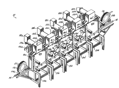
Figure 1 is a perspective view of a linear
transport system for a wafer processing line in
2s accordance with a preferred em~odiment of the invention.
Figure 2 is a cross-sectional side view taken
along lines 2-2 of Figure 1.
~137~71
W0-94/00868 ~ PCT/US93/06118
-8-
Figure 3 is a cross sectional front view taken
along lines 3-3 of Figure 2.
Figure 4 is a schematic which illustrates the
interconnections of a master controller to each of the
moveable parts of the transport mech~n;sr depicted in
Figure 1.
Figure 5 is a cross-sectional top view taken
along lines 5-5 of Figure 2.
Detailed Descri~tion of the Drawinqs
Figure 1 shows a transport system 10 for a
wafer processing line. The transport system 10 includes
a plurality of housings 12a, 12b, 12c, 12d and 12e which
are serially connected. The housings 12a-12e are
supported on rigid frames 13a-13e, respectively. A track
14 extends along and through the serially connected
housings 12a-12e. Though not shown in Figure 1, the
track 14 comprises a plurality of track segments 14a,
14b, 14c, 14d and 14e which correspond to housings 12a,
12b, 12c 12d and 12e, respectively.
Isolation valves 16 separate and isolate each
of the adjacently situated housings 12. The isolation
valves 16 open and close to permit and restrict,
respectively, access between adjacently situated housings
12 along the track 14. In Figure 1, isolation valve 16b
is located between housings 12a and 12b. Similarly,
isolation valve 16c is located between housings 12b and
12c. While Figure 1 shows six isolation valves,
designated by reference numerals 16a-16f, with one
2137~71 ~ =
WO94/00868 PCT/US93/06118
_9_
isolation valve 16 between every two adjacently situated
housings 12, it is to be understood that one or more of
these isolation valves 16 could be omitted at the entry
and exit ends of any one or more of the housings 12,
depending upon the vacuum conditions re~uired for wafer
processing. It is to be understood that additional
housings 12 may be connected in series. The total number
of housings 12 will depend upon the particular wafer
process that is being performed. The transport system 10
of this invention is advantageous with respect to a wafer
processing line which includes as few as one housing 12
and up to twelve or more housings 12.
Preferably, each of the housings is
evacuatable. Figure 1 shows vacuum pumps 18a-18e
connected to housings 12a-12e via conduits 20a-20e,
respectively. The vacuum pumps 18a-18e may be isolated
from the housings 12a-12e by gate valves 22a-22e,
respectively.
At least one wafer carrier 24 is linearly
translatable along the track 14 through the housings
12 when the isolation valves 16 are open. Figure 1 shows
a carrier 24a located adjacent the entrance to housing
12a and a second carrier 24b located adjacent the exit of
housing 12e. Each wafer carrier 24 includes a pair of
spaced, parallel and vertically oriented support members,
or pallets 26. The pallets 26 support wafers 27 during
wafer processing along the track 14. Preferably, to
m~imi ze throughput for a wafer processing operation, a
2137~71
W0 94/00868 PCT/US93/06118 ~
--10--
plurality of carriers 24 are synchronously translated in
linear fashion through the housings 12 along the track
14. The pressure in each housing 12 is controlled by its
corresponding vacuum pump 18, gate value 22 and the two
isolation valves 16 located at opposite ends thereof.
In each of the housings 12, a particular wafer
processing step is performed. Figure 1 shows wafer
processing units 28b and 29b mounted to one side of
housing 12b. Simiarily, wafer processing units 28c and
29c are mounted to one side of housing 12c, and wafer
processing units 28d and 29c are mounted to one side of
housing 12d. These wafer processing units 28 and 29 may
be adapted for performing cathode sputtering, sputter
etching, heating or any one of a number of other wafer
processing steps.
Figure 2 shows a cross sectional side view of
serially connected housings 12b and 12c. Track segments
14b and 14c are located within the housings 12b and 12c,
respectively. A space 31 is located between each of the
housings 12. More specifically, 31c space is located
between interconnected housings 12b and 12c. This space
31c is occupied by isolation valve 16c when the valve 16c
is closed to isolate the housings 12b and 12c from each
other. The cross sectional ~;~Pncions o~ this space 31C
are slightly greater than the cross sectional ~i~P~sion
of the wafer carrier 24. When the isolation valve 16c is
open, the space 31c is empty and the carrier 24 may move
2137471
~ W094/00868 PCT/US93/06118
--11--
through space 31c along the track 14 from housing 12b to
housing 12c.
To move the wafer carrier 24 through housing
12b, through space 31c and into housing 12c, and along
the track 14 between the other interconnected housings
12, the carrier 24 is equipped with a plurality of
magnets 34. The magnets 34 are aligned substantially
parallel with track segment 14b and mounted to the bottom
of a base 36 of the wafer carrier 24. As shown in Figure
3, the base 36 is supported above a nonmagnetic bottom
wall 38b of housing 12b by wheels 40 located on opposite
sides of the carrier 24. The wheels 40 rotate on axles
41 which extend outwardly from opposite sides of the base
36. The wheels 40 ride on the bottom surfaces of C-
shaped ch~nnels 42. The tops of the channels 42 are
spaced above the tops of the wheels 40. Preferably, four
equidistantly spaced sets of wheels 40 are provided for
each carrier 24, though three sets or even five sets or
more would also be suitable.
With four spaced sets of wheels 40, the center
of gravity of the carrier ~4 remains above a center axis
44 through the vertical pallet 26. The carrier 24 also
includes a central support member 43 which rotatably
supports the pallets 26 on an axle 45. Because of the
weight distribution of the carrier 24 and the four setsof wheels 40, the carrier 24 cannot tip forwardly or
rearwardly as a forward set of the wheels 40 extends into
the space 31c between track segments 14b and 14c.
2137471
-12-
Additionally, tops of the C-shaped channels 42 will
prevent forward or rearward tilting of the carrier 24 as
it moves across the discontinuity in the trac~ 14 between
the adjacently situated housings 12.
To linearly translate the carrier 24 along the
trac~ 14, the transport system 10 includes a plurality of
magnetic drive units 46, with one magnetic drive unit 46
corresponding to each of the housings 12. According to
one embodiment, the magnetic drive unit 46 includes an
endless loop conveyor 48 driven by a motor 49 with a
plurality or magnets S0 mounted to the outside of the
conveyer 48. For each of the housings 12, a magnetic
drive unit 46 is located outside of the housing 12, and
the conveyor 48 is aligned parallel with the respective
trac~ segment 14. As shown in Figure 3, the magnets 50
mounted on the conveyor 48 are aligned with the maqnets
34 mounted on the carrier 24, with the nonmagnetic
bottom wall 38 of the housing 12 located therebetween.
The magnets 50 impose a plurality of magnetic fields
within the housing 12. Preferably, the thic~ness of the
0.635c~
wall 38 is about (1/4 inch)and the distances from the
magnets 34 to wall 38 and the magnets 50 to the wall 38
0~3l~
are both about (1/8 inc~.
When the motor 49 drives the conveyer 48, the
~5 magnetic fields imposed in the housing 12 move linearly
along the trac~ 14. Because of the magnetic coupling
between the magnetic fields from the magnets S0 of the
magnetic drive unit 46 and the magnets 34 on the carrier
~-- =
~ W O 94/00868 213 7 ~ 71 PC~r/US93/06118
.
--13--
24, movement of the conveyer 48 causes carrier 24 to move
along the track 14. Because this transport system 10
uses no intermeshed gears or frictional couplings or
connections, the carriers 24 are linearly translated in
5 an environment which is, for all practical purposes,
particulate free. While there is some me~hAn;cal contact
between the wheels 40 and the C-ch~r~ channels 42, the
wheels 40 are substantially surrounded by the channels 42
and located below the wafer holding pallet 26. Finally,
lo because the wafers 27 are mounted to pallet 26 in
vertical orientation, the possi~ility of any particulate
settling on wafers during processing is further
minimized.
Alternatively, the carrier 24 could be
15 translated along the track 14 via magnetic levitation by
permanent magnets or electromagnets mounted inside the
housings 12.
While the embodiment shown in Figures 2 and 3
involves a magnetic drive unit 46 which employs an
20 endless belt conveyer 48, it is to be und~rstood that the
invention contemplateS: various alternative embodiments
for imposing a plurality of magnetic fields within the
housings 12 and moving the imposed magnetic fields with
respect to the housing 12 for the purpose of linearly
25 translating the carrier 24 along the track 14
therethrough. For instance, the magnets 50 could be
moved by a rack and pinion mechanism, or by a nut and
2137~7'1
WO94/00868 PCT/US93/06t18
-14-
screw arrangement with a long screw rotated by a motor to
drive the nut linearly.
As shown schematically in Figure 4, a master,
programmable controller 52 coordinates movement of all of
the moveable parts of the transport system 10 of this
invention. Preferably, the controller 52 is a
microprocessor or a PLC device. ~he controller 52
operatively connects to a plurality of motor controllers
54, each of which controls the operation of a motor ~9 of
one of the magnetic drive units 46. The controller 52
also connects to motor controllers 17a-17f which operate
isolation valves 16a-16f, respectively. The controller
52 also connects to controllers l9a-19e which operate
vacuum pumps 18a-18e, respectively, and motor ~o~ ollers
23a-23e which operate gate valves 22a-22e, respectively.
The controller 52 coordinates operation of all
of these components according to a desired sequence. A
plurality of carriers 24 may be moved along the track 14
and through the housings 12 in synchronous fashion, or
independently, depending upon the total number of wafers
27 which must be processed along the line according to a
particular sequence of steps.
As shown in Figure 5, the transport system 10
of this invention also contemplates rotation of the
pallets 26 during certain wafer processing steps, such as
sputter coating or sputter etching. By rotating the
pallets 26 during processing, uniformity in wafer coating
is achieved. Rotation of the pallets 26 during
~ 2137471
-15-
processing may be continuous, or it may be performed
stepwise by indexing the pallet 26 into alignment with
the wafer processing units 28 and 29. In certain types
of wafer processing, stepwise indexing of the pallets 26
is advantageous. For instance, during sputtering,
indexing the pallets 26 to align the wafers 27 with the
wafer processing units 28 and 29 rp~llres the amount of
sputtered material which deposits on the side surfaces of
the pallet 26, rather than on the wafers 27. Eventually,
this material which deposits upon the pallets 26 instead
of the wafers 27 must be cleaned off, resulting in down
time for the system 10.
Figure 5 sh.ows the structural components which
perform pallet rotation. More particularly, a rotational
magnetic drive unit 65 is located outside of housing 12.
This rotational drive unit 65 is aligned along the axis
44 of the pallet 26 when the carrier 24 is in a
processing position within the housing 12. The drive
unit 65 includes a motor 67, a shaft 69 and magnets 71
mounted to a forward end of the shaft 69. The magnets 71
are located proximate an outer surface of a nonmagnetic
vertical wall 72 of the housing 12. The pallet 26 also
includes magnets 74 mounted proximate the interior
~ surface of the wall 72. o,63
Preferably, the wall 72 is about~/4 inc~
thick, and the distances between magnets 71 and wall 72
~ 3l8c~
and magnets 72 and wall 72 are both about (1/8 inc~ To
vary the strength of the magnetic fields imposed by the
wo 94~oo8682 1 37 4 7~ PCT/US93/06118 ~
-16-
magnets 71, the magnetic drive unit 65 is moveable along
axis 44 toward and away from the housing 12, as shown by
directional arrows 75. Pistons 76 located between the
two wafer processing units 28 and 29 may be used to move
the magnetic drive unit 65 toward and away from housing
12 along axis 44.
During processing, the rotational magnetic
drive unit 65 is located in its forward position, as
shown in Figure 5, and magnetic fields imposed in the
housing 12 by the magnets 71 magnetically couple with the
magnets 74 of the carrier 24. Operation of the motor 67
rotates the shaft 69 to rotate the magnets 71, thereby
rotating the imposed magnetic fields. Rotation of the
imposed magnetic fields rotates the magnets 74, thereby
causing the pallets 26 to rotate. Thus, by controlling
operation of the motor 67 to rotate the shaft 69, either
continuously or in indexing fashion, the pallets 26 can
also be rotated. This moves the wafers 27 relative to
the wafer processing units 28 and 29 during processing.
Although only one rotational magnetic drive
unit 65 is depicted in the drawings, it is to be
understood that additional such drive units 65 may be
utilized in this transport system 10, with as many as one
unit 65 for each of the housings 12. The total number of
rotational drive units 65 will depend upon the number of
housings 12 which are dedicated to wafer processing steps
that require rotation of the pallet 26 to move wafers 27
relative to the wafer processing units 28 and 29. As
W094/00868 2 1 3 7 4 7 1 - PCT/US93/06118
-17-
with the linear magnetic drive units 46, the vacuum pumps
18, the isolation valves 16 and the gate valves 22, the
rotational magnetic drive units 65 and the pistons 76 are
preferably connected to the master col,L-oller 42 so that
rotation of the pallets 26 is coordinated with the
movement of the carriers 24 and the isolation of the
housings 12, according to a pre-determined sequence of
operation.
While these and other features of a transport
system 10 in accordance with a preferred embodiment of
the invention have been described, it is to be understood
that the invention is not limited thereby and in light of
the present disclosure, various other alternative
embodiments will be apparent to one of ordinary skill in
the art without departing from the scope of the
invention. Accordingly, applicant intends to be bound
only by the following claims.