Note: Descriptions are shown in the official language in which they were submitted.
21~'~476
Docket No. 142-168P
AN IMAGE-FORMING DEVICE AND
AN IMAGE-FORMING ELEMENT FOR USE THEREIN
BACKGROUND OF THE INVENTION
Field of the Invention
The present invention relates to an image-forming
device and, more specifically, to an image-forming
configuration utilizing a novel image-forming element.
Discussion of Related Art
Image-forming devices of the nature herein discussed
and image-recording elements usable therein are described,
inter alia, in EP-A-0 191 521, EP-A-0 247 694 and EP-A-0
247 699. In these known devices, a toner powder image
formed on the image-recording element in an image-forming
zone is transferred directly, or indirecti'y via an
intermediate medium, to a receiving material, such as
ordinary paper, and fixed thereon. The image-recording
element can then be used again for the next image-forming
cycle. It has been found that in the known image-recording
elements a number of problems may arise which are related
to the electrical resistance of the image-forming
electrodes.
On the one hand, a low resistance can lead to an
excessive electrical current flowing through the
electrodes, and this may result in burn-out of the image-
forming electrodes. A burnt-out image-forming electrode
then no longer contributes to image-formation, and this is
~i3~~~s
2 Docket No. 142-168P
visible on the print in the form of a fine toner-free
streak in the image pattern. A burnt-out image-forming
electrode may, therefore, necessitate replacement of the
complete image-recording element. On the other hand, a
high resistance of the image-forming electrodes results in
such influence of the RC-circuit which, as a resistance
component, contains the control means and the image-forming
electrodes themselves and, as the capacitative component,
the image-forming zone, that the speed of the image-forming
process is very restricted. In addition, in an embodiment
of the image-recording element as described in NL-A-
9201892, wherein the control means consist of an array
fixed in the wall of a cylindrical element, the proportion
of the image-forming electrodes in the resistance component
varies as a function of the distance peripherally between
the position of the control means and the image-forming
zone. A high resistance of the image-forming electrodes
thus has an unacceptable effect on the total resistance.
Summary of the Invention
Therefore, it is an object of the present invention to
provide an image-forming device which will overcome the
above-noted disadvantages.
It is a further object of the present invention to
provide an image-forming device having an improved image
recording element, with which the problems occurring in the
known image recording elements are largely obviated.
The foregoing objects and others are accomplished in
accordance with the present invention, generally speaking,
by providing an image-forming device comprising a movable
image-recording element including a support with a
dielectric surface layer and, beneath the dielectric
surface layer, a set of separately energizable image-
forming electrodes insulated from one another, an image-
forming zone situated along the trajectory of the image-
recording element, in which zone a co-acting electrode is
213'~47~
3 Docket No. 142-168P
disposed a short distance above the dielectric surface of
the image-recording element, and control means in order to
apply a voltage between the image-forming electrodes and
the co-acting electrode in accordance with an image pattern
for recording, in order to selectively deposit toner powder
present in the image-forming zone on the surface of the
image-recording element in accordance with the image
pattern.
According to the instant invention, the image-forming
electrodes consist of an electrically conductive material
having an electrical resistivity of between 0.008 and 0.2
S2.cm. With such a resistance for the image-forming
electrodes, it has been determined that in the image
forming elements of the kind described in the above prior
art, wherein a voltage of 25 - 50 volts is applied to the
electrodes, there is no risk of the image-forming
electrodes burning out and a process speed of up to at
least 20 meters per minute can be obtained without
problems.
In another embodiment of the invention, the image-
forming electrodes are made by constructing the electrodes
as a number of grooves extending parallel to one another in
the direction of movement of the support for the image-
recording element, these grooves being filled with
electrically conductive material. The required electrode
resistivity of between 0.008 and 0.2 S2.cm is obtained by a
groove filling consisting of a first conductive layer on
the surface of the grooves and a second conductive layer
with which the remaining volume of the grooves is filled,
the resistivity of the first conductive layer being lower
by a factor of 0.125.103 - 2.103 than that of the second
conductive layer.
BRIEF DESCRIPTION OF THE DRAWINGS
The present invention will become more fully
understood from the detailed description given hereinbelow
4 Docket No. 142-168P
and the accompanying drawings which are given by way of
illustration only, and thus are not limitative of the
present invention, and wherein:
Fig.l is a diagram of an image-forming device
according to the invention;
Fig. 2 is a cross-section of an image-recording
element for use in the device of Fig. 1;
Fig. 3 is an enlarged scale cross-section in detail of
a first embodiment of an image-recording element on the
line III-III in Fig. 2; and
Fig. 4 is a similar cross-section of a second
embodiment of an image-recording element according to the
invention.
DETAILED DISCUSSION OF THE INVENTION
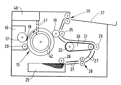
The image-forming device shown in Fig. 1 is provided
with the image-recording element 15, which is described in
detail hereinafter with reference to Fig. 2. The image-
recording element 15 passes through an image-forming
station 16, where its surface is provided with a uniform
layer of toner powder having a resistivity of about 1O5S2.cm
by means 20 constructed as described in U.S. Patent
3,946,402.
The powdered surface of the image-recording element 15
is then fed to an image-forming zone 18, where a magnetic
roller 17 is disposed at a short distance from the surface
of the image-recording element 15, the roller 17 comprising
a rotatable electrically conductive non-magnetic shell and
a stationary magnet system disposed inside the shell. The
stationary magnet system comprises a ferromagnetic knife
blade clamped between like poles of two magnets and is
constructed as described in EP-A-0 304 983. A powder image
is formed on the- image-recording element by the application
of a voltage between one or more image-forming electrodes
of the image-recording element 15 and the conductive shell
of the magnetic roller 17 operative as the co-acting
Docket No. 142-168P
electrode. If no image is recorded, the magnetic roller 17
and the image-forming electrodes of the image-recording
element 15 are maintained at earth potential. During
image-recording the image-forming electrodes involved are
5 brought to a positive potential of about 30 volts. This
powder image is transferred, by the application of
pressure, to a heated rubber-covered roller 19. A sheet of
paper is taken from a supply stack 25 by roller 26 and is
fed via paths 27 and rollers 28 and 29 to a heating station
30. The latter comprises an endless belt 31 running around
a heated roller 32 in the direction of the arrow. The
sheet of paper is heated by contact with the belt 31. The
sheet of paper thus heated is then fed between roller 19
and a pressure roller 35, the softened powder image on
roller 19 being completely transferred to the heated sheet
of paper. The temperatures of the belt 31 and the roller
19 are so adapted to one another that the image fuses to
the sheet of paper. The sheet of paper provided with an
image is fed to a collecting tray 37 via conveyor rollers
36.
Unit 40 comprises an electronic circuit which converts
the optical information of an original image into
electrical signals which are fed, via wires 41 provided
with trailing contacts, and conductive tracks 42 disposed
in the side wall of the image-recording element 15, to the
control elements 3 (see Fig. 2) connected to the tracks 42.
The information is fed serially line by line to the shift
register of the integrated circuits of the elements 3. If
the shift registers are completely full in accordance with
the information of one line, that information is put in the
output register, and electrodes 6 and 5 (see Fig. 2) then
receive voltage via the drivers or not depending on the
signal. While this line ~s printed the information of the
next line is fed to the shift registers. Apart from
optical information originating from an original,
electrical signals originating from a computer or a data
21~'~~'~~
6 Docket No. 142-168P
processing system can also be converted in the unit 40 to
signals fed to the control elements 3.
The image-recording element used in the image-forming
device.according to Fig. 1 is shown in diagrammatic cross
section in Fig. 2. The image-recording element 1 according
to Fig. 2 comprises a cylinder 2 having disposed therein an
axially extending control element 3 having a construction
which will be described in detail hereinafter. The
cylinder 2 is covered with an insulating layer 4 on which
image-forming electrodes 5 are applied extending in the
form of endless paths parallel to one another at
substantially equal spacing in the peripheral direction of
cylinder 2. Each image-forming electrode 5 is conductively
connected to one of the control electrodes 6 of the control
element 3. The number of control electrodes 6 of the
control element 3 is equal to the number of image-forming
electrodes 5, such number determining the quality of images
to be formed on the image-recording element 1. Image
quality improves with increasing electrode density. To
achieve good quality, the number of image-forming
electrodes 5 is at least 10 per millimeter and preferably
14 to 20 per millimeter. According to one specific
embodiment, the number of electrodes 5 is equal to 16 per
millimeter, the electrodes 5 having a width of 40 ~m and
the spacing between the electrodes being about 20 ~,m.
Finally, the pattern of image-forming electrodes 5 is
covered by a smooth dielectric top layer 7. In order to
prevent burn-out of the image-forming electrodes and undue
limitation of the image-forming device processing speed,
the image-forming electrodes consist of an electrically
conductive material having a resistivity of between 0.008
._ and 0 . 2 t2 . cm .
The control element 3 comprises a support 10 provided
in a known manner with an electrically conductive metal
layer (such as copper), which metal layer is converted to
the required conductive track pattern 12 in the manner to
213' ~'~
7 Docket No. 142-168P
be described hereinafter. The track pattern 12 consists,
on the one hand, of the conductive connections between the
various electronic components 13 of the control element
and, on the other hand, the control electrodes 6 which are
each conductively connected to one of the image-forming
electrodes 5. Finally, the control element 3 also
comprises a cover 14 connected in a manner known per se
( a . g . some adhesive ) to the support 10 to form a control
element 3 in the form of a box containing the electronic
components.
The electronic components 13 comprise a number of
integrated circuits (I.C.'s) known, for example, from the
video display technique, comprising a series-in parallel-
out shift register, an output register and, connected
thereto, drivers having a voltage range of, for example, 25
to 50 volts . Each control electrode 6 is connected to a
driver of one of the integrated circuits.
The image-recording element 1 is made as follows. A
control element 3 is made from a metal core substrate
consisting of an aluminum support sheet to which a copper
foil is glued by means of an electronic grade epoxy resin
specially developed for the electronics industry, the
copper foil being converted, by a known photo-etching
technique, into a conductive track pattern 12 which
comprises both the conductive connecting paths for the
electronic components 13 to be placed on the support 10,
and the conductive paths of the control electrodes 6. The
electronic components 13 are then fixed on the support 10
at the correct place defining the conductive connecting
paths and cover 14 is glued to the support 10 with an
electronic grade epoxy resin.
The box-shaped control element 3 made in this way is
then placed in an axial slot in the wall of aluminum
cylinder 2 and secured fast therein by means of the above-
mentioned epoxy resin glue. The axial slot is at least of
a length equal to the working width of the image-recording
8 Docket No. 142-168P
element 1. With regard to the width of the axial slot in
the cylinder 2, the space between the control element 3 and
the wall of the slot must be so dimensioned that such space
can be filled by the glue by capillary action. An
excessive space results in the glue running out.
The outer surface of the cylinder 2 with the control
element 3 fixed therein is turned on a lathe to a
predetermined size and brought into contact with a suitable
etching liquid (e. g. a known alkaline potassium
ferricyanide solution) so that the metal of the top layer
of both the cylinder 2, the support 10, and the cover 14 is
etched away over a specific depth, e.g. 150 Vim. The
etching liquid is so selected that the metal of the control
electrodes 6 is only slightly affected, so that the ends of
these electrodes finally project about 150 ~.m above the
surface of the cylinder 2 and the control element 3. The
surface of the cylinder 2 is then covered with an
insulating intermediate layer 4 of electronic grade epoxy
resin with a layer thickness equal to the length of the
projecting ends of the electrodes 6, so that the end
surfaces thereof lie at the outer surface of the insulating
intermediate layer 4. This is achieved by applying a
thicker intermediate layer 4 and then turning this layer on
the lathe until the end faces of the electrodes 6 are
exposed at the surface of the intermediate layer 4. The
image-forming electrodes 5 are formed (as shown in Fig. 3),
by cutting (e.g. on a lathe) a number of peripheral and
parallel endless grooves 50 in the outer surface of the
intermediate layer 4. The groove pattern is so applied
that it corresponds completely (in respect of density and
location) to the pattern of control electrodes 6, so that
each control electrode 6 co-operates with one groove. The
grooves 50 are filled with electrically conductive
material, thus forming the conductive image-forming
electrodes 5.
2~.~'~~7G
9 Docket No. 142-168P
In a first embodiment of the recording element
according to the invention, the grooves 50 in the
insulating intermediate layer 4 are filled by applying an
electrically conductive material over the complete surface
of the image-recording element to a layer thickness
indicated by broken line 51 in Fig. 3, and then turning
this layer of electrically conductive material on the lathe
down to the outer surface of the insulating intermediate
layer 4. The pattern of electrically conductive image-
forming electrodes 5, which are insulated from one another
by the intermediate layer 4, is finally covered with a
smooth dielectric top layer 7, which consists, for example,
of a SiOX layer of a composition as described in Netherlands
patent application 9301300.
In principle, any material having the required
electrical resistance can be used for the electrically
conductive material. Such a material may, for example,
consist of a binder in which conductive particles are
finely distributed, such as carbon, metal (copper or silver
particles), metal complexes, quaternary ammonium compounds
or conductive polymers or mixtures thereof.
If the above-mentioned SiOX is used as a dielectric
material for the top layer 7 interconnecting the image-
forming electrodes 5, an electrical resistance of between
0.008 and 0.5 S2.cm is necessary for the electrodes 5 to
achieve the required resistance of the electrodes 5, which
must be lower than the resistance of the top layer 7. The
control means to vary the electrical resistance when use is
made of an above-mentioned conductive paste, is the
quantity of conductive particles distributed in the binder
(e. g. an epoxy resin).
In a preferred embodiment illustrated in Fig. 4, the
conductive image-forming electrodes 5 are formed from a
combination of a thin metal layer 55 applied to the surface
of the grooves 50 and a conductive epoxy resin 56 with
which the rest of the grooves 50 is filled. The thin metal
z1~7~7s
Docket No. 142-168P
layer 55 appears to be a better control means for obtaining
the correct resistance value for the image-forming
electrodes 5 than the above-mentioned embodiment in which
conductive particles are finely distributed in the binder
5 (the epoxy resin). In principle, a number of materials
such as Cu, Ta, tantalum nitride and NiCr can be used for
the metal layer 55. Outstanding results have been obtained
with an 0.25 ~.m thick NiCr layer applied uniformly to the
groove pattern by means of the known sputter technique in
10 a vacuum installation, e.g. of the Balzers LLS 802 type,
NiCr being sputtered from an NiCr 30/70 target with a 99.9%
purity, argon and oxygen being introduced into the vacuum
installation.
A conductive epoxy resin is then applied to this metal
layer to give a layer thickness indicated by broken line 57
in Fig. 4. The epoxy resin used was a dispersion
consisting of 100 parts by weight of epoxy resin (Shell
Epikote 828 EL type), 10 parts by weight of latent hardener
(Ajinomoto MY-24) and 8.9 parts by weight of carbon of
Degussa Printex XE-2 type. Similarly to the embodiment in
Fig. 3, this epoxy layer (and in this embodiment also part
of the metal layer 55), is then turned on the lathe until
the insulating intermediate layer 4 is exposed at the
surface, between the grooves, whereupon the SiOX top layer
7 is applied as described hereinbefore.
One of the reasons why NiCr is a suitable material as
a metal layer arises out of the above-described production
method, wherein the part of the metal layer 55 indicated by
broken lines in Fig. 4 is also removed by turning. NiCr
proves to be much better to machine than other materials
such as Ta and tantalum nitride, which are suitable for
electrical reasons.
With the above-described 0.25 ~m NiCr layer in
combination with the conductive epoxy resin a resistivity
of 0.1 S2.cm is obtained, which is within the limits of the
required resistivity (0.008 - 0.2 S2.cm). In the event of
~~3'~4'~6
11 Docket No. 142-168P
a change of the electrical properties of the conductive
epoxy resin 56 or the dielectric top layer 7, it may be
necessary to adapt the resistivity of the metal layer 55 to
some extent. Such adaptation can ba obtained fairly simply
with the following control means: the composition of the
NiCr target, the quantity of oxygen doped during sputtering
and the process time for sputtering so that a different
layer thickness is achieved. The influence of these
control means is.such that a larger quantity of Cr in the
target and/or more oxygen doping gives a higher resistance
and a longer process time and hence a greater layer
thickness gives a lower resistance.
The above description describes the use of different
types of epoxy resins in a number of applications. On the
one hand, the epoxy resin is used as glue for sticking
together a number of parts of the control element 3 (the
copper foil in which the conductive track pattern 12 is
formed on the aluminum support 10 and the cover 14 on the
support 10) and for gluing the control element 3 securely
in the axial slot of the aluminum cylinder 2. On the other
hand, a different type of epoxy resin is applied to the
surface of the aluminum cylinder 2 in order to provide the
insulating intermediate layer 4.
In all these applications, good adhesion of the epoxy
resin to the metal components (aluminum or copper) is very
important. It has been found that this adhesion can be
considerably improved by dispersing in the epoxy resin core
shell powder particles consisting of a core of rubber (e. g.
butyl acrylate or butadiene/styrene) with a shell of
acrylic resin therearound (e. g. polymethylmethacrylate).
Core shell powder particles of this kind are marketed inter
alia by Rohm & Haas under the name Paraloid EXL for
improving the mechanical properties (e. g. impact strength)
of thermoplastics. A modified epoxy resin with excellent
adhesion properties can be prepared, for example, by
homogeneously distributing with means known per se 5 - 20
12 Docket No. 142-168P
parts by weight of the above-mentioned core-shell powder
particles (Paraloid EXL 2600 type) having a particle size
of 0.2 ~m in 80 - 95 parts by weight of epoxy resin (Epoxy
Technology Epotek 377 type).
The present invention being thus described, it will be
obvious that the same may be varied in many ways. Such
variations are not to be regarded as a departure from the
spirit and scope of the invention, and all such
modifications as would be obvious to one skilled in the art
are intended to be included within the scope of the
following claims.