Note: Descriptions are shown in the official language in which they were submitted.
7 ~ ~ ~
- DYNAMICALLY PROGRAMMABLE TIMER-COUNTER
Backqround of the Invention
The present invention relates to a timer circuit,
and more specifically, to a method of programming a
programmable timer circuit for an integrated circuit
arrangement.
It is known to use a programmable timer counter
within an integrated circuit arrangement. In one such
conventional circuit arrangement, a programmable micro-
processor is in bus communication with an applicationspecific integrated circuit (ASIC). It is known to
comprise the ASIC of a plurality of interconnected
integrated circuit modules for performing various
signaling functions. One such module of the ASIC can
be an address decoder and programmable timer. To program
the timer, the microprocessor addresses a specific ASIC
address and latches the appropriate timer data on the
data bus. The ASIC responds to enable the writing of the
timer data into the timer counter and then enables the
timer counter to count out. Programming of the timer
counter in this manner restricts waiting to the timer
counter to a period within the timer has time-out.
Summary of the Invention
It is an objective of an aspect of the present
invention to present a microprocessor control system
employing a microprocessor in bus communication with an
ASIC and a plurality of memory units, the ASIC having a
count programmable timer module which count can be
programmed independent of timer count.
~ ~ ~ 7 5 ~ ~
~_ - 2 -
It is an objective of an aspect of the present
invention to present a microprocessor control system
employing a microprocessor in bus communication with an
ASIC and a plurality of memory units, the ASIC having a
count programmable timer module which count can be
programmed independent of timer count and which timer
can be programmed to operate in either a continuous or
one-shot mode.
An aspect of the invention is as follows:
A programmable timer circuit comprising: program-
mable timer counter means having input means for
receiving a count for counting to said count and for
receiving a periodical clock signal and counting to said
count in response to said clock signal for generating a
signal representative of said count, a programmable means
for generating count data in response to programming of
said programmable means, timer data register means for
receiving said count from programmable means, first gate
means having an enabled mode and a non-enabled mode for
enabling loading of said timer data from said timer data
register to said timer counter input means only in said
enabled mode, monitoring means for monitoring said timer
count and enabling said gate means to said enabled mode
only when said timer has time-out.
The microcontroller system is comprised of a micro-
processor which is in bus communication with a number
of memory units and an ASIC. The ASIC includes a
.
7 5 ~ ~
number of system modules, for example, a non-
volatile memory security module, a printhead control-
ler module, a pulse width modulation module, etc. One
of the modules of the ASIC is a timer circuit module.
The timer circuit module includes a plurality of
registers which can be addressed to enable writing of
timer data into the module. One of the timer registers
is a timer control register and an input data register
is also included. In response to data written in the
timer control register, a continuous or one-shot mode
is selected and, also, the timing period. The timer
circuitry either enables the system clock to clock the
timer single time-out in the one shot mode or
sequentially re-enables the system clock to clock the
timer for an uninterrupted second and subsequent time-out
by retriggering. During retriggering of the timer, timer
data written to the timer input registers is reloaded to
the timer.
The timer data register and the timer control
registers can be accessed for writing of timer data
into each register by the microprocessor through an
ASIC decoder circuit and data bus independently of
timer count. A gate restricts loading of the timer
count to the timer counter until timer count time-
out is reached, at which point, a signal is produced
which enables the gate to allow the timer count in
the timer data register to be loaded into the timer
counter. Also, a timer output register is in
. ~. 3,
2137511
-- 4
communication with the timer count output count which enables the timer count to be
read by the microprocessor for status checking. Further, the timer data pl esellLly in the
timer data register may be read by the microprocessor at any time upon enabling by the
microprocessor of a second gate means.
It should be appreciated, that the progl ~ llable timer circuit offers the benefit
of allowing the microprocessor to write timer data at any opportune time with concern
for or disturbing the timer count. It is also beneficial for the microprocessor to be able
to confirm the timer count data written to the timer data register and to monitor the
timer count at any time independent of the timer count. Other advantages of the
present invention should be appreciated from the following detailed description.
Brief Description of the Drawings
Fig. 1 is a schematic of a microprocessor control system including an ASIC in
accordance with the present invention.
Fig. 2 is a schematic of a timer circuit in accordance with the present invention.
Fig. 3a is a process flow diagram for setting ofthe timer in accordance with thepresent invention
Fig, 3b is a process flow diagram for ch~nging the setting of the timer in
accordance with the present invention
Fig. 3c is a process flow diagram for reading the setting ofthe timer in
accordance with the present invention
Fig. 3d is a process flow diagram for ch~nging the timer mode of the timer in
accordance with the present invention
21~7~11
Fig. 4 is a process flow diagram of the timer enable circuit in accordance with
the present invention.
Fig. 5 is a process flow diagram for starting and re-starting the timer in
accordance with the present invention
Detailed Description ofthe Plerel,ed Embodiment
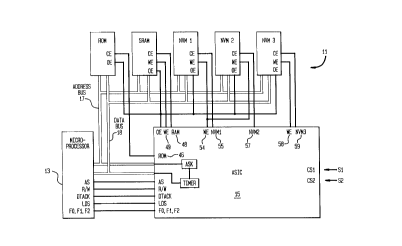
Referring to Fig. 1, a micro-controller system, generally indic~ted as 11, is
comprised of a microprocessor 13 in bus 17 and 18 communication with an application
0 specific integrated circuit (ASIC) 15, a read only memory (ROM), a random access
memory (RAM) and a plurality of non-volatile memories (NVM1, NVM2, NVM3).
The microprocessor 13 also communicates with the ASIC 15 and memory units by
way of a plurality of control line, more particularly described subsequently. It should
be appreciated that, in the prerelled embodiment, the ASIC 15 includes a number of
circuit modules or units to perform a variety of control function related to theoperation ofthe host device, which, in the present p~;relled embodiment, the host
device is a postage meter mailing machine.
Referring to Figs. 2 through 5, the timer circuit will be described in accordance
with the timer process flow diagrams. In order to set the 1 6-bit timer, the
microprocessor addresses the ASIC decoder 20 and latches the timer data on the data
bus 17. The address decoder 20 then enables the write signal which then allows the
timer data on the data bus 17 to be loaded into the input register 600 and mode data
into the timer control register 602. The mode data is that data which enables the timer
for continuous mode or a one-shot mode which will be further described later. After
21~7511
;, .~
-- 6
the data is loaded into the input register 600, the address decoder 20 then enables the
RDB signal which enables gate 604, which then enables the microprocessor to read the
data and compare the data such as to confirm that the proper timer data has beenwritten to the timer input register 600.
In order to enable the timer 622, the timer control register 602 is enabled by
the TCR6 signal from the timer control register 602 which enables the internal enable
signal. This signal is delivered to multiplexer 608 whose output then enables the flip-
flop 612. The output of flip-flop 612 enables OR gate 614 and flip-flop 618. Theoutput of flip-flop 616 enables gate 620 which enables loading of data from the input
0 register 600 into the 16-bit timer 622. The output of flip-flop 616 also is directed to
gate 619 to clear flip-flop 612 which signals the completion ofthe timer data load.
Referring back to the output of flip-flop 612 which enables flip-flop 618, the
multiplexer 624 is set to be continuously enabled or to be one-shot enabled by the C
mode signal from the timer control register 602. In the single shot mode the input of
the multiplexer 624 is set to receive the output from flip-flop 618. In the continuous
mode, the input of the multiplexer 624 is set to receive a continuous enable (EN).
Optionally, the timer enable signal can be supplied externally to allow measuring
intervals of events.
As noted, if the multiplexer 624 has been set to the one-shot mode, then the
output of flip-flop 618 is the input signal to the multiplexer 624. The output of the
multiplexer 624 enables flip-flop 626 which is AND to a clock signal by AND gate628. The output from flip-flop 626, in colllbinalion with the clock signal, drives the
clock input of the 16-bit timer 622. At this point, timer enable is complete and the
timer is initi~ted for counting. When the timer 622 reaches the set bit count loading to
2137~11
-- 7
the timer counter 622 from the input register 600, OR gate 630 goes active. When the
OR gate 630 goes active, the output from the OR gate 630 drives OR gate 632 which
in turns drives the flip-flop 642 active. The output from flip-flop 642, through an OR
gate 644, drives flip-flop 650 to issue an interrupt to the microcontroller system to
indicate that the timer has timed out. If a one-shot mode is selected, then the output
from flip-flop 642 also drives an AND gate 646 which goes active to clear flip-flop
618. Once flip-flop 618 is cleared, the AND gate 628 goes inactive, thereby stopping
clocking of the 16-bit timer counter 622.
If a continuous mode has been selected then the output of OR gate 630 drives
OR gate 614 active. The output from OR gate 614 drives flip-flop 616 active which
then actuates the gate 620 which enables reloading of data from the input register 600
into the 16-bit counter. The output from flip-flop 616 is again directed to gate 619 to
clear flip-flop 612 and the timer load is complete, and the timer then starts counting
again. The enable signal to the multiplexer 624 is continuous, therefore, the clock
signal provided at AND gate 628 is continuously provided to clock the timer 622.In order to change the 16-bit timer setting, it is not necessary to disturb the
count. While the timer is running, the microprocessor 13 can address the decoder 20
and latches the new timer input data on the data bus. The address decoder 20 then
enables the TIRB signal. When the TIRB signal goes active, the new timer data isloaded into the input register 600 and new mode data into the timer control register
602. Verification of the new timer data can be accomplished by since gate 604 isenabled by the TRIB signal which allows the data written into the input register 600 to
be read by the microprocessor through gate 604.
21~751~
-- 8
It is also possible to read timer data from a timer output register 600 without
disturbing the timer count of the timer 622. In order to read the timer setting, it is
necessary that the microprocessor 13 address the address decoder 20, the addressdecoder 20 then read/enables the timer output register 606 by enabling the TROB
signal which places the data which is in the timer register 606 on the data bus for
reading by the microprocessor 13.
The timer mode can also be changed independently when the microprocessor
addresses the decoder 20 and latches the timer control data on the data bus. Theaddress decoder 20 then write/enables the timer control register 602 by enabling the
0 TCRB signal for writing of new mode data into the timer register. It should now be
appreciated that the present invention allows for the timer to be set to either
programmable and selectable to be either single or continuous mode of operation.