Note: Descriptions are shown in the official language in which they were submitted.
2137531
~,J
. .
13-283
CAPACIT~VE T~RES~OLD DEI ECTOR TEST CIRCUIT
Field of the Invention
The present invention concerns a liquid level monitoring circuit and, more
particularly, a test feature of the monitoring circuit that allows operation of the
circuit to be confirmed.
Background Art
Robertshaw Controls Co., assignee of the present invention, sells a liquid
level sensor for detecting the presence or absence of a liquid and providing an
output that activates an alarm. This prior art sensor is sold under the designation
Mini-Tek 800. The Mini-Tek 800 sensor has a probe that determines a liquid levelat a probe site by monitoring capacitance changes caused by changes in liquid
level.
U.S. Patent No. 4,224,606 discloses a fluid level control circuit having a test
function. Pressing a test switch reduces voltage at an FET gate and takes the FET
from a pinched-off condition allowing a drain capacitor to discharge through theFET. This drops a relay out of the circuit and closes an alarm contact to actuate
an alarm.
U.S. Patent No. 4,676,100 discloses a test circuit for simulating a "high"
material level in an LC resonant frequency fluid level indicator. Closing a switch
activates a second switch and adds three capacitors in parallel with the probe.
The increased capacitance c~uses a threshold detector to indicate a "high" milteri;ll
level.
U.S. Patent No. 5,121,632 discloses a sensor including a self-cliagnostic
routine which connects the probe to a comparator that compares the voltage on
the probe to a supply voltage. Under normal conditions, the variable capacitanceof the probe will charge up to a supply voltage. If the probe is shorted, then the
variable capacitor will not charge up and cause the output of the comparator to be
high to flag and error condition on a microprocessor controller.
The present invention concerns a test circuit for use in conjunction with a
sensor such as the prior art Mini-Tek 800. A test input allows an operator to
~ 2137S3l
,
artificially simulate a condition which normally would cause the circuit to activate
an alarm. By activating the test input, the circuit's operation can be confirmed.
Disclosure of the Invention
The present invention includes a level detector that includes a first charging
circuit having a probe that can be placed at a liquid detection site and that charges
at a rate dependent upon the liquid level at the detection site. A second reference
charging circuit conducts charge at a rate independent of the liquid level at the
detection site. A control circuit compares the rate of charging of the first andsecond charging circuits and produces a detector output signal based upon the
colllyalison. Under normal circumstances, this output activates an alarm callingattention to the fact that the liquid has reached a certain level at the detection site
or alternately that no liquid is sensed at the detection site.
A test circuit inhibits one of the first and second charging circuits. This
artificially produces an alarm output since the comparison conducted by the
control circuit always results in a sensing of an alarm condition. In an instance in
which the probe warns when liquid is sensed, the test circuit artificially causes the
control circuit to sense liquid.
The preferred charging circuits include a switch coupled to the control
circuit which normally conducts when activated by the control circuit. The test
input inhibits the switch so that the control circuit senses a condition which
normally would cause an alarm. When a user manually activates thc test inr)ut ~othe detector, an alarm should result and if it does ~Ot, the cletector is no~ worki
properly.
The preferred de~ec~or includes fiel(J ellcc~ ~ransis~ors in bo~h ~l~c firs~ andsecond charging circuits. The field effect transistors are normally biased in
saturation, allowing normal charging of both the first and second circuits. A gate
electrode to one of the field effect transistors is selectively grounded by the test
input. When this occurs, the field effect transistor no longer charges at its normal
rate. Since the second circuit continues to charge at its normal rate, the control
circuit detects an alarm condition and produces an alarm output.
Z~37531
In accordance with the preferred design, the control circuit causes the first
and second charging circuits to conduct at regular intervals. Within a short time of
actuation of the test input, the detector should produce an output to activate an
alarm and confirm normal detector operation.
From the above, it is apparent that one object of the invention is a detector
for monitoring liquid levels having a test feature to enable a user to confirm
operation of the detector. This and other objects, advantages and features of the
invention will become better understood from a detailed description of a preferred
embodiment of the invention which is described in conjunction with the accom-
panying drawings.
Brief Description of the Drawings
Figures 1 and 2 are elevation views of two level sensors having test inputs
for confirming operation of the sensors;
Figure 3 is a schematic showing a circuit constructed in accordance with the
invention coupled to a probe at a liquid level test site;
Figure 4 is a schematic showing a control circuit for charging first and
second charging circuits with constant current and monitoring a voltage signal
produced by this charging;
Figure S is a portion of a probe-charging circuit showing an FET having a
gate coupled to a voltage source through a resistor; and
Figure 6 is a portion of the probe-char~ing circuit depicted in l~igl~re S with
the gate input grounded to initiate a test ot` th~ level sellsor.
Best Mode for Practicin~ the Invention
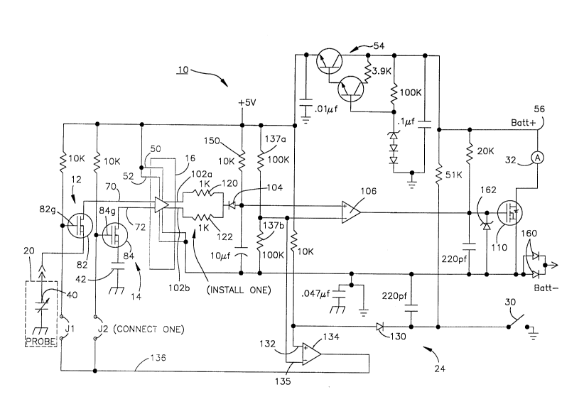
The drawings illustrate a level detector 10 that includes first and second
charging circuits 12, 14 (Figure 3) coupled to a control circuit 16 for monitoring
the presence or absence of fluid at a detection site. The first charging circuit 12
includes an elongated probe 20 that extends away from a base 22 (Figure 1) that
encloses the charging circuits 12, 14 and control circuit 16. Electrical signals are
routed into and out of the base 22 by a four pin connector 23 at the top of the
`~ ~137!~31
base. Pin contacts are not visible but are contained within a cavity in the
connector 23.
Operation of the first charging circuit ~2 is modified by a test circuit 24
coupled to one of the two charging circuits 12, 14. The test circuit 24 includes a
5 user-actuable switch 30 for allowing the user to test performance of the detector
10 and specifically, actuate a visual alarm 32 coupled to the control circuit. The
control circuit 16 includes circuitry for periodically activating the two charging
circuit 12, 14. Charge from the control circuit 16 builds up on capacitors 40, 42
causing voltages on the capacitors to increase at a rate dependent upon the
10 capacitance of the capacitors 40, 42. A charging current is most preferably
developed within the control circuit 16 which, in accordance with the preferred
embodiment of the present invention, is constructed using an ASIC (application
speci~lc integrated circuit). By determining which one of the first and second
charging circuits 12, 14 charges more quickly, the control circuit 16 can determine
15 an absence of or presence of liquid in contact with the probe 20.
Referring to the Figure 3 schematic, it is seen that two inputs 50, 52 to the
control circuit 16 are coupled to a power supply voltage of five volts. The five-volt
signal is maintained by a regulator circuit 54 coupled to a power input 56 whichtypically falls in a range of from 9-32 volts d.c. One use of the invention is for
20 monitoring fluid levels in a motor vehicle and the input 56 in this application is
battery voltage.
T}le five-volt signal at the inputs sn, 52 is coupled to two constant current
sources 60, 62 (Figure 4) having control gates cour)lecl ~o a control o~l~p~l~ 64 fro
a starter circuit 66. One constant current source 60 is coupled to an output 70 to
25 the first charging circuit 12 and a second constant current source 62 coup]ecl to an
output 72 to the second charging circuit 14. Upon actuation by the starter circuit
66, the current sources 60, 62 charge the two capacitors 40, 42 with a constant
current. The voltage build-up on these two capacitors, however, depends upon
their capacitance so that the voltage at two inputs 74, 76 to an operational
30 amplifier 80 in the control circuit 16 increases at different rates.
The lower the capacitance, the faster the charging occurs so that the
capacitor with the lower capacitance increases in voltage at the higher rate.
~137~3~
_` ~
s
As seen in Figure 3, current from the control circuit 16 charges the capac-
itors 40, 42 through two field effect transistors 82, 84. I)uring normal level
sensing, these field effect transistors 82, 84 have their gates 82g, 84g pulled up to
the five-volt power supply signal coupled to the control circuit inputs 50, 52. Thi~
S biases the FETs into saturation, allowing charging current from the control circuit
16 to flow through the FETs 82, 84 with a minimal voltage drop to an associated
one of the two capacitors 40, 42.
The current sources 60, 62 charge the charging circuits 70, 72 until the
charge on one of the capacitors 40, 42 reaches a two-volt threshold, after which a
10 discharge circuit 90 discharges them to ground. A cycle of capacitor charging and
discharging is maintained at a typical rate of 200 KHz so long as a voltage input
56 is applied to the level detector. The charge/discharge cycle rate is a function of
the smaller capacitance of the two charging circuits 70, 72.
Theory of Operation
The detector 10 depicted in Figure 1 is constructed for monitoring the
presence or absence of a conductive liquid. Detection of liquid level is ac-
complished by relating the level of liquid on the probe 20 to a change in capac-itance of the probe. This can be theoreticall~ evaluated by analogyzing to a
parallel plate capacitor in which one plate of the capacitor increases in size while
the second plate and the dielectric layer between plates remains a constant. As
the length of the probe 20 is emersed within the liquid changes, the plate size of
the theoretical capacitor increases and decre~lse.s. When the probe 2n is fully
emersed in liquid, thc cilp.lci~clnce rcach~s a Ill;lXill1llnl 1111~i ~ICCOrdillbly, Ihe
capacitor 40 charges less quickly Thus, in a situation in which the control circuit
16 monitors the absence of a liquid, as the amount of liquid overlap on the probe
20 decreases, the capacitance of the probe decreases so the time it takes the
capacitor 40 to charge increases. The capacitor 42 is a fixed value and does notchange with liquid level. It is used as a reference to compare the rate of charging
of the capacitor 40.
Level Sensing
The control circuit 16 senses voltages at the two connections 70, 72
by means of the operational amplifier 80. The operational amplifier 80 is
7 S3 1
configured as a differential amplifier so that an output 92 will be high if the signal
at the input 76 is greater than the input 74 and low otherwise. The output 90
from the amplifier 80 is clocked into a latch 100 by the discharge circuit 90 at the
end of every charge cycle. Outputs from the comparator 80 are transferred
through the latch circuit 100 to two complementary outputs 102a, 102b external to
the control circuit 16. A low signal from one of the outputs to a diode 104 wil]forward bias the diode 104 pulling a non-inverting input to a comparator 106
(Figure 3) low. This produces a low output from the comparator 106. The
comparator output is coupled to a gate input of an N channel MOSFET 110. A
low gate signal turns off the MOSFET 110 and de-activates the alarm 32. A high
signal from one of the outputs 102a, 102b will reverse bias the diode 104, allowing
the non-illvel lillg input of the comparator 106 to pull high. This produces a high
output from the comparator 106, turning the MOSFET 110 on, activating the
alarm 32.
With the probe fully emersed in liquid, the capacitor 40 has a greater
capacitance than the capacitor 42 and the voltage on the capacitor 42 increases
faster than the voltage on the capacitor 40. Referring again to the schematic ofthe control circuit 16, this causes the voltage at the input 76 to be greater than the
input 74 when the discharge circuit 90 clocks the output from the amplifier 80 into
the latch 100. When this occurs, an output from the comparator 80 coupled to thelatch 100 produces a high output signal which is maintained until a next subse-
quent clock input resets the latch 100.
The same control circuit 16 can be us~d lor mo~ c)rillg tlle pres~llce or
absence of a non-conductive liquid. In this embodiment, the probe 20 (Figure 2)
is surrounded by a conductive spiral coil 21 which forms a second plate of a
capacitor 40. As liquid level increases, the liquid fills the gap between the spiral
coil 21 and the probe 20'. This increases the capacitance which in turn slows the
charging rate of the capacitor 40. The rest of the circuit performs the same
function as described above in relation to the conductive liquid level sensing
embodiment of Figure 1.
Two resistors 120, 122 are shown coupled between the outputs 102a, 102b
and the diode 104. For a given level detector, only one of these resistors is
~1~7~
i
installed. If the detector 10 is configured to activate the alarm 32 when a highliquid level is used to activate the alarm (the probe is covered), a first resistor 120
is installed. The resistor 122 is installed when the detector is used to activate an
alarm when an absence of liquid is sensed.
Test Circuit 24
To test operation of the level detector 10, the user actuates a switch 30 to
ground an input to the circuit shown in Figure 3. Closing the switch causes a
diode 130 to conduct and pulls a non-inverting input 132 to a comparator 134 low.
The inv~ g input 135 to the comparator 134 is held at a reference voltage of 2.5volts by a voltage divider formed by two resistors 137a, 137b that also biases the
inverting input to the comparator 106. When the input 132 drops below the
inverting input 135, an output 136 from the comparator amplifier 134 also goes
low and modifies operation of one of the first and second charging circuit 12, 14.
The Figure 3 circuit includes two possible jumper conductors J1, J2, only
one of which is installed. With the jumper J1 installed, the level detector 10
activates the alarm if no liquid is sensed and with the jumper J2 installed, the level
detector 10 activates the alarm if liquid is sensed.
With the jumper J1 installed, a grounding of the test input 30 modifies the
conductive state of the field effect transistor 82. To illustrate the consequences of
this modification refer to Figures S and 6 of the drawings where the field effect
transistors 82, 84 are depicted in two different configurations. In Figure 5, the
field effect transistor 84 has a gate input 84g couple~ to the five-volt signal
supplied by the voltaL~e regulator 54. This biases ~he field elfect ~rallsis~or ~4 i~llO
saturation, allowing the charging current to flow through the channel with a
minimum IR voltage ~Irop to charge the capacilor. The voltage as seer) by ~he
controller is essentially the voltage that would appear at the capacitor itself, i.e., 27
pico-farods. During discharge, the capacitor is discharged through the normally
reverse biased diode 85 to about .7 volts.
In Figure 6, the gate input to the field effect transistor 82 has been
grounded by a low output from the amplifier 134. This biases the field effect
transistor 82 into sub-threshold and produces a characteristic capacitance equal to
the parallel combination of the gate/drain capacitance and the series combination
21~753~
~i ' ~.
of the drainlsource capacitance and source/gate capacitance. Typical values of
these c~p~cit~nces for a grounded gate input result in a value of approximately 10
pico-farads so that now the capacitance as seen by the constant current source
inside the controller 16 is significantly less than th~ nominal capacitance on tlle
S capacitor 42.
A MOSFET in an "of~' or sub-threshold condition is characterized by an
output capacitance (Coss), an input capacitance (Ciss), and reverse transfer
capacitance (Crss). Coss is defined as the capacitance between the drain and thesource, plus the capacitance between the gate and the drain (Coss=Cds+Cgd).
Ciss is defined as the capacitance between the gate and the source, plus the
capacitance between the gate and the drain (Ciss=Cgs+Cgd). Crss is defined as
the capacitance between the gate and the drain (Crss=Cgd).
Figure 6 depicts the active test function, and its effect on the total capac-
itance. The capacitor (Reference, or Unknown) will be effected by a series
capacitance, Coss-Crss. This value, for purpose of example, rnay be SpF. In
parallel with this capacitive stack is another capacitance, Crss. This value, for
purpose of example, may be SpF. The total capacitance in this example would be
app~ tely 9.29pF, much lower than the compared capacitor, 27pF. This
change in capacitance will "fool" the ASIC into changing output states and
activating the alarm 32.
As one specific example of operation of the invention, consider a cir-
cumstance in which the alarm 32 is activated if the Ievel detector ~0 does not
sense liquid in contact with the probe 20 of l~ig-lre 1. In this exalllple, ~l ]()()()-oh
resistor 122 (but no resistor 120) is installed in the Figure 3 circuit between the
output 102b and the diode 104. To test the circuit, grounding of the test input
must cause the control circuit to sense a low liquid level corresponding to a low
capacitance. This requires the jumper J1 (Figure 3) to be installed. The normal
(non-test) state with the probe immersed in liquid means the capacitance 40 is
greater than the capacitance 42. When the discharge circuit 90 clocks the resulting
high signal at the output 92, the output 102b stays low and the alarm is not
activated. To test the circuit, the switch 30 is closed to ground the input 132. This
causes the input at the gate 82g to be grounded, fooling the control circuit 16 so
21~7~31 ~
~ ~ .,7
;
that when the discharge 90 clocks the low input to the latch 100, the output 102b
goes high to activate the alarm 32.
The non-inverting input (+) to the comparator 106 is normally held at a
five-volt signal by a pull-up resistor 150 unless the control circuit 16 pulls that
5 input to ground. By using a large resistor of 1.47 Megohm for the pull-up resistor
150, a time delay of 10 seconds results before the alarm responds to the level
detector 10. The delay can be used to avoid false triggering of the alarm due to
"sloshin~" of a liquid in a container. Such a condition may be transitory and use of
a delay requires the level detector 10 to repeated sense the condition before
10 activating the alarm.
The two probes 20, 20' are elongated brass rods that extend beneath
threaded portions 152 of the level detector 10. The probe 20 is coated with a
layer of dielectric material which forms the dielectric of the capacitor 40.
Preferably this coating is a layer of Teflon based dielectric sold under the name
Tefzel-200 sold by Dupont or a liquid crystal based material named Vectra A 430
sold by Hoechst-Celanese. The probe 20' is electroplated but not covered with a
dielectric since the fluid in which the probe 20' is emersed acts as the dielectric.
A plastic end cap 154 slips over the end of the probe 20' and fits inside the coil
21 to center the probe 20' within the coil 21.
In an alternate embodiment of the invention, one side of the alarm 32 is
grounded and the FET 110 is connected to a positive side of the alarm. In this
embodiment, a drain electrode of the FET l~n is connected to the positive input
to the circuit by par~lllel cliodes 16() which, in tlle clisclosc~cl CmbOdilllel~l, C
the FET source to the negative battery termincll. Also, in such an alternate
25 embodiment a zener diode 162 is connected betwcen the positive battery termin~ll
and the FET's gate electrode.
The present invention has been described with a degree of particularity, but
it is the intent that the invention include all modifications and alterations from the
disclosed design falling within the spirit or scope of the appended claims.