Note: Descriptions are shown in the official language in which they were submitted.
.- 1 ~~ '~~ ~ ~
AN ALTERNATING GRATING TUNABLE DBR LASER
BACKGROUND
The present invention generally relates to wavelength-division
multiplexing and optical communications and, more particularly, to a laser
which can be used in such systems.
Wave-division multiplexing is a desirable way to increase the capacity
of existing and future optical fiber lines, because it uses the vast frequency
domain available in an optical fiber by assigning different wavelengths to
different channels. To make such a system even more flexible, it would be
desirable to provide lasers which can be tuned to the wavelengths of the
different channels, instead of having one laser with a fixed wavelength for
each channel. Although continuous tuning over the entire range of
wavelengths may not be necessary, it would nonetheless be desirable to have
a continuous tuning range around each channel so that the wavelengths can
be precisely adjusted to fit the channel.
Excluding external cavity lasers, which, for some types of
applications are not very practical, there are two basic categories of tunable
semiconductor lasers. The first category includes those lasers which use
tunable Bragg gratings and the second category includes those lasers which
use an interferometric principle. This first category includes, for example,
two and three section Distributed Bragg Reflectors (DBR) lasers, multi- -
section Distributed Feedback (DFB) lasers and sampled-grating DBR lasers.
The second category includes, for example, the C3 laser and the Y junction
laser. Each of these types of lasers has different problems associated with
its use in optical communication systems. For example, the multi-section
DBR lasers and DFB lasers have limited tuning ranges. The C3 laser suffers
from poor reproducibility and has complex control considerations, while the
Y junction lasers also suffer from control problems.
Another solution is to provide several lasers, each of which lases at a
different wavelength, and to then combine their output to produce an optical
J
._ 2
signal including wavelengths of the different channels. This solution,
however, is problematic in that it is relatively expensive since drive
electronics are needed for each laser, combining the outputs from lasers with
low losses can be difficult and the size of such devices is relatively large.
The tuning range of a conventional DBR laser is limited by the tuning
range of a single Bragg grating, i.e., up to a maximum of ten to fifteen
nanometers. The so-called sampled grating DBR lasers avoid this limitation
by modulating the gratings to generate two combs of sidebands. By aligning
a given sideband from one grating with a sideband from the other grating,
one can thus select the lacing wavelength. However, obtaining all the
desired channel wavelengths may be difficult because the tuning is not
continuous and proceeds by jumps. Making these jumps coincide with the
channel spacing is a difficult design and fabrication problem. Also, the
relation between the control currents and the output wavelength is in general
not monotonic (the wavelength may jump back and forth when the currents
are increased) which makes control complicated.
Thus, it would be desirable to provide, for example, a DBR laser
with an extended tuning range to overcome the shortcomings of conventional
lasers in, for example, optical communication applications.
SUMMrARY
These and other drawbacks and difficulties of conventional lasers
which are used in optical communication systems are overcome according to
the present invention. According to exemplary embodiments of the present
invention, a modified DBR laser has several tunable gratings on each side of
the gain section. These tunable gratings are arranged so that there are
several continuous tuning ranges for the lacing wavelength, each of which
corresponds to a different pair of gratings.
213"~~~~
~.- . 3
BRIEF DESCRIPTION OF THE DRAWINGS
The foregoing, and other, objects, features and advantages of the
present invention will be more readily understood upon reading the following
detailed description in conjunction with the drawings in which:
Figure 1 illustrates an exemplary alternating grating DBR laser
according to the present invention;
Figure 2 illustrates exemplary grating reflection bands for the laser of
Figure 1;
Figure 3 is an example of a continuous tuning range of an exemplary
laser;
Figure 4 shows exemplary tuning ranges for the laser of Figure 1;
and
Figure 5 illustrates another exemplary set of tuning ranges for the
laser of Figure 1.
DETAILED DESCRIPTION
According to exemplary embodiments of the present invention, a
DBR laser is fabricated with several modifications that extend the tunability
of the laser wavelength. An exemplary embodiment of a laser according to
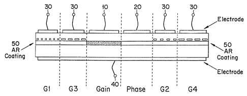
the present invention is illustrated in Figure 1. In Figure 1, note that a
gain
section which includes the light emitting layer of the substrate, is disposed
as
a center section of the laser. Next to the gain section is a phase control -
section. This section allows fine tuning of the lasing wavelength by
adjusting the round-trip phase of the light in the laser. This is accomplished
by changing the effective refractive index of the phase section through -
current injection. The phase control section can be omitted from the laser
when fine tuning of the wavelength is not necessary.
On either side of the gain section, a plurality of grating sections, G1,
G2, G3, and G4 are disposed. Although four grating sections are shown in
the exemplary embodiment of Figure 1, those skilled in the art will readily
appreciate that a greater or lesser number of gratings can be provided
~137~9~~
~..- _ 4
depending on the tuning range or ranges of the laser that are desired. This
feature of the present invention will become more apparent after reading the
following discussion. Also in Figure 1, note that the gain and phase sections
have electrical contacts 10 and 20, respectively, while each grating section
has its own electrical contact for current injection denoted by reference
number 30. A common ground contact 40 for all sections is also provided.
Additionally, each end of the laser device 50 is coated with an anti-
reflection
coating to avoid losing on the Fabry-Perot modes due to the end facets.
The periods (i.e., the center wavelengths) and the strengths (i.e., the .
coupling coefficients) for each of the grating sections G1 through G4 can be
selected so that when no current is applied to the gratings, there is no
spectral overlap between their reflection bands. In this way, there is no
feedback and thus no laser oscillation. The positioning of the grating
sections relative to the gain section 10 can be as follows. The grating
section with the longest center wavelength (smallest center frequency) is
denoted grating G1, the grating with the next longest center wavelength G2,
the grating with the third longest wavelength is G3 and the grating with the
shortest wavelength is G4. Then, the odd-numbered gratings are arranged
on one side of the gain section 10 and the even-numbered gratings are
arranged on the other side. This results in the arrangement of sections
illustrated in Figure 1. Although the exemplary embodiment of Figure 1
shows gratings Gl and G4 being further from the gain section than gratings
G3 and G2, respectively, those skilled in the art will appreciate that the
order of placement of the gratings on each side is not critical, the point
being to place the proper gratings on each side.
The spectral ordering of the grating sections G1-G4 is illustrated in
Figure 2. Note that although the reflection spectrums of the gratings are
illustrated in Figure 2 as being rectangular, those skilled in the art will
appreciate that the actual shape of the reflection spectrum is more complex.
However, rectangles are used in Figure 2 simply to illustrate that the
gratings are arranged in order of decreasing wavelength {increasing
~1~'~ ~9!~
~...- _
frequency). Thus, according to exemplary embodiments of the present
invention, gratings having decreasing periods are alternately placed on either
side of the gain section 10.
By injecting carriers via the electrodes 30 into the grating sections the
effective index of refraction, and thus the center wavelength of the
refraction
gratings, can be reduced. When the refractive index (n~) of a grating is
reduced there is a shift of the reflection band towards shorter wavelengths,
i.e., since the center wavelength ~=2n~A, where A is the physical period
of the grating. In this way, each grating can be tuned to make its own _.
reflection band coincide with the reflection band of a grating on the other
side of the gain section to provide lacing. Tuning of the lasing wavelength
can then be obtained by tuning both gratings involved and/or by using the
phase tuning section 20. Tuning both gratings, but in such a way that the
center wavelengths of their reflection bands are the same, allows tuning of
the lacing wavelength since lacing will occur only at wavelengths where
there is feedback (provided by the gratings). Within the range of frequencies
where the gratings provide feedback, the phase section can be used to fine-
tune the lacing wavelength. This is done by changing the effective refractive
index of the phase section by carrier injection. This index change will
change the round-trip phase of the light in the laser and thus the lacing
wavelength.
An example of a tuning operation according to the present invention
is illustrated in Figure 3. By applying currents to gratings G1 and G2 via
their respective electrode 30, the center wavelengths of Gl and G2 can be
moved to a desired position. The lacing wavelength can then be adjusted
using the phase section 20. Depending on the amount of tuning possible
with each grating, the lacing wavelength can be tuned continuously over the
complete range between two grating center wavelengths. Thus, for the
exemplary laser of Figure 1, three such continuous tuning ranges are created
as shown in Figure 4.
CA 02137596 2004-04-19
=~4-t9-04; 2:57PM; ;St43457929 # 4/ 4
6
Although the foregoing examples have been illustrated in terms of
gratings having center wavelengths which are equally spaced apart, those
skilled in the art will readily appreciate that gratings having unequal
spacing of
centered wavelengths can also be used to fabricate lasers in accordance with
S the present invention. Fox example, if it is desired to cover two wavelength
ranges that are relatively far apart, the arrangement illustrated in Figure 5
can
be used. Note that in Figure 5 that the center wavelengths of the two grating
sections having the shortest wavelengths, GI and G2, are closely grouped
together as are the two grating sections having the longest wavelengths, G3
and
G4. In this way two tuning ranges can be created, i.e., a range using GI and
G2 and a range using G3 and G4.
The structure of the gratings, gain and phase sections can be
implemented using conventional technology and, accordingly, are not further
described herein. For background material, however, reference is made to
1 S "Semiconductor Lasers for Coherent Optical Fiber Communications", T.L.
Koch and U. Korea, (J. Lightwave Technology, vol. $ (3) March 1990, pages
274 through 293). Lasers according to the present invention can be fabricated
using any semiconductor material which permits the fabrication of
heterostructure semiconductor lasersffor example, AIGaAs/GaAs and
InGaAsP/InP. The please and grating sections have a core (bulk or quantum
wells) such that the absorption edge of the core material has a shorter
wavelength than the light of the laser and a cladding with a larger bandgap.
The gain section has a material which can amplify the light going through when
current is injected therein
For the purposes of illustration, a specific example will now be
discussed. Assume that InGaAsP on a InP substrate is being used and that the
laser is to operate around 1.55p,.m (i.e., the wavelength of minimum loss in
optical fbers). Typical waveguide core dimensions for all sections are 0.6 to
2
microns wide and 0.1 to 0.5 microns thick. Using bulk material in the phase
and grating sections, the core material will typically have a bandgap in the
range of 1.3 to 1.42 microns. The latter is preferable
Amended Street
I I
'!ae 19/04/20D4 I~15:22 I~5143457929 [0 received
__._ .,...,...,~...,.... ~.f,~.___ .. _. a_,.. ,.._ _ _. _...
2~.37~~~
because a smaller bandgap energy (larger bandgap wavelength) gives larger
tuning ranges for the gratings. The tuning range of each grating for this
example will be about 7 to 12 nm.
The coupling coefficients K~ of the gratings, which measure grating
strength, should be large (i.e., about 100 cm'1 or more) to allow the use of
short grating sections. This is desirable for several reasons, for example, to
avoid stitching problems during a beam lithography, decrease absorption
losses, and decrease total cavity length to get better longitudinal mode
discrimination. On the other hand, the coupling coefficient should not be too_
large because the widih of the reflection band of a grating is proportional
thereto. If Li is the length of a grating, the maximum power reflectivity (at
the center wavelength) is approximately given by tanh2(K~L~. Taking a K~,
product of about 1 gives a reasonable peak reflectivity of about 0.58. For
K= 100 cm 1, this corresponds to a grating length of about 100 microns.
The phase section can be short (about 100 microns) and the gain section can
be between 300 and 500 microns long. The electrical isolation regions
between the sections should be on the order of 50 microns long. Thus, for
the device of Figure 1, the minimum length is on the order of 1.3 mm; a
relatively short length which beneficially increases fabrication yields.
As another example, assume that a laser according to the present
invention is to be used in a WDM (Wavelength Division Multiplexing)
system with 4 channel wavelengths. Channels 1 to 4 are at wavelengths of
1560, 1556, 1552 and 1548 nm, respectively (i.e., with a 4 nm spacing).
Also assume that the design objective is to reach all these channels with a
device which has a tuning range greater than 8 nm, K= 100 cm'1 and an
effective index n~. = 3.25 in the grating sections (this is a typical value;
the
exact value can be computed for each device). These design objectives
imply that the reflection bands will have a Full-Width Half Maximum
(hWI~ of about 2.4 nm. Thus, to avoid unwanted oscillation, the center
wavelengths of the gratings should be further apart than 2.4 nm, e.g., at
least 3 nm.
,~- . _ g 213' ~ 9 ~
An exemplary laser configuration according to the present invention
that achieves these objectives is a laser as illustrated in Figure 1, with
four
gratings having the following grating center wavelengths: 1564 nm (G1),
1560 nm (G2), 1552 nm (G3) and 1548 nm (G4). Given that the gratings
can be tuned at least 8 nm, all of the channel wavelengths can be reached as
follows: (1) by tuning G1 to coincide with G2, (2) by tuning both Gl and
G2 to 1556 nm, (3) by tuning G2 to coincide with G3, and (4) by tuning G3
to coincide with G4.
_ The above-described exemplary embodiments are intended to be
illustrative in all respects, rather than restrictive, of the present
invention.
Thus the present invention is capable of many variations in detailed
implementation that can be derived from the description contained herein by
a person skilled in the art. All such variations and modifications are
considered to be within the scope and spirit of the present invention as
defined by the following claims.