Note: Descriptions are shown in the official language in which they were submitted.
- 2137644
Servo Control Technique for an Optical Recording and
Reproducing System
The present invention relates generally to an optical
recording and reproducing system which optically records and
reproduces information onto and from an optical recording
medium such as an optical card or the like, and more
particularly to an improved servo control technique for for
the optical recording and reproducing system in which the
position of an objective lens provided in an optical head
for focusing light beam onto the information recording
surface of an optical recording medium is servo-controlled
to control tracking and focusing deviations of light spot on
the information recording surface.
Optical recording and reproducing systems are
conventionally known which record and reproduce information
onto and from a card-type optical recording medium (namely,
optical card) by moving the optical card relative to the
optical axis of optical energy such as a laser beam. With
the developments and wide spread of computers etc., wide
spread of optical cards have been highly expected in recent
years because they are portable and safe and provide a
relatively large storage capacity in spite of their small
2137~44
size, and so a variety of applications of the optical cards
have been contemplated, such as application as recording
media for patients' diagnosis in medical organizations.
A typical example of a known optical card is shown in
Figs. 4 and 5, of which Fig. 4 is a plan view of the known
optical card 11 and Fig. 5 shows a section "A" in enlarged
scale of the optical card 11 of Fig. 4. In these figures,
reference numeral 12 denotes a recording/reproducing area,
13 denotes guide tracks, and 14 denotes a data track. On
the recording/reproducing area is formed a recording layer
that is for example made of silver chloride photographic
material as base material. By irradiating laser light of
a suitable energy level from an optical head onto the
recording layer, an optical information unit called a "pit"
is formed in the data track 14. The irradiated position on
the recording layer of the laser light (laser light spot)
is varied by moving the optical card 11 relative to the
optical head in the X-axis direction (direction parallel to
the data and guide tracks of the optical card 11), so that
a series of pits can be formed in a desired arrangement
corresponding to desired digital information. Thus,
recording and reproduction of desired digital information
are performed by writing and reading the pit rows onto and
from the recording layer of the optical card 11.
In such a case, to form pit rows in the data track 14
of the optical card 11, an approach is generally employed
213764~
which uses a drive mechanism such as a linear motor to move
the optical card 11 relative to the optical head. However,
due to a limited operational accuracy of the drive
mechanism, the prior approach can not prevent occurrence of
mechanical position error, due to which pits can not be
formed accurately in the middle of the data track 14 located
between the guide tracks 13. This presents a significant
inconvenience that desired information can not be recorded
or reproduced accurately.
In order to prevent the above-mentioned inconvenience,
it is absolutely necessary to perform the pit recording and
reproduction with the light spot accurately positioned in
the middle between the two guide tracks 13. To this end,
automatic tracking control has been conventionally performed
in an attempt to compensate for any mechanical position
error caused.
This automatic tracking control is generally performed
on the basis of the so-called "three-beam method", in which
three laser beams spaced apart from each other by a
predetermined distance are irradiated from the optical head
in such a manner that the central laser beam corresponds in
to the data track 14 as a read/write beam and the two laser
beams on both sides of the central beam (side laser beams)
correspond to the guide tracks 13 on both sides of the data
track 14 as tracking beams. Namely, the three-beam method
measures the respective reflected lights of the two side
- 2137 644
laser beams from the optical card 11 so as to servo-control
the irradiated light spot positions in such a manner that
the tracking beams accurately correspond to the guide tracks
13 in predetermined positional relations and thus the
central read/write beam is allowed to be always accurately
positioned in a predetermined middle part of the data track
14.
Further, since it is necessary to constantly have
laser light beam(s) stably focused on the recording layer of
the optical card 11, automatic focusing control has also
been conventionally performed in the art.
The above-mentioned automatic tracking and focusing
control operations are respectively performed by minutely
driving the objective lens of the optical head, via
electromagnetic force applied via a tracking coil and a
focusing coil, in the Y-axis direction (i.e., direction
transverse to the data and guide tracks of the optical card
11) and in the Z-axis direction (i.e., direction
perpendicular to the recording/reproducing surface of the
optical card 11). The objective lens serves to focus the
laser beam irradiated from the optical head onto the
recording layer of the optical card 11 so as to form a
light spot (three light spots in the case of the above-
mentioned three-beam method) on the recording layer.
Figs. 6 and 7 show examples of the prior art servo
control systems used for the automatic tracking and focusing
- 2137644
control.
More specifically, Figs. 6 and 7 show examples of
conventional tracking control circuits 30a and 30b,
respectively, for performing the above-mentioned automatic
tracking control; Fig. 6 illustrates the basic arrangement
for the automatic tracking control, and Fig. 7 illustrates
an improved technique as disclosed in Japanese Patent
Publication No. HEI 5-47895.
First, the tracking control circuit 30a of Fig. 6 will
be described. A light detector 31 having a pair of light
receiving elements 31a and 31b disposed in a predetermined
arrangement is mounted within the optical head for
photoelectrically converting the reflection from the optical
card and input via the objective lens. The above-mentioned
two tracking beams of the reflection input to the light
detector 31 are received by the light receiving elements 31a
and 31b, respectively, so that received-light signals
responsive to possible tracking error are output from the
light receiving elements 31a and 31b. The output signals
from the light receiving elements 31a and 31b are then fed
to a differential amplifier 32 which in turn outputs a
difference signal between the fed signals and are also fed
to a summing amplifier 33 which in turn outputs a sum signal
of the fed signals. This sum signal is provided to a
division circuit 34 as a denominator signal A. The
difference signal is, on the other hand, provided to the
213~4~
division circuit 34 as a numerator and is divided by the sum
signal to be normalized.
For example, when the tracking light spots are
accurately positioned on the respective guide tracks 13 of
the optical card 11, the difference signal has a value of
zero or near zero, while the sum signal has a greatest
value. Accordingly, the output from the division circuit 34
has a value of zero or near zero, which indicates that the
laser light spots are located at a suitable position with
respect to the guide tracks 13.
When the tracking laser light spots are deviated from
the guide tracks 13, however, the difference signal has a
value greater or smaller than zero so that the output from
the division circuit 34 has a value greater than zero. In
this way, the division circuit 34 outputs a signal
corresponding to deviation amounts of the laser light spots
from the guide tracks 13 (i.e., tracking error). To provide
enhanced stability of the control loop, the output signal
from the division circuit 34 is subjected to "phase-
advancing compensation" by a phase compensation circuit 35.
The signal having undergone the phase-advancing compensation
is converted by a drive circuit 36 into electric current,
which is applied to a tracking coil 20 so as to drive the
objective lens in the Y-axis direction (direction transverse
to the data and guide tracks of the optical card 11).
Thus, the objective lens is driven in dependence on the
213~644
deviation amounts of the laser light spots from the guide
tracks 13.
The purpose of normalizing the difference signal by
means of the division circuit 34 as previously noted is to
keep constant the servo loop gain of the tracking control
circuit in order to guarantee accurate information recording
onto the optical card 11. For example, to comparatively
consider a possible variation between the amounts or power
levels of the laser light generated during the recording and
reproduction operations, the laser light power during the
recording is about 1.5 mW, which is about one hundred times
as large as the laser light power during the reproduction
of about 0.1 to 0.4 mW. Therefore, it is vitally important
to maintain a constant servo loop gain without being
influenced by such variation in the laser light amount.
The tracking control circuit 30b of Fig. 7 is designed
to maintain a constant servo loop gain of the tracking
control circuit without using the division circuit as shown
in Fig. 6. Light detection signals output from light
receiving elements 31a and 31b are fed to variable-gain
amplifiers 37a and 37b, which are constructed in such a
manner to stepwise switch their amplification factors in
response to instructions given from a control circuit 38.
Sample and hold circuits 39a and 39b sample and hold the
respective output signals from the variable-gain amplifiers
37a and 37b. Further, a subtraction circuit 40 performs
- 2137644
subtraction between the output signals of the sample and
hold circuits 39a and 39b to thereby provide a tracking
error signal. The tracking error signal provided from the
subtraction circuit 40 is subjected to phase-advancing
compensation by a phase compensation circuit 35 as in the
case of Fig. 6 and is applied to a drive circuit 36, which
in turn drives the tracking coil 20.
Fig. 8 is a signal timing chart explanatory of an
exemplary operation of the prior art technique as shown in
Fig. 7. Item (a) of Fig. 8 indicates signal representing
information to be recorded onto the optical card 11
(recording information signal), item (b) indicates
variations in the laser light power modulated by the
recording information signal, and item (c) indicates outputs
from the subtraction circuit 40. As shown in item (a) of
Fig. 8, the recording information signal varies between
values "1" and "0". In response to the variation in the
recording information signal, the generated laser light
power varies between levels "PL" and "PH" as shown in item
(b). A pit is formed in the optical card 11 when the
laser light power is at high level "PH", while no pit is
formed in the optical card 11 when the laser light power is
at low level "PL". Thus, the outputs of the light receiving
elements 31a and 31b vary in accordance with the variations
in the laser light power (between levels "PL" and "PH").
Here, in order to maintain a constant open-loop gain of the
- 2137644
tracking servo, the respective gains of the variable-gain
amplifiers 37a and 37b are changed. Additionally, in order
to eliminate discrepancies in the rise and/or fall of
signals in the servo loop which would be caused by sudden
changes in the light amount as shown in item (b), an
approach is taken in accordance with which signals in the
servo loop are sampled and held by the sample and hold
circuits 39a and 39b before the light amount change begins,
and the thus-held signals are released after the light
amount change.
However, the above-mentioned prior art arrangements
have the following shortcomings.
First, the Fig. 6 arrangement tends to be expensive
because it requires complicated analog processes using the
division circuit 34, and the arrangement is susceptible to
thermal drift due to the use of analog circuitry, thus
causing frequent tracking errors.
In contrast, the Fig. 7 arrangement provides a
solution to the problems of the above-mentioned Fig. 6
arrangement using the division circuit, by suitably changing
the gains of the variable-gain amplifiers 37a and 37b to
maintain a constant loop gain against the laser light power
variations. Nevertheless, this arrangement presents new
problems that the frequency response is poor due to the
necessity to change the gains of the variable-gain
amplifiers 37a and 37b, and the loop gain undesirably varies
- 2`1376~4
-- 10 --
because the reflection factors on the recording layer may
differ among different optical cards. Such conditions are
shown in item (c) of Fig. 8. Assuming that the gain for an
optical card of suitable reflectivity is Va, the gain for
an optical recording medium of higher reflectivity will
increase to Vb, and the gain for an optical recording medium
of lower reflectivity will decrease to Vc. Under such
conditions, accurate servo control can not be achieved and
tracking errors would result.
The automatic focusing control employs servo control
circuitry similar to the above-mentioned and hence would
encounter the same kinds of problems.
In recent years, an approach has been taken to
increase the recording density of optical cards in order to
provide increased storage capacity. In the light of such
increased density of optical cards, enhanced accuracy and
stability of the tracking and focusing control in particular
are highly demanded of the optical card recording and
reproducing devices. Therefore, it is extremely important
to overcome the above-mentioned problems.
It is therefore an object of the present invention to
provide an optical recording and reproducing system which is
capable of maintaining a constant servo loop gain without
being influenced by variation in the laser light amount or
difference in reflectivity characteristics of the recording
- 213~6~4
layers of optical recording media, to thereby permit
constantly stable tracking servo control and/or focusing
servo control by use of a relatively simple circuitry
structure.
In order to accomplish the above-mentioned object, the
present invention provides an optical recording and
reproducing system which records and reproduces information
onto and from an optical recording medium by irradiating
laser light generated from a laser light source onto the
optical recording medium, and which is provided with a servo
control section for detecting reflection of the laser light
from the recording medium to provide an error signal on the
basis of an amount of the detected reflection and
controlling formation of the laser light to be irradiated
onto the recording medium in response to the provided error
signal. In the recording and reproducing system in
accordance with novel features of the present invention, the
servo control section includes a switch section for
switching passage of the error signal, a smoothing section
for smoothing the error signal passed by the switch section,
and a controller section for monitoring the amount of the
detected reflection and controlling the switching action of
the switch setion based on the monitored amount, whereby a
gain of a servo loop in said servo control section is
controlled. The controller section may be designed to
control the switching action so that the gain of the servo
2137644
loop is maintained at a predetermined standard.
According to the principle of the present invention,
the servo control may be used for either tracking control
or focusing control, or for any other application as long
as similar servo control is performed (i.e., an error signal
is detected on the basis of the detected reflection amount
and formation of the laser light is servo-controlled in
response to the detected error signal) in the application.
The present invention is essentially characterized in
that, in the servo control section, there are provided the
switch section for switch-controlling the error signal, and
the smoothing section for smoothing the switch-controlled
error signal. The control section is further provided for
monitoring an amount of detected reflection from an optical
recording medium and controlling the switching action of the
switch section so as to control the loop gain of the servo
loop, e.g., to maintain it at a predetermined standard.
By thus monitoring the amount of the detected
reflection, in such a case where the laser light amount has
changed, or where the reflection amount has varied from a
predetermined standard, it is allowed to detect occurrence
of any factor causing variation in the servo loop gain. On
the basis of such monitoring, the switching action of the
switch section can be controlled in such a manner that the
loop gain is prevented from varying, i.e., that the loop
gain is maintained at the predetermined standard.
- 213764d~
- 13 -
For instance, a decrease in the detected reflection
amount from the predetermined standard will cause the loop
gain to be relatively decreased. Therefore, in this case,
the loop gain is controlled to be substantially maintained
at the predetermined standard by relatively increasing the
activation or conduction period of the switch section,
relatively increasing the level of the error signal smoothed
(integrated) by the smoothing section, and relatively
increasing the gain so as to compensate for the gain
decrease caused. Conversely, an increase in the detected
reflection amount from the predetermined standard will cause
the loop gain to be relatively increased. Therefore, in
this case, the loop gain is controlled to be substantially
maintained at the predetermined standard by relatively
decreasing the conduction period of the switch section
(i.e., deactivating the switch section), relatively
decreasing the level of the error signal smoothed
(integrated) by the smoothing section, and relatively
increasing the gain so as to compensate for the gain
increase caused.
Now, the preferred embodiment of the present invention
will be described in detail below with reference to the
accompanying drawings.
In the accompanying drawings:
Fig. 1 is a circuitry diagram showing examples of a
2137644
- 14 -
tracking control circuit and a focusing control circuit
employed in an optical recording and reproducing system in
accordance with an embodiment of the present invention;
Fig. 2 is a timing chart explanatory of the operation
of the embodiment of Fig. l;
Fig. 3 is a schematic perspective view showing an
structural example of an optical system of the optical
recording and reproducing system applicable to the present
invention;
Fig. 4 is a plan view showing an example of an optical
card applicable to the present invention;
Fig. 5 is an enlarged view of the optical card showing
a detailed example of its recording layer;
Fig. 6 is a circuit diagram showing an example of a
prior art tracking control circuit;
Fig. 7 is a circuit diagram showing another example of
a prior art tracking control circuit; and
Fig. 8 is a timing chart explanatory of the operation
of the tracking control circuit of Fig. 7.
Fig. 3 is a perspective view showing, by way of
example, a basic structure of an optical system of the
optical recording and reproducing system of the invention
which employs an optical card as a recording medium. Fig.
3 principally shows a relationship between the optical card
11 and the optical system of an optical head 2 located above
2137644
the optical card 11. The detailed structure of the optical
card 11 may be the same as shown in Figs. 4 and 5. By
means of an unillustrated drive means (e.g., a linear
motor), the optical card 11 is reciprocatingly movable in
the X-axis direction (direction parallel to guide and data
tracks 13 and 14 of the optical card 11).
In the optical head 2, a laser diode 27 is provided as
a laser light source, and diffused light generated from the
laser diode 27 is collimated through a collimating lens 26a.
The collimated laser light is then divided into three parts
through a diffraction grating 25 to form three laser light
beams as previously mentioned in connection with the
background of the invention. A beam splitter 24 serves to
separate the laser light irradiated onto the optical card 11
and reflected light (reflection) of the laser light from the
optical card 11. A reflecting mirror 23 serves to reflect
each of the laser light and reflected light to bend its
light path by 90 . Further, an objective lens 22 converges
and irradiates the collimated laser light onto a recording
layer of the optical card 11, to form a light spot thereon.
The reflected light separated by the beam splitter 24
is passed through a collimating lens 26b to be converted
into converged light. A concave lens 28 serves to convert
the converged light input from the collimating lens 26b into
suitable diffused light. An edge mirror 29 serves to divide
the reflected light from the optical card 11 equally into
2137~44
- 16 -
two parts. Light detectors 3 and 3', which receive the
respective light parts divided by the edge mirror 29,
convert the reflected light parts into electrical signals
for detection of tracking and focusing errors.
By electromagnetic force generated by a tracking coil
20, the objective lens 22 can be finely adjusted in position
in the Y-axis direction (direction transverse to the data
and guide tracks of the optical card 11), and by
electromagnetic force generated by a focusing coil 21, the
objective lens 22 can be finely adjusted in position in the
Z-axis direction (direction perpendicular to the
recording/reproducing surface of the optical card 11). The
tracking coil 20 is driven by signal output from the
tracking control circuit 41, while the focusing coil 21 is
driven by signal output from the focusing control circuit
42. Tracking and focusing errors are detected in an
arbitrary manner, and in response to the error detection,
the tracking control circuit 41 and the focusing control
circuit 42 servo-control the Y-axis and Z-axis positions of
the objective lens 22.
For detection of the tracking and focusing errors, the
so-called three-beam method and edge mirror method are
employed in the preferred embodiment.
To explain the three-beam method, laser light emitted
from the laser diode 27 is passed through the collimating
lens 26a and is divided by the diffraction grating 25 into
2137~44
- 17 -
three light parts to form three laser beams. The three
laser beams from the diffraction grating 25 are passed
through the beam splitter 24, reflecting mirror 23 and
objective lens 22, and then they are focused and irradiated
onto the recording layer of the optical card 11 to form
three light spots in predetermined positional relations to
each other. In the tracking servo control based on the
three-beam method, of the three divided laser light beams
focused onto the recording layer, the central laser beam is
positioned on the data track 14, and the other two or side
laser beams are positioned on the guide tracks 13 on both
sides of the data track 14.
The three laser beams focused onto the recording layer
of the optical card 11 in the above-mentioned manner are
reflected from the recording layer to become respective
reflections. One of the reflections which is from the data
track 14 (hereinafter referred to as a "first reflection")
is passed through the objective lens 22, reflecting mirror
23, beam splitter 24, collimating lens 26b, concave mirror
28 and edge mirror 29 and is then focused onto light
receiving elements 3a and 3'a of the light detectors 3, 3'.
The first reflection received by the light receiving
elements 3a, 3'a is photoelectrically converted into
electrical signals, which are then used as focusing signals.
Each of the central light receiving elements 3a, 3'a of the
light detector 3, 3' comprise at least two light receiving
- 213764~
- 18 -
element segments, so as to perform focusing control on the
basis of a balance state between the amounts of the
reflection received by the segments. In an alternative
arrangement, only the output from the light receiving
element 3a of one of the light detectors (for instance,
detector 3) may be used as such focusing signal.
On the other hand, the two reflections from the guide
tracks 13 on both sides of the data track 14 (hereinafter
referred to as "second reflections") are, similarly to the
first reflection, passed through the objective lens 22,
reflecting mirror 23, beam splitter 24, collimating lens
26b, concave mirror 28 and edge mirror 29 and are then
focused onto light receiving elements 3b, 3c and 3'b, 3'c
of the light detectors 3, 3'. The second reflections
received by the light receiving elements 3b, 3c and 3'b, 3'c
are photoelectrically converted into electrical signals,
which are then used as tracking signals. For example, in
each of the light detectors 3, 3', one of the light
receiving elements 3b or 3'b receives the reflection from
the left-side guide track 13, and the other light receiving
elements 3c or 3'c receives the reflection from the right-
side guide track 13. Since the tracking control is
performed on the basis of a balance state between the
received or detected amounts of the reflections from the
left-side and right-side guide tracks, only the output from
any pair of the left-side and right-side light receiving
2137644
-- 19 --
elements (e.g., 3b and 3c, 3'b and 3'c, 3b and 3'c, or, 3'b
and 3c) may be used as the tracking signals. But, the
total of the detected amounts of the reflections from the
left-side and right-side guide tracks 13 is constant, and
the difference between the detected amounts differentially
varies in such a manner that, as the detected light amount
in one of the light receiving elements increases due to a
deviation of the light spot positions, the detected light
amount in the other light receiving element decreases.
The edge mirror method is principally used as a
suitable method for detecting focusing errors, because it
provides better pull-in sensitivity as compared to the
conventional astigmatism method. Namely, the first
reflection, which is focused onto the light receiving
elements 3a and 3'a via the objective lens 22, reflecting
mirror 23, beam splitter 24, collimating lens 26b, concave
mirror 28 and edge mirror 29, assumes a suitable circular
cross-sectional shape when passing through the concave lens
28; however, the first reflection is divided into two light
parts of semicircular cross-sectional shape as it approaches
the edge portion of the edge mirror 29 disposed between the
concave lens 28 and the light detectors 3, 3'. One of the
divided semicircular light parts is passed through the edge
portion and is then focused onto one light receiving
elements 3a, while the other semicircular light part is
reflected from the edge mirror 29 and is then focused onto
- 2137644
- 20 -
the other light receiving element 4a. Focusing error is
detected on the basis of variation in the semicircular
luminous flux focused on the light receiving element 3a or
3'a. A focusing control circuit 42 performs automatic
focusing control by detecting a focusing error signal in
response to a focusing signal obtained on the basis of the
output signal of the light receiving element 3a or 3'a, and
applying driving current to the focusing coil 21 depending
on the detected error signal so that the objective lens 22
is driven in the Z-axis direction.
The tracking signals obtained by the light receiving
elements 3b and 3c or 3'b and 3'c of the light detector 3
and 3' are provided to a tracking control circuit 41 for
detection of tracking error. Thus, the tracking control
circuit 41 performs automatic tracking control by applying
driving current to the tracking coil 20 depending on the
detected tracking error so that the objective lens 22 is
driven in the Y-axis direction.
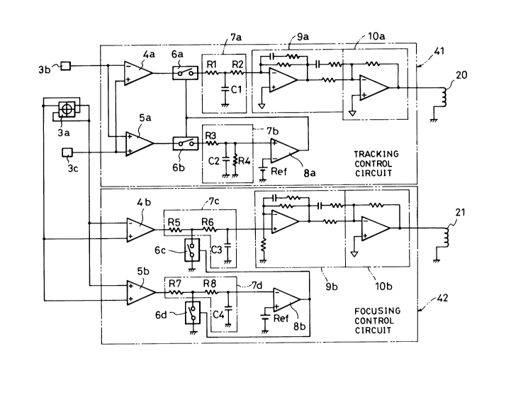
Next, with reference to Fig. 1, a description will be
given on preferred embodiments of the tracking and focusing
control circuits 41 and 42 in accordance with the present
invention.
To first describe the tracking control circuit 41, the
output signals of the light receiving elements 3b and 3c
that receive the reflections from the left and right guide
tracks 13 are both applied to a differential amplifier 4a
- 2137644
- 21 -
which in turn obtains a difference signal between the output
signals and also to a summing amplifier 5a which obtains a
sum signal of the output signals. As mentioned earlier, the
difference signal corresponds to a tracking error signal and
hence is called a tracking error signal. The sum signal
from the summing amplifier 5a corresponds to the detected
amount of the reflections and allows the total detected
amount of the reflections to be monitored. Namely, as
previously noted, the total detected amount, which should
normally be constant since the detected light amounts in the
tracking-oriented light receiving elements 3b and 3c are
differential to each other, tends to vary due to light
amount variation derived from variation in the laser light
power or due to difference in the reflective conditions of
individual optical cards. Therefore, as already known, the
difference signal needs to be normalized in dependence on
the variation in the sum signal. The present invention is
characterized by the provision of switch circuits 6a and 6b,
time constance circuits 7a and 7b and a comparator circuit
8a, as one exemplary arrangement for the required
normalization.
The above-mentioned difference and sum signals output
from the amplifiers 4a and 5a are fed to the switch circuits
6a and 6b, respectively. The switch circuit 6a passes the
output of the differential amplifier 4a to the time constant
circuit 7a in a switching fashion, while the switch circuit
213764~
- 22 -
6b passes the output of the summing amplifier 5a to the time
constant circuit 7b in a switching fashion. The time
constant circuit 7a comprised of resistors Rl and R2 and a
condenser C1 serves to average the output voltage signal
from the switch circuit 6a. Similarly, the time constant
circuit 7b comprised of resistors R3 and R4 and a condenser
C2 serves to average the output voltage signal from the
switch circuit 6b. These time constant circuits 7a and 7b
have a substantially same transfer function as expressed by
the following expression:
~Expression 1~
Transfer Function = {R2/(Rl+R2)} /(l+s-Tl)
= {R4/(R3+R4)} /(l+s-T2)
wherein
Tl = Rl-R2-Cl/(Rl+R2),
T2 = R3-R4-C2/(R3+R4), and
s is the result of subjecting y =~xdt to Laplace
transform.
The time constant circuit 7a is a kind of a smoothing
circuit or low-pass filter or integrating circuit which
operates with the above-mentioned transfer function and in
which a charging route is formed by the resistor Rl and
condenser C1 and a discharging route is formed by the
register R2 and a phase compensation circuit 9a provided at
the next stage to the resistor R2. The time constant
circuit 7b is a kind of a smoothing circuit or low-pass
21376~4
- 23 -
filter or integrating circuit which operates with the above-
mentioned transfer function and in which a charging route is
formed by the resistor R3 and condenser C2 and a discharging
route is formed by the register R4 connected to the earth.
The comparator circuit 8a compares the output signal
of the time constant circuit 7b which is applied to its "+"
input and represents the result of averaging or smoothing
the sum signal, and standard or reference voltage Ref
applied to its "-" input. The comparator circuit 8a
controls the switching action of the switch circuits 6a and
6b on the basis of the comparison result. More
specifically, the comparator circuit 8a activates (turns ON)
the switch circuits 6a and 6b when the output voltage of the
time constant circuit 7b is smaller than the reference
voltage Ref, but deactivates (turns OFF) the switch circuits
6a and 6b when the output voltage of the time constant
circuit 7b is greater than the reference voltage Ref. It
is a matter of course that each of switch circuits comprises
an electronically-switch-controlled switching gate element
such as a transistor.
The output signal of the time constant circuit 7a
which represents the result of averaging or smoothing the
difference signal is supplied to the phase compensation
circuit 9a where it is subjected to phase-advancing
compensation as mentioned earlier or phase-inversion
control. The resultant phase-controlled signal is passed to
- 2137644
- 24 -
a drive circuit 10a, which converts the signal into drive
current to be applied to the tracking coil 20. In response
to the drive current, the objective lens 22 is minutely
driven in the Y-axis direction.
Fig. 2 is a timing chart of various signals in the
principal sections of the Fig. 1 circuitry arrangement. In
Fig. 2, item (a) indicates information signal to be recorded
onto the optical card 11 (recording information signal),
item (b) indicates variation in the laser light power
modulated by the recording information signal, item (c)
indicates the output signal of the time constant circuit 7b,
and item (d) indicates the output signal of the comparator
circuit 8a.
An exemplary operation of the tracking control circuit
41 of Fig. 1 is explained as follows. In the case where
the relationship between the signal voltages input to the
comparator is that the output voltage of the time constant
circuit 7b is smaller than the reference voltage Ref, the
comparator circuit 8a performs control to turns ON the
switch circuits 6a and 6b. In response to this, the
difference signal from the differential amplifier 4a and the
sum signal from the summing amplifier 5a are fed to the time
constant circuits 7a and 7b, respectively, and the output
voltages of the circuits 7a and 7b increase with the lapse
of time. Thus, when the output signal of the time constant
circuit 7b gradually rises to become greater than the
-
2137644
reference voltage Ref, the comparator circuit 8a turns OFF
the switch circuits 6a and 6b. This causes the output
voltages of the time constant circuits 7a and 7b to fall
with time. In this manner, the ON/OFF action of the switch
circuits 6a and 6b is repeated in response to the rise/fall
of the output voltage of the time constant circuit 7b
relative to the reference voltage Ref. Here, a series of
the switching actions take place in proportion to the
detected-light-corresponding output voltages of the light
receiving elements 3b and 3c (i.e., total detection amount
of the reflection). In another words, faster switching
takes place as the detected-light-corresponding output
voltage becomes higher, while slower switching takes place
as the detected-light-corresponding output voltage becomes
lower. This allows the servo loop gain to be constantly
maintained at a suitable level.
Next, a description will be made on the focusing
control circuit 42 of Fig. 1.
The output from the central light receiving element 3a
in the light detector 3 is input to the focusing control
circuit 42. The light receiving element 3a is comprised of
at least two light receiving element segments, so as to
perform focusing control on the basis of a balance state
between the light amounts received in the these segments.
In the example of Fig. 1, the light receiving element 3a is
comprised of four adjoining light receiving element segments
213~644
- 26 -
arranged in a square shape, so as to obtain two pairs of
detected-light-corresponding output signals.
The servo control loop arrangement in the focusing
control circuit 42 is similar to the counterpart in the
above-mentioned tracking control circuit 41, and here a
difference between the two pairs of detected-light-
corresponding output signals is obtained by a differential
amplifier 4b, and a sum of the pairs of detected-light-
corresponding output signals is obtained by a summing
amplifier 5b. Further, for the same purposes as mentioned
above in connection with the tracking control circuit 41,
there are provided switch circuits 6c and 6d, time constant
circuits 7c and 7d and a comparator circuit 8b. Although
an example of the tracking control circuit 41 has been
described above in which the switch circuits 6a and 6b are
connected in series within the servo loop circuitry, an
example of the focusing control circuit 42 is shown here in
which the switch circuits 6c and 6d are connected in
parallel within the servo loop circuitry.
Namely, the difference signal output from the
differential amplifier 4b is passed to the time constant
circuit 7c which is comprised of resistors R5 and R6 and a
condenser C3, and the switch circuit 6c is connected between
the junction of the resistors R5 and R6 and the earth. The
sum signal output from the summing amplifier 5b is passed
to the time constant circuit 7d which is comprised of
2i37644
- 27 -
resistors R7 and R8 and a condenser C4, and the switch
circuit 6d is connected between the junction of the
resistors R7 and R8 and the earth. Similarly to the above-
mentioned time constant circuits 7a and 7b, the time
constant circuits 7c and 7d serve to average or smooth input
voltage and have a substantially same transfer function.
Further, similarly to the above-mentioned comparator
circuit 8a, the comparator circuit 8b compares the output
signal of the time constant circuit 7d corresponding to the
sum signal and standard or reference voltage Ref and
controls the ON/OFF state of the switch circuits 6c and 6d.
However, conversely to the above-mentioned, the comparator
circuit 8a deactivates or turns OFF the switch circuits 6c
and 6d when the output voltage of the time constant circuit
7d is smaller than the reference voltage Ref, and the
comparator circuit 8a activates or turns ON the switch
circuits 6c and 6d when the output voltage of the time
constant circuit 7d is greater than the reference voltage
Ref. This is because the switch circuits 6c and 6d are
connected in parallel with respect to the time constant
circuits 7c and 7d.
The output signal of the time constant circuit 7c
which represents the result of averaging the difference
signal is supplied to a phase compensation circuit 9b where
it is subjected to phase-advancing compensation as mentioned
earlier. The resultant phase-controlled signal is passed to
21~7644
- 28 -
a drive circuit lOb, which converts the signal into drive
current to be applied to the tracking coil 21. In response
to the drive current, the objective lens 22 is minutely
driven in the Z-axis direction.
An exemplary operation of the focusing control circuit
42 of Fig. 1 is explained as follows. In the case where
the relationship between the signal voltages input to the
comparator circuit 8b is that the output voltage of the time
constant circuit 7d is smaller than the reference voltage
Ref, the comparator circuit 8b performs control to turns OFF
the switch circuits 6c and 6d. In response to this, the
difference signal from the differential amplifier 4b and the
sum signal from the summing amplifier 5b are fed to the time
constant circuits 7c and 7d, respectively, and the output
voltages of the circuits 7c and 7d increase with the lapse
of time. Thus, when the output signal of the time constant
circuit 7d gradually rises to become greater than the
reference voltage Ref, the comparator circuit 8b turns ON
the switch circuits 6c and 6d. This causes the output
voltages of the time constant circuits 7c and 7d to fall
with time. In this manner, the ON/OFF action of the switch
circuits 6c and 6d is repeated in response to the rise/fall
of the output voltage of the time constant circuit 7d
relative to the reference voltage Ref. Here, a series of
the switching action take place in proportion to the
detected-light-corresponding output voltages of the light
21~76~4
- 29 -
receiving elements 3a. In another words, faster switching
takes place as the detected-light-corresponding output
voltage becomes higher, while slower switching takes place
as the light-detection-correspondent output voltage becomes
lower. This allows the servo loop gain to be constantly
maintained at a suitable level.
So far, the tracking control circuit 41 has been
described as including the switch circuits 6a and 6b
connected in series in the servo loop circuitry, and the
focusing control circuit 42 has been described as including
the switch circuits 6c and 6d connected in parallel in the
servo loop circuitry. However, the switch circuits 6a and
6b of the tracking control circuit 41 may be connected in
parallel, and the switch circuits 6c and 6d of the focusing
control circuit 42 may be connected in series.
Alternatively, both the switch circuits 6a and 6b of the
tracking control circuit 41, and the switch circuits 6c and
6d of the focusing control circuit 42 may be connected in
series or in parallel. In any event, it is a matter of
design choice whether the switch circuits 6a to 6d are
connected in series or in parallel in the servo loop
circuitry.
As apparent from the foregoing, the present invention
achieves the following advantageous results:
(1) Since the servo loop gain can be kept constant
irrespective of different reflectivities of the recording
2137644
- 30 -
layers of individual optical recording media, suitable servo
control such as for tracking or focusing control can be
constantly achieved without being influenced by the
different reflectivities.
(2) Since the same servo loop gain can be achieved for
both the recording and the reproduction, it is allowed to
perform servo control such as for tracking or focusing
control always in a suitable manner.
(3) Good frequency response can be provided.
(4) Since the optical recording and reproducing system
of the invention can be constructed of time constant and
switch circuits without requiring any expensive analog
division circuit, it is allowed to perform accurate tracking
and focusing control and thus enhance the recording and
reproducing accuracy with an inexpensive, simple circuit
structure.