Note: Descriptions are shown in the official language in which they were submitted.
2137721
- 1 - CFO 10396 ~
CA
ELECTRON SOURCE AND PRODUCTION THEREOF, AND
IMAGE-FORMING APPARATUS AND PRODUCTION THEREOF
BACKGROUND OF THE INVENTION
Field of the Invention
The present invention relates to an electron
source for emitting an electron beam and a process for
producing the electron source. The present invention
also relates to an image-forming apparatus such as an
image-displaying apparatus for forming an image on
irradiation of an electron beam.
Related Background Art
Two kinds of electron-emitting elements are
known: thermoelectron sources and cold cathode electron
sources. The cold cathode electron sources include
field emission type electron sources (hereinafter
referred to as "FE"), metal/insulator/metal type
electron sources (hereinafter referred to as "MIM"),
surface conduction electron-emitting elements, and the
like.
The above FE is exemplified by the ones
disclosed by W.P. Dyke & W.W. Dolan ("Field emission":
Advance in Electron Physics, 8, 89, (1956)), C.A:
Spindt ("Physical Properties of Thin-Film Field
Emission Cathodes with Molybdenum Cones": J. Appl.
Phys, 47, 5248, (1976)), etc.
The above MIM is exemplified by the ones
2137721
- 2 -
disclosed by C.A. Mead ("The Tunnel-Emission
Amplifier": J. Appl. Phys., 32, 646 (1961), etc.
The above surface conduction electron emitting
element is exemplified by the ones disclosed by M.I.
Elinson (Radio Eng. Electron Phys. 10, (1965)), etc.
The surface conduction electron-emitting
element utilizes the phenomenon that electrons are
emitted by flowing an electric current through a thin
film formed with a small area on a substrate and in
parallel to the surface of the film. Such surface
conduction electron-emitting elements include, in
addition to the above-mentioned one disclosed by
Elinson employing an SnOz thin film, the ones employing
an Au thin film [G. Ditter: "Thin Solid Films", 9,
317,(1972)], the ones employing Inz03/Sn02 thin film [M.
Hartwell and C.G. Fonstad: "IEEE Trans. ED Conf.", 519
(1975)], the ones employing a carbon thin film [H.
Araki et al.: Sinkuu (Vacuum), Vol. 26, No. 1, p. 22
(1983), and so forth.
Typically, the surface conduction electron-
emitting element has an element constitution as shown
in Fig. 23 disclosed by M. Hartwell as mentioned above.
In Fig. 23, the numeral 231 denotes a substrate, and
the numeral 232 denotes a thin film for electron-
emitting region formation (hereinafter referred to as
"emitting region-generating thin film") composed of a
thin metal oxide film or the like formed in an H-shaped
_2137721
- 3 -
pattern by a sputtering process. On the thin film 232,
an electron-emitting region 233 is formed by voltage
application called a "forming" treatment as described
later. The numeral 234 denotes a thin film having an
electron-emitting region.
In such surface conduction electron-emitting
elements generally, the electron-emitting region 233 is
formed by a voltage application treatment, i.e.,
forming, of an emitting region-generating thin film 232
prior to use for electron emission. The forming is a
treatment of flowing electric current by application of
voltage between the both ends of the emitting region-
generating thin film 232, thereby the emitting region-
generating thin film is locally destroyed, deformed, or
denatured to have high electric resistance to form the
electron-emitting region 233. The surface conduction
electron-emitting element having been subjected to the
forming treatment emits electrons from the electron-
emitting region on application of voltage to the thin
film 234 having the electron-emitting region 233.
Such conventional surface conduction electron-
emitting elements involve various problems in practical
uses. The inventors of the present invention, after
comprehensive investigations, have solved the practical
problems as described below.
For example, the inventors of the present
invention disclosed a novel surface conduction
2137721
- 4 -
electron-emitting element in which, as shown in Fig.
24, a fine particle film 244 is provided as the
emitting region-generating thin film between electrodes
(242, 243) on a substrate 241, and a fine particle film
244 is subjected to voltage application treatment to
form an electron-emitting region 245 (Japanese Patent
Application Laid-Open No. 2-56822).
In another example of electron sources, in
which a number of surface conduction electron-emitting
elements are arranged in lines, and the both ends of
the respective elements in each line are connected in
parallel by wiring (e. g., Japanese Patent Application
Laid-Open No. 1-283749 applied by the present
inventors).
In recent years, flat-panel display apparatuses
employing liquid crystal have become popular in place
of CRT as image-forming apparatus. However, the liquid
crystal, which does not emit light spontaneously,
requires back-light or the like disadvantageously.
Therefore, an emissive display device is demanded.
To meet such demands, an image-forming device
is disclosed in which an electron source having a
number of surface conduction electron-emitting elements
arranged therein is combined with a fluorescent
material which emits light on receiving electrons from
the electron source (e.g., USP 5,066,883 applied by the
present inventors). Such an image-forming device
_z1377zi
- 5 -
enables relatively easy production of apparatuses of
large picture area, and gives emissive display devices
with high image quality.
Display devices and other image-forming
apparatuses are necessarily expected to be larger in
the picture size, and finer in image quality. In the
above-mentioned electron sources having a number of
electron-emitting elements arranged therein frequently
encounter the problems as below:
1) Defectiveness or failure of the electron-emitting
element itself,
2) Disconnection in common wiring, or short circuit
between adjacent wiring, and
3) Insufficient insulation between layers at a cross-
over portion.
SUMMARY OF THE INVENTION
An object of the present invention is to
provide an electron source having a number of electron-
emitting elements arranged therein which is
substantially free from the above problems caused by
errors in the production process, in particular the
defects or failure of the electron-emitting element
itself, and to improve greatly the production yield of
electron sources and image-forming devices.
Another object of the present invention is to
provide an electron source and a process for producing
_2137721
- 6 -
the electron source, and also to provide an image-
forming device and production process thereof, which
are free from defect or failure of the electron-
emitting elements thereof and exhibiting extremely less
deterioration such as defective picture elements or
luminance variance, thus forming a high quality image.
A further object of the present invention is to
provide an electron source having a number of surface
conduction electron-emitting elements arranged therein
and an image-forming apparatus employing the electron
source, and to improve the production yield thereof and
to prevent the above deterioration of image quality,
thus forming a high quality image.
According to an aspect of the present
invention, there is provided an electron source
constituted of a substrate, and an electron-emitting
element provided on the substrate: said electron-
emitting element comprising a plurality of electrode
pairs having an electroconductive film between each of
the electrode pairs, and an electron-emitting region
being formed on the electroconductive film of selected
ones of the electrode pairs.
According to another aspect of the present
invention, there is provided an image-forming
apparatus, comprising the above electron source, an
image-forming member capable of forming an image by
irradiation of an electron beam emitted from the
2137721
electron source, and a modulation means for modulating
the electron beam irradiated to the image-forming
member corresponding to an inputted image signal.
According to still another aspect of the
present invention, there is provided an electron source
constituted of a substrate, and an electron-emitting
element provided thereon: said electron-emitting
element comprising a pair of element electrodes, a
third electrode placed between the pair of the element
electrodes, electroconductive films between the third
electrode and each of the pair of the element
electrodes; the electron-emitting region being provided
on a selected one of the electroconductive films.
According to a further aspect of the present
invention, there is provided an image-forming
apparatus, comprising the above electron source having
the third electrode, an image-forming member capable of
forming an image by irradiation of an electron beam
emitted from the electron source, and a modulation
means for modulating the electron beam irradiated to
the image-forming member corresponding to an inputted
image signal.
According to a still further aspect of the
present invention, there is provided a process for
producing an electron source having a substrate, and an
electron-emitting element provided on the substrate:
said process comprising steps of forming a plurality of
_213771
_8_
electrode pairs on the substrate, forming a thin film
for generating an electron-emitting region between each
of the electrode pairs, testing for detecting a defect
of the electrode pairs and/or the thin film, and
generating the electron-emitting region on the thin
film having no defect after the step of detecting a
defect.
According to a still further aspect of the
present invention, there is provided a process for
producing an electron source having a substrate, and an
electron-emitting element provided on the substrate:
said process comprising steps of forming a plurality of
electrode pairs on the substrate, forming a thin film
for electron-emitting region generation between each of
the electrode pairs, providing an electroconductive
member in the vicinity of the emitting region-
generating thin film, testing for detecting a defect of
the electrode pairs and/or the thin film, forming an
conductive path with the electroconductive member
between the electrode pair in the vicinity of any
defects of the thin film by heat-fusion of the
electroconductive member, and generating the electron-
emitting region on the thin film having no defect after
the step of detecting a defect.
BRIEF DESCRIPTION OF THE DRAWINGS
Fig. 1 is a perspective view of a part of a
_2137721
_ g _
display device of Embodiment 1 of the present
invention.
Figs. 2(a) to 2(e) are cross-sectional views
for explaining the process for producing the surface
conduction electron-emitting element of Embodiment 1.
Fig. 3 is a simplified circuit diagram for
explaining the step for testing the surface conduction
electron-emitting element of Embodiment 1.
Fig. 4 is a simplified circuit diagram for
explaining the process of forming of the surface
conduction electron-emitting element of Embodiment 1.
Fig. 5 is a drawing showing an example of
applied voltage waveforms for the forming.
Fig. 6 is a diagram showing an example of a
device for evaluating the characteristics of the
surface conduction electron-emitting element.
Fig. 7 is a diagram showing an example of a
typical characteristic curve of the element voltage
(Vf)-emitted current (Ie).
Fig. 8 is a simplified circuit diagram for
explaining a first driving method of the display device
of Embodiment 1 of the present invention.
Fig. 9 is a simplified circuit diagram for
explaining a second driving method of the display
device of Embodiment 1 of the present invention.
Fig. 10 is a simplified circuit diagram for
explaining a third driving method of the display device
_2137721
- 10 -
of Embodiment 1 of the present invention.
Fig. 11 is a plan view of the surface
conduction electron-emitting element of Embodiment 2 of
the present invention.
Fig. 12 is a flow chart for explaining
algorithm of the method of test of the surface
conduction electron-emitting element of Embodiment 2 of
the present invention.
Fig. 13 is a simplified circuit diagram for the
process of forming of the surface conduction electron-
emitting element of Embodiment 2 of the present
invention.
Fig. 14 is a simplified circuit diagram for
explaining the method of driving of the display device
of Embodiment 2 of the present invention.
Fig. 15 is a perspective view of the surface
conduction electron-emitting element of Embodiment 3 of
the present invention before forming treatment.
Figs. 16A(1) to 16A(6) and Figs. 16B(4') and
16H(4") are sectional views for explaining the process
of producing the surface conduction electron-emitting
element of Embodiment 3 of the present invention.
Fig. 17 is a partial perspective view of one
type of the display device of Embodiment 3 of the
present invention.
Fig. 18 is a simplified circuit diagram for
explaining the method of driving the display device of
2137721
- 11 -
Embodiment 3 of the present invention.
Fig. 19 is a partial perspective view of
another type of the display device of Embodiment 3 of
the present invention.
Fig. 20 is a plan view of a second surface
conduction electron-emitting element of Embodiment 3 of
the present invention.
Fig. 21 is a plan view of a third surface
conduction electron-emitting element of Embodiment 3 of
the present invention.
Figs. 22(1) to 22(6) are plan views showing
examples of defects and failure of a surface conduction
electron-emitting element.
Fig. 23 is a plan view of a conventional
surface conduction electron-emitting element.
Fig. 24 is a plan view of another conventional
surface conduction electron-emitting element.
DETAILED DESCRIPTION OF PREFERRED EMBODIMENT
The problems caused by errors in producing an
electron source having arrangement of a number of
electron-emitting elements and image forming device
employing the electron source are as below:
a) Electrical short circuit (failure)
b) Electrical disconnection (failure)
c) Faulty characteristics in electron emission
(defectiveness)
2137?21
- 12 -
The above defectiveness and failure are
comprehensively investigated by the inventors of the
present invention. As the results, the interesting
information as described below has been obtained
regarding the electron-emitting element, in particular,
the surface conduction electron-emitting element. It
is explained by reference to Figs. 22(1) to 22 (6).
Figs. 22(1) to 22(6) are plan views of
substrates having a surface conduction electron-
emitting element thereon before the forming treatment
for electron-emitting region formation.
The electrical short circuit in the surface
conduction electron-emitting element is caused by
bridging between element electrodes 225, 226 by an
electroconductive substance as shown in Fig. 22(1).
Such bridging naturally makes infeasible the effective
voltage application to the emitting region-generating
thin film 224, whereby the forming treatment (namely,
electric current flowing treatment of the emitting
region-generating thin film 224) or driving is made
impracticable. In some cases, such electrical short
circuit causes over-current, thereby a driving circuit
is broken.
The aforementioned bridging results mainly from
imperfect etching caused by sticking of dust on the
photoresist or by local irregularity of the etchant on
photolithographic formation of element electrodes 225,
2137721
- 13 -
226, or otherwise, in the case of formation of the
electrode pattern by a lift-off method, the bridging is
caused by a peeled fraction formed by imperfect washing
after the lifting-off and lying between the element
electrodes 225, 226.
The electrical disconnection in the surface
conduction electron-emitting element is caused by
disconnection of the emitting region-generating thin
film 224 at any point between the formed element
electrodes 225, 226 as shown in Figs. 22(2) and 22(3).
Such disconnection naturally makes impracticable the
effective application of voltage to the emitting
region-generating thin film 224, and renders
impracticable the aforementioned forming treatment and
practical driving.
The electrical disconnection shown in Fig.
22(2) occurs in most cases is caused by positional
deviation of a mask pattern during formation of the
emitting region-generating thin film 224 or by partial
exfoliation of the thin film 224 after its formation.
The electrical disconnection shown in Fig.
22(3) is caused in most cases by a defect of the formed
film of element electrodes 225, 226, or by partial
exfoliation of the emitting region-generating thin film
224 after its formation.
The faulty electron-emission characteristics in
the surface conduction electron-emitting element is
_2137721
- 14 -
caused by incomplete short-circuiting or incomplete
disconnection as shown in Figs. 22(4) to 22(6). With
such faulty characteristics, the voltage is not
effectively applied to the emitting region-generating
thin film 224, or the electric field or the electric
energy deviates from the designed value, whereby the
forming treatment or the voltage application in driving
cannot be conducted as designed, and the emitted
current (outputted electron beam) remarkably decreases.
The present invention is made on the basis of
the above findings. The preferred embodiments of the
present invention are described below in detail.
In a first feature of the present invention, a
plurality of emitting region-generating thin films are
provided on an electron-emitting element in case of
occurrence of defectiveness or failure in the electron-
emitting element.
According to the present invention, an
electron-emitting region can be formed by use of a
remaining normal emitting region-generating thin film
even when defectiveness or failure arises in some of
the plurality of the emitting region-generating thin
films.
The plurality of emitting region-generating
thin films are preferably formed between the element
electrodes electrically in series or in parallel as
described later.
213'~~~:1
- 15 -
When defectiveness or failure arises in an
emitting region-generating thin film, that failing or
defective thin film is not subjected to the forming
treatment, and effective driving signal is not applied
to the failing or defective thin film.
In a second feature of the present invention, a
means for switching electrical connection of the
emitting region-generating thin films.
An example of the means for switching
electrical connection is a selecting electrode provided
on the electron-emitting element for selectively
switching the electron-emitting regions. In utilizing
the selecting electrode, satisfactory electron-emitting
regions (or conversely defective or failing electron-
emitting regions) are memorized preliminarily in a
memory, and according to the information read out from
the memory, the driving signal is selectively applied
to the selecting electrode and the element electrode.
Another example of the means for switching
electrical connection is a heat-fusible
electroconductive member provided in proximity to each
of the electron-emitting region, which is heated at the
section where the electric connection is to be
switched. With this heat-fusible member, a new
electroconductive path is formed so that voltage may
not be applied practically to the electron-emitting
region exhibiting failure or defectiveness. For
_213~72~,
- 16 -
selective heating, for example, an infrared laser beam
is irradiated selectively to a desired spot.
The means for switching electrical connection,
according to the present invention, enables electrical
forming treatment selectively of thin films which
exhibit neither defectiveness nor failure.
Additionally, driving signals are applied selectively
to normal electron-emitting region, thereby undesirable
excessive power consumption and over-current are
prevented at the emitting region-generating thin films
exhibiting failure or defectiveness.
In a third feature of the present invention,
when defectiveness or failure arises in any of the
plurality of electron-emitting regions of the electron-
emitting element, the electrical conditions for driving
the normal electron-emitting regions are corrected
corresponding to the number of the defective or failing
electron-emitting regions. The correction of the
electrical conditions for driving is conducted by
adjusting the driving voltage, or length or number of
the driving pulses applied to the electron-emitting
element.
The driving voltage is adjusted in
correspondence with the electron emission
characteristics of each normal electron-emitting
element with reference to the voltage applied to the
electron-emitting region of the element.
213772.
- 17 -
The adjustment of the length or number of the
driving pulse is conducted by increasing it
approximately in proportion to the ratio of (number of
electron-emitting regions in one electron-emitting
element)/(number of normal electron-emitting regions in
the element).
By the adjustment of the driving conditions of
the electron-emitting element exhibiting defectiveness
or failure, an electron beam output with normal
intensity and a normal charge quantity can be obtained
at approximately the same level as the normal electron-
emitting element according to the present invention.
The above means may be practiced solely or in
combination of two or more thereof. The present
invention is suitably applicable particularly to
surface conduction electron-emitting elements.
The electron-emitting region on the thin film
is constituted of electroconductive fine particles of
0
several ten A in diameter, and other portion of the
thin film is constituted of a fine particle film which
is a film formed from fine particles. The fine
structure of the fine particle film includes dispersion
of individual separate particles, and aggregation
(planar or spherical) of fine particles (including an
island pattern). The thin film having an electron-
emitting region may be a carbon film on which
electroconductive fine particles are dispersed.
213 7'21
- 18 -
The material for constructing the thin film
having an electron-emitting region is exemplified by
metals such as Pd, Ru, Ag, Au, Ti, In, Cu, Cr, Fe, Zn,
Sn, Ta, W, Nb, Mo, Rh, Hf, Re, Ir, Pt, Al, Co, Ni, Cs,
Ba, and Pb; oxides such as PdO, SnOZ, In203, PbO, and
Sbz03; borides such as HfH2, ZrBz, LaBb, CeBb, YH4, and
GdB4; carbides such as TiC, ZrC, HfC, TaC, SiC, and WC;
nitrides such as TiN, ZrN, and HfN; semiconductors such
as Si, and Ge; carbon, and the like.
The thin film having an electron-emitting
region is formed by vacuum vapor deposition,
sputtering, chemical vapor phase deposition, dispersion
coating, dipping, spinner coating, or a like method.
Embodiment 1
Embodiment 1 of the present invention is
described by reference to Figs. 1 to 10.
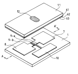
Fig. 1 is a perspective view of a portion of a
display device of the present invention, showing one of
surface conduction emitting elements as an electron
source and a face plate comprising a fluorescent
substance as an image-forming member. The surface
conduction emitting element in Fig. 1 is constructed of
an insulating substrate 1, (e. g., made of glass),
electrodes 7,8, thin films 9-a, 9-b, for electron-
emitting region formation (electron-emitting region
formed in 9-b), and a selecting electrode 10. The face
plate 11 of the display device is constructed of a
2137721
- 19 -
light-transmissive plate 61 (e. g., made of glass),
having on the inside face thereof a metal back 63 and
a fluorescent material 62 generally known for CRT use.
Further, under the fluorescent material 62, a light-
s transmissive electrode, (e. g., made of an ITO thin
film) may be provided which are known in the
application field of CRT. A voltage (e.g., 10 KV) is
applied to the metal back 63 (or the light-
transmissive electrode) from a high voltage power
source not shown in the drawing. When an electron beam
is emitted from the surface conduction emitting
element, a portion of the fluorescent material is
illuminated by the electron beam to emit visible light.
The face plate also constitutes a portion of a vacuum
envelope (not shown in the drawing). The interior of
the envelope is maintained at a vacuum (e.g., 10-6
Torr).
The surface conduction emitting element of this
Embodiment is prepared in a manner as follows, for
example. Figs. 2(a) to 2(e) illustrate sectional views
taken along line A-A' of the substrate shown in Fig. 1
to explain the production process. Figs. 2(a) to 2(e)
are drawn in an arbitrary size scale for convenience of
illustration.
(Step a) On a soda lime glass substrate 1
having been washed sufficiently with pure water, a
surfactant, and an organic solvent, is formed a pattern
2137721
- 20 -
41 for element electrodes 7, 8 and a selecting
electrode 10 with a photoresist (RD-2000N-41, made by
Hitachi Chemical Co., Ltd.), and thereon a Ti layer 45
0
of 50 A thick, and an Ni layer 44 of 1000 A thick are
laminated successively by vacuum vapor deposition.
(Step b) The photoresist pattern 41 is
dissolved off with an organic solvent, and a part of
the Ni/Ti deposition film 44/45 is lifted off to form
element electrodes 7, 8 and a selecting electrode 10
constructed of Ni/Ti. The gaps G between the element
electrode 7, 8 and the selecting electrode are 2
microns, for example.
(Step c) A mask pattern 42 is formed by
deposition of a Cr film of 100 A thick by vacuum vapor
deposition for formation of an emitting region-
generating thin film.
(Step d) On the above substrate 1, an organic
Pd solution (CCP 4230, made by Okuno Seiyaku K.K.) is
applied while the substrate 1 is being turned by use of
a spinner, and the applied matter is baked to form a
thin film 43 composed of fine Pd particles.
(Step e) The thin film 43 and the Cr
deposition film 42 are lifted off by wet etching with
an acid etchant to form emitting region-generating thin
films 9-a, 9-b.
The production process of the element
electrodes 7, 8, a selective electrode 10, and thin
217721
- 21 -
films 9-a, 9-b are described above. The produced
electron-emitting element substrate is tested for
defectiveness or failure.
In a first example of the test method, an
abnormal shape of the element electrodes 7, 8, the
selecting electrode 10, or the thin film 9-a, 9-b for
electron-emitting region formation is detected by use
of combination of an image pickup apparatus like an
industrial TV camera having a magnifying lens with an
image processor. That is, the image on the upper face
of the face plate is taken by an image pickup apparatus
and the image data is once stored in an image memory,
and the memorized image data is compared by pattern
matching with another image data having preliminarily
been memorized of a normal substrate. When the both
image data coincide with each other, the substrate is
evaluated as being normal. The defects and failure
shown in Figs. 22(1) to 22(6) are detectable in most
cases with this test method. The evaluation results
for respective electron-emitting region are stored in a
test result memory mentioned later.
In a second example of the test method, an
abnormal state is detected by measuring the electric
resistance, namely a current intensity flowing a test
sample on application of a predetermined voltage. Fig.
3 is a simplified block diagram of a circuit for
explaining this test method. The circuit for detection
2137721
- 22 -
of Fig. 3 comprises a current-measuring circuit 51, a
constant voltage power source 52, a change-over switch
53, a controlling CPU 54, a measured data storing
memory 55, comparison-evaluation circuit 56, a ROM 57
(read-only memory) in which normal current value is
memorized preliminarily, and an evaluation result
storing memory 58.
The current-measuring circuit 51 has
sufficiently low impedance and is used for measuring
the electric current flowing through a test sample on
application of the output voltage of the constant
voltage source 52, and outputs the measured data to the
measured data storing memory 55. The constant voltage
source 52 generates a voltage at such a level that the
test sample is not deteriorated by the current flowing
through the sample. The constant voltage source 52 has
a current limiter since some sample may have extremely
low voltage, like a sample having a short-circuit
defect. The change-over switch 53 is used for
switching the test sample, and may be a mechanical
switch or a semiconductor like a transistor. Fig. 3
shows an example of the measurement of the electric
resistance of the 9-b side of the emitting region-
generating thin film. The resistance of the 9-a side
can be measured by reversing the connection of the
change-over switch 53.
In Fig. 3, control signal from the CPU 54 is
_2137721
- 23 -
not shown for simplification of the drawing. The
controlling CPU 54 controls operation of the current
measuring circuit 51, the constant voltage source 52,
the change-over switch 53, the measured data storing
memory 55, the comparison-evaluation memory 56, the ROM
57, and the evaluation result-storing memory 58.
Under the control by the controlling CPU, the
test is conducted, for example, in the steps as
follows. Firstly, the CPU 54 sends a control signal to
the change-over switch 53 to select the "a" side. Then
the CPU 54 sends a control signal to the constant
voltage source 52 to output the measurement voltage.
Further, the CPU 54 outputs control signals suitably to
the measuring circuit 51 to measure the current
intensity and write the measured data into the measured
data storing memory 55. By the above operation, the
current flowing from the element electrode 7 through
the emitting region-generating thin film 9-a to the
selecting electrode 10, and the measured data is
written in the measured data storing memory 55. Then a
control signal is sent to the constant voltage source
52 to stop the measuring voltage output, and a control
signal is sent to the change-over switch 53 to change
the connection from the "a" side to the "b" side.
Thereafter in the same manner as above, the intensity
of the current flowing between the element electrode 8
and the selecting electrode 10, and the measured data
2137721
- 24 -
is written in the data storing memory 55.
The CPU 54 send a control signal respectively
to measured data storing memory 55 and ROM 57 to output
the stored data to the comparison-evaluation circuit
56. Thereby, the measured data is inputted from the
measured data storage memory 55, and the current
intensity value of a normal test sample is inputted
from the ROM 57, to the comparison-evaluation circuit
56. The comparison-evaluation circuit 56 compares the
above two current values and judges whether the
measured data is normal or not. Generally, the current
intensity value of the test sample varies to some
extent even with a normal sample not showing
defectiveness nor failure described in Figs. 22(1) to
22(6). The ROM 57 memorizes the mean value of the
variation. The comparison-evaluation circuit 56 judges
the occurrence of failure as shown in Figs. 22(5) to
22(6) if the measured value is in the range of from
1/100 times to 1/2 times the value read out from the
ROM 57; judges the occurrence of failure as shown in
Fig. 22(4) if the measured value is in the range of
from 3/2 times to 10 times the value; and judges the
occurrence of failure as shown in Fig. 22(1) if the
measured value is 10 times the value. Naturally, the
evaluation criteria are shown only as an example, and
the current value for the evaluation may be varies in
accordance with the nature of the defectiveness and
_2137721
- 25 -
failure. Furthermore, the comparison and evaluation
may be made by reference to the upper limit and the
lower limit memorized by the ROM 57.
The evaluation results are stored in the data
storing memory 55. By the above-mentioned procedure,
defectiveness and failure are detected electrically.
According to the above test results, the
emitting region-generating thin film is subjected to
electric forming treatment, which is explained by
reference to Fig. 4. The circuit for forming treatment
of Fig. 4 comprises a forming power source 61, a
change-over switch 53 similar to the one explained in
Fig. 3, a controlling CPU 64, and a evaluation result
storing memory 68. The evaluation result storing
memory 68 has preliminarily memorized the test results
obtained optically or electrically as mentioned above.
The controlling CPU 64 controls suitably the operation
of the forming power source 61, the change-over switch
53, and the evaluation result storing memory 68.
Firstly, the control CPU 64 reads out the test
results from the evaluation result storing memory 68.
The test results include three cases: a first case in
which both the 9-a side and the 9-b side of the
emitting region-generating thin film are normal, a
second case in which one of the 9-a side and the 9-b
side of the thin film only is normal, and a third case
in which both the 9-a side and the 9-b side are
213721
- 26 -
abnormal.
In the above first case in which both sides of
the emitting region-generating thin film are normal,
one of the two thin films is treated for electric
forming. In this Embodiment, the controlling CPU 64
sends a signal to the change-over switch to select and
connect the "a" side. Then the controlling CPU 64 send
a signal to the forming power source 61 to output the
predetermined forming voltage. An example of the
predetermined forming voltage is shown in Fig. 5. In
this example, the forming voltage is applied as
triangular pulses with T1 of 1 msec, Tz of 10 msec, and
the peak voltage of 5 V, for 60 seconds under a vacuum
of 10'6 Torr. Thereby an electron-emitting region is
formed on a portion 9-a of the emitting region-
generating thin film. The electron-emitting region
comprises dispersed fine particles mainly composed of
palladium, the fine particles having an average
0
diameter of 30 A. The forming voltage is not limited
to the one in the above waveform but may be in any
other waveform such as a rectangular wave. The wave
height, the pulse width, and the pulse interval are not
limited to the above values provided that the electron-
emitting region is formed satisfactorily.
In the case where only one of the emitting
region-generating thin films is in a normal state, the
controlling CPU 64 sends a control signal to the
2137721
- 27 -
change-over switch 53 to connect the normal side of the
emitting region-generating thin film. Fig. 4 shows an
example in which the portion 9-b of the thin film is
normal and is connected. The electrical forming
treatment is conducted as described above to form an
electron-emitting region on the emitting region-
generating thin film.
In extremely rare case where the both portions
of the emitting region-generating thin film are
abnormal, the controlling CPU 64 does not output a
signal to conduct the forming treatment. If the
defects or the failing points are repairable, the
emitting region-generating thin films is repaired and
tested again. If the repair is difficult, the
materials are reused desirably as the starting
materials.
The electric circuit for testing shown in Fig.
3 and the electric circuit for forming treatment shown
in Fig. 4 resemble each other in construction.
Therefore, the both circuit can be unified into one
circuit. In the unification, the circuit construction
of Fig. 3 is employed basically, and the current-
measuring circuit 51 is designed to have sufficiently
low impedance so as not to cause difficulty in forming
treatment, and further the constant voltage power
source 52 is replaced by another power source which is
capable of outputting both the constant voltage for
2137721
- 28 -
measurement and the pulse voltage for the forming
treatment. Naturally the controlling CPU 54 serves for
control-programming of testing as well as for control-
programming of forming treatment.
As described above, an electron-emitting region
has been formed selectively only on the normal one of
the two emitting region-generating thin films. The
output characteristics of the obtained surface
conduction emitting element are described, and further
the driving method of the surface conduction emitting
element for use for image-forming apparatus is
explained.
Fig. 6 illustrates roughly a measurement-
evaluation device for measuring the output
characteristics. The device comprises a power source
71 for applying an element voltage (voltage applied to
the element) Vf to the surface conduction emitting
element, an anode electrode 72 for capturing emission
current Ie emitted from the surface conduction emitting
element, a high voltage power source 73 for applying
voltage to the anode electrode 72, and an ammeter 74
for measuring the emission current. The electron-
emitting element and the anode 72 are placed in a
vacuum chamber equipped with tools such as vacuum pump
and a manometer necessary for a vacuum apparatus (not
shown in the drawing) so that the desired measurement
and evaluation can be conducted under vacuum. The
.137721
- 29 -
measurement can be conducted at an anode voltage
applied by the high voltage power source 73 in the
range of from 1 KV to 10 KV, and at the distance
between the anode electrode and the electron-emitting
element in the range of from 3 mm to 8 mm. Fig. 6
shows, as an example, measurement of electron emission
from the electron-emitting region 3 at the 9-b side
between the selecting electrode 10 and the element
electrode 8 on one of the two emitting region-
generating thin films on the surface conduction
electron-emitting element. In order to evaluate the 9-
a side, the power source 71 is connected between the
selecting electrode 10 and the element electrode 7 (not
shown in the drawing).
Fig. 7 shows a typical Ie-Vf characteristics of
a normal surface conduction electron-emitting element
as measured with the above measurement-evaluation
apparatus. The characteristic curve is shown in
arbitrary units since the absolute value of the output
characteristics depends on the size and the shape of
the electron-emitting element, etc. As is clear in
Fig. 7, the three characteristics are included in the
relation between the element voltage Vf and the
emission current Ie in a normal surface conduction
electron-emitting element.
Firstly, in this element, the emission current
Ie increases rapidly by application of voltage higher
213772?
- 30 -
than a certain voltage (a threshold voltage, shown by
Vth in Fig. 8), and the emission voltage Ie is nearly
zero at the voltage lower than the threshold voltage.
Thus, the element is a non-linear element having a
definite threshold voltage Vth to the emission current
Ie.
Secondary, the emission current is controllable
by the element voltage Vf because of dependence of the
emission current Ie on the element voltage Vf.
Thirdly, the quantity of electric charge of the
emitted electrons captured by the anode electrode 72
depends on the time of application of the element
voltage Vf. Therefore, the quantity of the electric
charge captured by the anode electrode 72 is
controllable by the time of application of element
voltage Vf.
In applying the element to an image-forming
apparatus by utilizing the above characteristics,
electrons are made to be emitted by application of an
element voltage higher than Vth in accordance with the
image to be formed, and the element voltage Vf or the
voltage application time is controlled in accordance
with the density of the image. Three examples are
explained by reference to Figs. 8 to 10, which show
circuit constitution for driving the element in
accordance with inputted image signals in a display
unit of Fig. 1 employing a surface conduction electron-
2137721
- 31 -
emitting element having been suitably treated for
forming in a method shown in Fig. 4. In these
examples, the normal electron-emitting region a.s formed
on the 9-b side of the emitting region-generating thin
film.
In Fig. 8, the numerals 90 and 91 denote a
voltage source for generating a voltage Vd which is
higher than Vth of the surface conduction electron-
emitting element; the numeral 92 denotes a pulse width
modulation circuit; 93 a change-over switch; 94, a
controlling CPU; and 68, an evaluation result storage
memory. In the example of Fig. 8, the element
electrodes 7, 8 are electrically connected respectively
to output voltage Vd of the voltage source 90 and a
ground level. To the selecting electrode 10 of the
surface conduction electron-emitting element, driving
signals are given to drive selectively the normal
electron-emitting region in accordance with the image
signals from the outside. That is, the controlling CPU
94 sends control signals to the change-over switch 93
in accordance with the evaluation results read out form
the evaluation result storing memory 68, whereby the
driving voltage is selected for driving the normal
electron-emitting region. For example, in this
example, the terminal "b" of the change-over switch is
made to be connected to the circuit to select the
output voltage Vd of the voltage source 91. (When the
2z377zz
- 32 -
normal electron-emitting region is formed on the 9-a
side of the emitting region-generating thin film, the
terminal "a" is connected to select the ground level.)
The pulse width modulation circuit 92 modulates
the driving voltage selected by the change-over switch
into a pulse voltage having width corresponding to the
image signal given from the outside, and gives the
modulated voltage to the selecting electrode 10. By
this modulation, a pulse of longer duration is applied
to the selecting electrode 10 for higher level of
luminance of the image signal.
In this example, as describe above, it is
practicable to emit electrons only from the normal
electron-emitting region by applying a different fixed
potential to the element electrodes 7 and 8
respectively and applying selectively, to the selecting
electrode 10, a potential equal to the one of the above
different fixed potentials. In such a manner,
disadvantages of unnecessary power consumption or over-
current can be caused since an effective voltage is not
applied because of no voltage difference between the
both ends of the defective or failing emitting region-
generating thin film. Thus an image display having
excellent gradation is obtainable by modulating the
driving pulse width of the driving voltage applied to
the selecting electrode in accordance with the external
image signal. The voltage sources 90 and 91 for
2137721
- 33 -
generating the constant voltage Vd may be unified into
one power source.
Another driving method is described by
reference to Fig. 9. In Fig. 9, the numeral 101
denotes a voltage source which generates a voltage Vd
higher than Vth of the surface conduction electron-
emitting element; 102, a pulse width modulation
circuit; 103, a change-over switch; 104, a controlling
CPU; and 68, an evaluation result storing memory. In
the driving method of the surface conduction electron-
emitting element in this example, a fixed potential
(ground level) is applied to the selecting electrode
10. A driving signal which is modified in pulse width
in accordance with the image signal from the outside is
selectively applied only to a normal electron-emitting
region side. That is, the controlling CPU 104 send a
signal to the change-over switch 103 according to the
evaluation result read out from the evaluation result
storing memory 68, whereby the element electrode at the
normal electron-emitting region side only is
selectively connected to the voltage source 101 and the
pulse width modulation circuit 102. In Figs. 2(a) to
2(e), for example, the terminal "b" of the change-over
switch 103 is connected, and the driving signal is
applied to the electron-emitting region 3 on the 9-b
side of the emitting region-generating thin film the
driving signal applied to the electron-emitting region
zi377z1
- 34 -
3 is a pulse voltage signal having a wave height Vd of
the voltage source 101 and having a pulse width which
has been modified by the pulse width modulation circuit
102 in accordance with the image signal from the
outside. A pulse of a larger time width is applied to
the electron-emitting region 3 for a higher luminance
level of the image signal.
In this example, as described above, it is
practicable to emit electrons from only the normal
electron-emitting region by applying a fixed potential
(ground level) to the selecting electrode 10 and
applying a driving signal selectively to the element
electrode of the normal electron-emitting region side.
In this method, since no current path is formed in the
defective or failed emitting region-generating thin
film, disadvantages of unnecessary power consumption,
over-current, etc. are not caused. Further in this
example, image display with high gradation is
practicable by modification of the pulse width of the
driving signal applied to the element electrode in
accordance with the image signal inputted from the
outside.
A still another example of the method of
driving the element is described by reference to Fig.
10. In Fig. 10, the numeral 110 denotes a voltage
modulation circuit for modulating the output voltage in
accordance with the inputted image signal, and other
21~~7~1
- 35 -
constitutional elements are the same as in Fig. 9. In
this example, the evaluation result storing memory 68,
the controlling CPU 104, and the change-over switch 103
function in the same manner as in the example shown in
Fig. 9. In this example, however, a voltage modulation
system is employed, while a pulse width modulation
system is employed in the above example. In this
example, the voltage modulation circuit 110 modifies
suitably the output voltage to adjust the intensity of
the electron beam emitted from the surface conduction
electron-emitting element so that a display is made
with necessary luminance in accordance with an image
signal inputted from the out side. For example, the
higher the luminance level of the image signal, the
higher is the output voltage. In this driving method
also, image display with high gradation is practicable
without disadvantages of unnecessary power consumption,
over-current, etc. in the defective or failed emitting
region-generating thin film, similarly as in the
example of Fig. 9.
The production method, the testing method, and
the driving method in an image display apparatus of a
first embodiment of the present invention are described
above.
The explanation of Figs. 1 to 10 is made
regarding a single element of the surface conduction
electron-emitting element for simplicity of
2137721
- 36 -
description. Naturally, the present invention is not
limited to single elements, but also applicable to
multiple elements. In an image-forming apparatus, for
example, a number of elements are generally formed on a
substrate. In such cases, an image-forming apparatus
with high gradation can be produced in a high yield by
applying, to each of the elements, the production
method, the test method, the forming method, the
driving method, etc. as described.
Embodiment 2
A second embodiment of the present invention is
described by reference to Figs. 11 to 14.
Fig. 11 is a plan view of this type of a
surface conduction electron-emitting element. The
element comprises element electrodes 1207, 1208,
emitting region-generating thin films 1209-a, 1209-b,
and selecting electrode 1210. As is clear from the
drawing, six emitting region-generating thin films are
provided respectively for the 1209-a side and for the
1209-b side, namely twelve thin films in total. In the
element of this embodiment, the element electrodes, the
selecting electrode, and the emitting region-generating
thin films are prepared in the same manner as described
regarding the element in Figs. 2(a) to 2(e).
Therefore, the explanation thereof is omitted here.
In this embodiment, the emitting region-
generating thin films are divided into two groups of
2137721
- 37 -
1209-a and 1209-b, each group of the thin films is
tested for defectiveness and failure. The test may be
conducted by the method using an image pick-up
apparatus and image processing technique employed in
Embodiment 1, or combination thereof with electrical
test method. (In particular, an electrical test method
is effective in detecting a short-circuit defect.)
In this embodiment, the test is conducted for
the above two groups to detect the short-circuit and to
count the number of normal emitting region-generating
thin films, and the test results are stored in a test
result storing memory (not shown in the drawing). In
the test result storing memory, at least two tables are
provided. In Table 1, the test results are memorized
as to which of the two thin film groups should be used,
and in Table 2, the number of normal emitting region-
generating thin films is memorized. This is practices,
for example, following the flow chart as shown in Fig.
12. In principle of evaluation, if even one short-
circuit defect is found in a group of the thin films,
the group is not used. For example, if even one short-
circuit defect is found in the six emitting region-
generating thin films of the group 1209-a , the group
1209-a is not used. Accordingly in an extremely rare
case where both two groups of 1209-a and 1209-b have a
short-circuit, the element is not used. In the case
where no short-circuit defect is found in both groups,
213'721
- 38 -
the group is used which has more normal emitting
region-generating thin films. In such a manner, it is
decided which group should be used, and the group name
is written into Table 1 in the test result string
memory. At the same time, the number of the normal
emitting region-generating thin films in the usable
group is written into Table 2 in the test result
storing memory. As an example, in the case where the
both groups of the thin films have no short-circuit and
the group 1209-a has four normal emitting region-
generating thin films and the group 1209-b has five
normal emitting region-generating thin films, the group
name "1209-b" is written into Table 1 and the number of
"5" is written in Table 2. Hereinafter in Figs. 13 and
14, description is made as to this example.
The electrical forming treatment in this
Embodiment is described by reference to Fig. 13. In
Fig. 13, the numeral 1401 denotes a power source for
forming; 1403, a change-over switch; 1408, a test
result string memory; and 1404, a controlling CPU for
controlling the operation of 1401, 1403, and 1408. The
controlling CPU 1404 reads out the group name to be
used from Table 1 in the test result storing memory
1408, and sends signals to the change-over switch to
connect electrically the group of thin films (1209-b in
this example) to the power source 1401 for forming, and
then sends a control signal to the power source 1401
213772
- 39 -
for forming to output a forming voltage as explained in
the case of Fig. 5 to conduct electrical forming
treatment. Through the steps described above,
satisfactory electron-emitting regions 3 are formed on
the normal five of the emitting region-generating thin
films 1209-b.
The driving method of the element applied to
image display unit is described by reference to Fig.
14. In Fig. 14, the numeral 1502 denotes a driving
modulation circuit; 1503 a change-over switch; and
1504, a controlling CPU for controlling the display
operation.
In this Embodiment, the driving signal, which
is corrected corresponding to the number of normally
formed electron-emitting regions, is selectively
applied to the thin film group having electron-emitting
regions 3 formed thereon. The controlling CPU 1504
reads out the group to be driven (1209-b in this
example), and send a control signal according to the
information to the change-over switch, thereby
connecting electrically the thin film group to be
driven to the driving modulation circuit 1502. Then
the controlling CPU 1504 reads out the number of the
normally formed electron-emitting regions (five in this
example) from Table 2 in the test result storing memory
1408, and sends a correction signal based on the number
to the drive modulation circuit 1502. The driving
2137721
- 40 -
modulation circuit 1502 outputs driving signal, which
is corrected by the correction signal from the
controlling CPU 1504, to drive the surface conduction
electron-emitting element in accordance with the image
signal from the outside.
For example, in driving of the surface
conduction electron-emitting element by pulse width
modulation according to inputted image signals, the
pulse width of the output signal is corrected by a
factor of 6/5 in this example. This is because five
out of six electron-emitting regions are normal, and
the intensity of the electron beam output would be 5/6
times the normal intensity without the correction. In
the case where the designed number of electron-emitting
regions is M and the number of the usable normal ones
is N, the intended display luminance can be achieved by
driving the element with the pulse width modified by a
factor of M/N since the entire quantity of the charge
of the electron beam is proportional to the number of
electron-emitting regions and the driving pulse width.
In driving the surface conduction electron-
emitting element by voltage modulation corresponding to
inputted image signal, the modulation voltage is
corrected corresponding to the number of the normal
electron-emitting regions before applying the driving
signal to the element. In this case, the intended
luminance cannot be achieved by simply increasing the
- 41 -
applied voltage by a factor of 6/5 because the
dependence of the output current Ie on the element
voltage Vf of the surface conduction electron-emitting
element is non-linear as explained by reference to Fig.
7. Therefor the modulation voltage is corrected to
give output intensity of one electron-emitting region
is 6/5 times an accordance with the non-linear
characteristics of the surface conduction electron-
emitting element.
In this Embodiment, although 12 emitting
region-generating thin film is provided in one element,
namely 6 thin films on each side of the selecting
electrode 1210, the number of the thin film is
naturally not limited thereto.
Embodiment 3
A third embodiment of the present invention is
described by reference to Figs. 15 to 21. This
Embodiment is characterized in that a heat-fusible
electroconductive member is employed as the means for
changing the electric connection.
Fig. 15 illustrates this type of a surface
conduction electron-emitting element before electrical
forming treatment. The unit comprises a glass
substrate 1, element electrodes 1601, 1602, an
intermediate electrode 1603, an emitting region-
generating thin film 1604, and a heat-fusible
electroconductive member 1605. The portions of the
213?721
- 42 -
emitting region-generating thin film 1604 on the both
side of the intermediate electrode are named 1604-A and
1604-B, respectively.
The method of formation of the element unit is
described by reference to the side views shown in Figs.
16A(1) to 16A(3).
Firstly, as shown in Fig. 16A(1), element
electrodes 1601, 1602, and an intermediate electrode
1603 are formed on a glass substrate. These electrodes
can be formed readily by laminating successively, for
example titanium in a thickness of 50 A and nickel in a
°
thickness of 1000 A by vacuum deposition, and
patterning by photolithographic etching. The distance
G between the element electrode and the intermediate
electrode, for example, is 2 microns.
Then, as shown in Fig. 16A(2), a heat-fusible
electroconductive member 1605 is formed. The member
has desirably characteristics that it is relatively
readily fusible on heating and has high electro-
conductivity. Practically, the heat-fusible member has
a melting point lower than the melting points of the
construction material such as the glass substrate 1,
the electrodes 1601, 1602, and 1603, and the emitting
region-generating thin film 1604. In this Embodiment,
the heat-fusible electroconductive member 1605 is
formed from a soldering material which has a melting
point of about 322°C and composed of Sn (2 $) and Pb
- 43 -
(98 $) by vacuum vapor deposition and photolithographic
etching. Indium, for example is also suitable as the
material for the heat-fusible member.
Further, the emitting region-generating thin
film 1604 is prepared as shown in Fig. 16A(3). This
thin film can readily be formed, for example, by
0
forming a mask pattern of chromium thin film of 1000 A
thick, applying an organic palladium solution (CCP
4230, made by Okuno Seiyaku K.K.), baking it, and
lifting off the chromium thin film by wet etching with
an acidic etchant.
The element shown in Fig. 15 has been prepared
as above. In this Embodiment, the emitting region-
generating thin films 1604-A and 1604-B are tested for
defectiveness or failure as explained by reference to
Figs. 22(1) to 22(6). The test may be conducted with
an image pickup apparatus and image processor as
described in Embodiment 1, or may be an electric test
method as described by reference to Fig. 3. When an
electric test method is employed, the electric circuit
similar to that shown in Fig. 3 is useful where the
intermediate electrode 1603, the element electrode
1601, and the element electrode 1602 correspond
respectively to the selecting electrode 10, the element
electrode 7, and the element electrode 8.
Based on the result of the aforementioned test,
in this Embodiment, the heat-fusible member which is
- 2137721
- 44 -
the change-over means for the electric connection is
selectively fused by heating. Thereby, an electrically
parallel conduction path is formed on an emitting
region-generating thin film having defectiveness or
failure.
For example, if one of the portions 1604-A and
1604-B of the emitting region-generating thin film has
defect or failure, the electroconductive member 1605 on
the defective or failed thin film portion side is
heated and fused selectively. If, the both portions of
the thin film are normal, either one portion side of
the electroconductive member 1605 is heated and fuzed,
the 1604-H side in this example. Such a substrate is
repaired if it is reparable, or is reused as the
starting material desirably from the standpoint of
material saving.
The aforementioned heating is conducted, for
example, by irradiating a laser beam locally onto the
electroconductive member to be heated from a laser
source 1701 as shown in Fig. 16A(4). Thereby, a
portion of the electroconductive member is fused to
form an electric path 1700 to connect the element
electrode 1602 with the intermediate electrode 1603.
The laser beam may be projected directly as shown in
Fig. 16A(4), irradiated with interposition of a light-
transmissive plate 1702 as shown in 16H(4'), irradiated
through the glass substrate from the back side as shown
237721
- 45 -
in Fig. 16B(4"), or in any other way, provided that the
local heating is practicable. Particularly when the
surface conduction electron-emitting element is sealed
in a vacuum cell during a production process for use in
vacuum, the heating methods of Figs. 16B(4') and
16B(4") are practically useful. As the laser source,
the ones of an infrared zone such as carbon dioxide gas
laser, CO laser, and YAG laser are useful. The laser
beam is desirably the one which is capable of giving
relatively high output power and is matched with the
absorption wavelength of the electroconductive member
1605. In the case where the electroconductive member
does not have a absorption spectrum at a suitable
wavelength zone, the member may be indirectly heated,
for example, by forming a black carbon film in adjacent
to the electroconductive member, and heating the carbon
film by laser light.
After formation of the electroconductive path
1700, as described above, electric forming treatment is
conducted as shown in Fig. 16A(5) by applying a forming
voltage between the element electrodes 1601 and 1602 by
use of a forming power source 1703. The forming
voltage may have a waveform, for example, as shown in
Fig. 5. In this Embodiment, since the defective or
failed emitting region-generating thin film has an
electrically parallel electroconductive path 1700
formed as described above, the forming voltage supplied
- 2137721
- 46 -
by the forming power source 1703 is effectively applied
to the normal emitting region-generating thin films.
Thus, the surface conduction electron-emitting element
of this Embodiment is prepared.
Fig. 17 is a perspective view of a portion of
the display unit employing the aforementioned surface
conduction electron-emitting element, showing one unit
of the surface conduction electron-emitting element as
the electron source and a face plate 11 having a
fluorescent material 63 as the image forming member.
The face plate 11 is similar to the one described by
reference to Fig. 1, therefore the explanation thereof
being omitted here. With the display unit of Fig. 17,
for image formation in accordance with an image signal
from the outside, a driving signal is applied from a
driving modulation circuit 1901 as shown in Fig. 18
between the element electrodes 1601 and 1602 of the
surface conduction electron-emitting element. (The
intermediate electrode 1603 in this Embodiment is not
directly connected with an external driving circuit
during driving, and is different from the selecting
electrode 10 described in Embodiment 1 and Embodiment
2.) The driving modulation circuit 1901 modifies
properly the element voltage Vf or the voltage
application time for the element in accordance with the
image signal from the outside.
Fig. 19 is a perspective view of a part
2137721
- 47 -
(corresponding to six image element) of another example
of a display unit, which has a surface conduction
electron-emitting element of this Embodiment having a
construction different from the one shown in Fig. 17.
In this display device, units of the surface conduction
electron-emitting element are formed in parallel lines
in the X direction on the glass substrate 1. (In Fig.
19, two lines of 3 units) The units has wiring for
each line in parallel. In Fig. 19, a first line of the
units has common wiring electrodes 2001, 2002, and a
second line of the units has common wiring electrodes
2003, 2004. All the element units have naturally been
produced and subjected to the forming treatment in the
manner described above in this Embodiment. In Fig. 19,
the numeral 11 denotes a face plate of the display
device, and the numerals 61, 62, 63, 12, etc. denote
the same articles respectively as in Fig. 1. Between
the surface conduction electron-emitting element and
the face plate, stripe-shaped grid electrodes 2005 are
provided. In the drawing, three grid electrodes are
shown, each having a through-path 2006 for passing an
electron beam emitted from the units of the surface
conduction electron-emitting element. The quantity of
the passing electron beam emitted form the surface
conduction electron-emitting element is controllable by
the voltage applied to the grid electrode 2005.
Therefore, the luminescence of the fluorescent material
2137721
- 48 -
63 can be modulated by applying modification signal to
the grid electrode in accordance with the image signal
from the outside. This display device has units
arranged in lines in the X direction and grid
electrodes arranged in the Y direction, in a form of
matrix, and the luminance of each of the picture
element is controlled by selecting suitable X and Y.
The surface conduction electron-emitting
element of Embodiment 3 is not limited to the one shown
in Fig. 15, but may be a planar ones as shown in Figs.
and 21. The heat-fusible electroconductive member
1605 may be provided not only in adjacent to the
element electrodes but also in the sides of the
intermediate electrode 1603 as shown in Fig. 20 so as
15 to facilitate formation of the electroconductive path.
Furthermore, the number of the emitting region-
generating thin films is not limited to 2 per element.
As shown in Fig. 21, two intermediate electrodes are
provided between the element electrodes 1601, 1602, and
20 three emitting region-generating thin films 1604-A,
1604-B, 1604-C may be formed in series electrically.
In the present invention as described above, in
production of electron beam-generating device, the
electron-emitting region is provided by forming element
electrodes and an emitting region-generating thin film
on a substrate and subjecting normal thin films of the
formed ones selectively to electric forming treatment.
- , 2I377~1
- 49 -
On driving the device, driving signals are applied
selectively to normal electron-emitting regions.
Thereby, a multiple electron source which employs a
number of surface conduction electron-emitting elements
and image-forming apparatus employing the multiple
electron sources are produced at a higher yield.
Furthermore, in comparison with the prior art, a larger
number of surface conduction electron-emitting elements
can be formed and driven without defects, which a
larger picture size of display apparatus having a
larger number of picture elements than conventional
ones can be realized. The image display apparatus
having such advantages according to the present
invention is applicable in many public and industrial
fields not only for high-vision television displays,
and computer terminals, but also a large-picture home
theaters, TV conference systems, TV telephones, and do
forth.