Note: Descriptions are shown in the official language in which they were submitted.
2137861
PROCESS FOR THE PRODUCTION OF STRUCTURES
The invention is in the field of the production of printed
circuit boards and film circuit boards and relates to a
process for the production of structures, patterns or shapes
in plasma-etchable insulating material, which is clad with
plasma etching-resistant conductor material in accordance with
the present claims.
Plasma-etchable insulating material can be structured in the
plasma etching process according to the DYCOstrate~ process.
Such structures can be openings, which pass through the
insulating material as through holes, or blind holes, which
merely extend into the insulating material. Through holes and
blind holes can also be in the form of elongated holes such as
grooves, which run in different and varying depths in the
insulating material with straight or round edges. During
plasma etching the structures are simultaneously produced with
high precision in the insulating material. This process is
economic, because it permits an inexpensive, rapid formation
of very varied structures and patterns in the insulating
material. The plasma-etchable insulating material is consti-
tuted by organic, dielectric films such as e.g. polyimide
films, aramide fibre-reinforced laminates of epoxy, polyimides
or cyanate-ester resin films, as well films of liquid crystal
polymers (LCP), etc.
In order to be able to etch such insulating material with a
locally controlled plasma, it is coated with a plasma etching-
resistant material. Such plasma etching-resistant materials
can e.g. be metal layers of copper or aluminium, i.e. layers
made from plasma etching-resistant conductor material. The
applied, plasma etching-resistant material is provided with
openings extending down to the insulating material, so that
the plasma can interact through said openings with the
insulating material and etch the same.
-2137861
_ - 2
Since for thermal reasons and for reasons of the plasma
etching rate associated therewith, directional plasma etching
(reactive ion etching) does not appear appropriate for the
production of film circuit boards, use is made of isotropic
plasma etching, i.e. insulating material is removed everywhere
and in uniform manner where the plasma has access to it.
Thus, the insulating material can also be removed below the
edges of the openings in the plasma etching-resistant
material, i.e. below the plasma etching-resistant material.
This underetching or undercutting means that the edges of the
openings project in quasi-insulated manner in the space from
the solid or rigid plasma etching-resistant material following
plasma etching and that the insulating material has etched-
back cavities.
The use of plasma etching-resistant conductor material firmly
connected to the plasma-etchable insulating material has
proved advantageous in the manufacture of printed circuit
boards and film circuit boards. Such conductor material can
be applied to one or both sides of the insulating material in
the form of clad copper layers. Following the plasma etching
of openings in the insulating material, the conductor material
can be structured in current paths in further process stages
and the openings in the insulating material can be plated on
in order this way to form interfacial connections between the
different planes of structured material.
However, etch-backs, i.e. the projecting edges or webs of
plasma etching-resistant material around openings in the
insulating material, prove disadvantageous for further,
following processing stages. Thus, the following problems
occur in the electrodeposition of copper.
The area below the webs around openings in the insulating
material is electrically shielded during the electrodeposition
of metal layers, so that there only small copper quantities
2137861
- 3
are deposited, so that e.g. the reliability of interfacial
connections is not ensured.
The etched-back cavities of the openings in the insulating
material cannot be adequately cleaned, e.g. by degassing or
washing out. In electrodeposition with the plurality of
succeeding baths, this leads to inadequate results and to a
carrying over of chemicals from one bath to the next.
The webs around the openings in the insulating material are
thin and easy to deform mechanically. For example, they are
bent up and deformed by ultrasonic baths as the cleaning
medium. This leads to inadequate results during the following
photochemical process stages.
One possibility for removing such etch-backs is to press the
webs around the plasma-etched openings by pressure action into
said openings in the insulating material, such as is e.g.
described in US patent 4 472 238. The latter patent uses two-
sided, copper clad polyimide films, such as Pyralux~ Du Pont
F9111 or copper foil-coated Kevlar~ as the plasma etching-
resistant conductor material and plasma-etchable insulating
material. Projecting copper edges of 76-254 ~m holes in the
polyimide or Kevlar films are pressed into the said holes at
124 atm.
This process suffers from serious disadvantages. The finer
the plasma-etched structures, which are underetched, the
greater the overpressures which must be applied in order to
press the webs into the openings. This leads to excessive
mechanical stressing and undesired dimensional changes and is
consequently technically impracticable.
Another possibility for removing said underetchings is to
press the webs around plasma-etched openings into the latter
by material bombardment. In printed circuit board technology
such a process is referred to as a jet scrubber process, in
which e.g. an aqueous solution of pumice powder is sprayed
2137861
.
-- 4
under high pressure onto the projecting edges of openings and
pressed into said openings.
However, this process also suffers from serious disadvantages.
There is a mechanical cold deformation of the pumice powder-
bombarded surfaces, which leads to undesired mechanical
stresses and dimensional changes. The process is only usable
with very thin layers of plasma etching-resistant conductor
material. There is a partial incorporation of the pumice
powder and knocked off particles of plasma etching-resistant
material into other areas of the printed circuit board and
film circuit board to be produced, which in turn leads to
disturbing effects such as impurities, electric short-circuit
contacts, etc. Thus, this process is technically
impracticable.
The problem of the invention is to obviate these problems.
The invention permits a production of structures in plasma-
etchable insulating material, which is clad with plasma
etching-resistant conductor material. In particular an
operationally reliable production of structures in plasma
etching-resistant conductor material is to be made possible.
This is to take place in a relatively small number of working
steps using established, proven processing steps.
This problem is solved by the invention, as defined in the
claims.
The idea of the invention was arrived at in the light of the
disadvantageous effects of underetching and in an attempt to
prevent the latter. Such underetching is generally undesired
and is prejudicial to product quality. In the present inven-
tion such underetching is brought about in planned manner in
order to produce structures, patterns or shapes in an
insulating material and are removed again in equally planned
manner in order to produce structures in a conductor material.
According to the invention disadvantageous weak points of
structures in one material produced by a first process are
213786~
_ - 5
used as advantageous weak points in the production of
structures in the other material by a second process, so that
the weak points are removed and the product quality is
optimized.
According to the invention two different etching processes are
successively used. There is firstly a plasma etching for
etching the insulating material, whilst the conductor material
remains unaffected. This is followed by a chemical etching
process for etching the conductor material, whilst the
insulating material is not attacked. Both etching processes,
namely plasma etching and chemical etching are isotropic
processes. The action of the two etching processes is
balanced out. All etch-backs disadvantageous for further
processing stages produced by the plasma etching process are
preferably removed in the chemical etching process.
The invention relates to a process for the production of
printed circuit boards and film circuit boards from starting
materials and via intermediates. The starting materials con-
sist of plasma-etchable insulating material coated on one or
both sides with plasma etching-resistant conductor material.
In a first process stage openings are plasma-etched in the
insulating material according to openings prepared in the
conductor material, the edges of said prepared openings being
plasma-back etched. The prepared openings in the conductor
material and the openings in the insulating material are
etched-back in planned manner. In a second process stage the
projecting edges are chemically etched away. The prepared
openings in the conductor material and the openings in the
insulating material are consequently structured in planned
manner in back etch-free manner. Thus, intermediates are
formed, which can be further processed e.g. by plating on to
form printed circuit boards and film circuit boards.
The proCess according to the invention for producing
structures is explained in greater detail relati~e to Figs. 1
tQ 8, which diagrammatically show the inventive process for
-2137861
-- 6
removing etched-back, projecting edges of plasma etching-
resistant material around openings in the plasma-etchable
insulating material.
Fig. 1 shows a starting product A for the production of
printed circuit boards and film circuit boards. The starting
product A is a multilayer comprising a layer of plasma-
etchable insulating material 2 coated on both sides with a
plasma etching-resistant conductor material 1, 3. The plasma-
etchable insulating material 2 is constituted by organic, di-
electric films such as e.g. polyimide films, aramide fibre-
reinforced laminates of epoxy, polyimide or cyanate-ester
resin films and films of liquid crystal polymers (LCP). The
plasma etching-resistant conductor material 1, 3 consists of
electrically conductive layers, e.g. metal layers such as of
copper, aluminium or silver. The conductor material 1, 3 is
laminated onto the insulating material 2 or is applied thereto
galvanically or by vapour deposition, sputtering or plasma-
activated vapour phase deposition (PECVD) and mechanically
firmly connected thereto. The starting product A is laminated
onto a carrier substrate 4 and firmly mechanically connected
thereto.
In advantageous embodiments of starting products A for the
production of film circuit boards these layers of insulating
material 2 and conductor material 1, 3 are formed from
specific, advantageous materials and are particularly thin.
Thus, the starting product A advantageously comprises a
polymer film copper clad on both sides, in which the polymer
film is 25 to 50 ~m thick and the copper layers 8 to 12 ~m
thick. Naturally the starting products A for the production
of printed circuit boards can be formed from much thicker
layers of insulating material and conductor material and the
starting products A may only have one layer of conductor
material 1 on insulating material 2.
Fig. 2 shows a starting product A according to Fig. 1 follow-
ing the application of a photoresist layer 5 on the conductor
-2137861
-- 7
material layer 1, so that the latter is completely covered
with the photoresist. It is possible to use a solid or liquid
photoresist. The photoresist 5 can be exposed by a known,
photochemical process. An opening design is transferred by
means of photomasks into the photoresist 5. The opening
design contains the position and structure of the openings to
be produced or structures in the insulating material 2.
Fig. 3 shows the photochemically performed structuring of the
photoresist layer 5 complying with the opening design. In the
structured photoresist layers 5 are formed opening structures
6, 6', which extend down to the conductor material layer 1.
The other areas of the conductor material layer 1 covered with
the photoresist are protected against wet chemical etching in
the following, photochemical processing stages. The area of
the opening structures is 10 to 100 ~m. The shapes of the
surfaces are freely selectable and can be circular
cylindrical, round, oval, as weil as square, rec~angular and
polygonal.
Fig. 4 shows the conductor material layer 1 covered with a
photochemically structured photoresist layer 5 following the
wet chemical etching of the conductor material 1 not covered
by the photoresist 5. According to the opening design this
etching only takes place in the vicinity of the opening
structures 6, 6' and leads to the planned formation of pre-
pared openings 7, 7' in the conductor material 1 extending
down to the insulating material 2. Such masks are not
attacked by the etching medium and the latter can only pass to
the conductor material 1 to be etched in the vicinity of
openings in said masks.
Fig. 5 shows the starting product A in the production stage
according to Fig. 4 following the removal of the photoresist 5
using known, proven chemical processes. This stage is
optional, because as a function of the nature and duration of
2137861
the following plasma etching of the insulating material 2, the
photoresist S is more or less completely removed.
Fig. 6 shows the starting product A from which the photoresist
has been removed following the plasma etching of openings or
structures 8, 8' though the insulating material 2 and
extending down to the conductor material layer 3. In this
first process stage plasma-etchable insulating material 2 is
isotropically plasma-etched in accordance with the prepared
openings 6, 6' of the clad layer of plasma etching-resistant
conductor material 1. Where the plasma comes into contact
with the insulating material 2 openings are formed, the con-
ductor material 1 is back-etched and has at these openings
projecting edges or webs 9, 9'. These projecting edges 9, 9'
border the structures 8, 8' in the insulating material 2 and
are quasi-insulated in the space.
Fig. 7 shows the starting product A with etched-back openings
or structures 8, 8' in the insulating material 2 resulting
from the through-etching of the webs 9, 9' of the upper,
structured conductor material layer 1. In this second pro-
duction stage the plasma etching-resistant conductor material
1, 3 is isotropically chemically etched, i.e. it is etched
away where the chemicals come into contact with the conductor
material 1, 3.
Chemical etching takes place uniformly in all surface areas
accessible to the chemicals. The edges 9, 9' of the plasma
etching-resistant conductor material layer 1 projecting in
quasi-insulated manner in the space have a large surface to
volume ratio and are particularly readily accessible to
chemicals and are chemically etched away, whereas the other,
not etched-back surface areas 12, 12' of the conductor
material layer 1, 3 are only chemically thinned. Thus, the
exposed surface areas of the lower conductor material layer 3,
which form the bottoms 10, lO'~of the openings 8, 8' in the
insulating material 2, are uniformly etched thinner, but
2137861
-
g
instead of being etched away they merely undergo a thickness
reduction.
The chemical etching parameters are chosen in such a way that
the conductor material 1, 3 is etched away, that the conductor
material 1, 3 fulfils a mechanically stabilizing and an
electrically conducting function for the starting product A
and that the projecting edges 9, 9' of the conductor material
1, 3 are etched away or through. The etch-backs from the
first process stage are consequently removed in planned
manner, so that an intermediate Z is produced. The openings
8, 8' according to Fig. 7 can e.g. be in the form of blind
holes or grooves. When using e.g. approximately 10 ~m thick
conductor material layers 1, 3 made from copper the projecting
edges 9, 9' are simultaneously etched from all sides and are
consequently completely etched away when on the other, covered
and consequently not etched-back surface areas only about 5 ~m
of the conductor material 1, 3 is etched away. Thus, there
are varyingly thick conductor material areas 1, 3. It is easy
for the expert with the knowledge of the present invention to
choose the chemical etching parameters for the particular
materials used and for their material thicknesses, so that
said second process stage is ended when the disadvantageous
projecting edges around the plasma-etched openings of the con-
ductor material have been etched away or through. Such
chemical etching processes are proven, known procedures in the
circuit board industry. For example, copper layers 1, 3 can
be etched by sodium persulphate, copper chloride and hydrogen
peroxide. The removal rate is very precisely controlled by
the exposure time and the temperature of the etching medium.
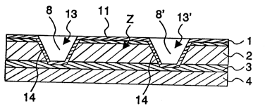
Fig. 8 shows the intermediate Z according to Fig. 7 following
the plating on of a layer of plasma etching-resistant,
electrically conductive material 11. This process stage is
optional and serves either to mechanically reinforce or
electrically connect the layers of chemically more thinly
etched conductor material 1, 3. For example, thin metal
-2137861
- 10
layers of copper or palladium can be plated on as plasma
etching-resistant, electrically conductive material 11.
The intermediate Z is suitable for the production of printed
circuit boards and film boards. With the thus reinforced con-
ductor material layers 1, 3, 11 it can undergo structuring in
current paths and interfacial connections e.g. using the
DYCOstrate~ process. Such structures can be current paths in
conductor material layers, but can also be interfacial con-
nections in openings of insulating material layers, so that
different layers of structured conductor material can be
electrically interconnected. Numerous implementation possi-
bilities are available to the expert with the knowledge of the
present invention.
The openings 8, 8' according to Fig. 8 are blind holes with
sloping walls 14, 14' relative to the flat extension of the
intermediate Z which, after plating on, electrically inter-
connect the conductor material layers 1, 3 as interfacial
connections 13, 13' and have corresponding sloping walls 14,
14' relative to the flat extension of the intermediate Z.
Such sloping walls 14, 14' can be better photochemically
structured in further production stages. Such sloping walls
14, 14' can also be more easily cleaned. In addition, such
sloping walls 14, 14' are more reliable against disturbing
external influences. On extending the insulating material
layer 2 in the Z-direction, e.g. due to a temperature rise
during soldering, sloping walls do not fracture as easily at
the corners and edges as vertical walls.
During photochemical structuring sloping walls 14, 14' are
better accessible through the prepared openings 7, 7l in the
conductor material 1 plated with electrically conductive
material 11. It is also possible to use negative operating
photoresists, which can be exposed in the interfacial connec-
tions 13, 13' and which are cheaper and less sensitive to
positive operating photoresists. The higher sensitivity has
2137861
the important advantage that lower exposure intensities are
required and faster exposure can take place.
The formation of openings 7, 7' in the conductor material
layer 1 according to Figs. 1 to 5 can simultaneously and in
completely identical manner be performed in the second con-
ductor material layer 3. For this purpose the intermediate Z
is not laminated onto the carrier substrate 4 at least in the
surface areas intended for this, so that at these points the
conductor material layer 3 can be photoresist-coated. This
photoresist layer is now structured in opening structures and
in the chemical etching process prepared openings are etched
in the conductor material layer in accordance with these
opening structures. In the plasma etching process openings or
structures are plasma-etched in the insulating material corre-
sponding to these prepared openings in the conductor material
layer. Such structures can then have straight or sloping
walls relative to the surface extension of the intermediate Z.
In the process stage according to Fig. 8 plating on is
possible to interfacial connections and then have straight or
sloping walls relative to the surface extension of the inter-
mediate Z.