Note: Descriptions are shown in the official language in which they were submitted.
2137873
- 1 - CFO 9749 ~S
Electron Source and Electron Beam Apparatus
BACKGROUND OF THE INVENTION
Field of the Invention
The present invention relates to an electron
source and an electron beam apparatus using the
electron source.
Related Background Art
Generally, an image-forming apparatus utilizing
electrons requires an enclosure for maintaining a vacuum
atmosphere therein, an electron source for emitting
electrons and a drive circuit for the electron source,
an image-forming member such as a fluorescent substance
which emits light upon impingement of electrons
thereon, and an accelerating electrode and a high-
voltage power supply for accelerating electrons toward
the image-forming member. Some of image-forming
apparatus using flat enclosures, such as thin-type
image display devices, employs support posts (spacers)
to provide a structure endurable against the
atmospheric pressure.
In such an image-forming apparatus, when electrons
are accelerated to fly in the enclosure, residual gas,
etc. residing in the vacuum atmosphere and on the
fluorescent substance are ionized and created positive
ions are accelerated by the accelerating electrode to
fly toward the electron source. If the positive ions
- - 2 - 2137873
impinge upon the electron source, particularly an
electron-emitting device having an electron-emitting
region, the electron source is deteriorated.
Therefore, to prevent charged particles from directly
impinging upon the electron-emitting device is
important in achieving longer service life and higher
reliability of the electron source.
As one expedient for preventing deterioration of
the electron source due to the phenomenon described
above, USP 4,155,028 discloses an electrostatic
deflecting system. Fig. 27 shows a schematic
construction of the disclosed system. Denoted by 3011
is an electron-emitting device comprising a hot
cathode, 3012 is a first grid, 3013 is a second grid,
and 3014 is an accelerating electrode. The first and
second grids 3012, 3013 are arranged to extend at a
certain angle defined therebetween, and are supplied
with the same potential that is sufficient to draw
electrons out of the electron-emitting device, but
insufficient to create positive ions. Solid lines 3015
in Fig. 27 represent respective paths of electrons
emitted from the electron-emitting device 3011. The
electron paths are deflected near the second grid 3013
to advance toward the accelerating electrode 3014
perpendicularly. On the other hand, positive ions
produced by the accelerating electrode 3014 have larger
mass than electrons and hence are less deflected near
_ - 3 - 2137873
the second grid 3013 to follow paths indicated by
dotted lines 3016. Accordingly, the positive ions will
not directly approach the electron-emitting device
3011. Thus, in USP 4,155,028, deterioration of the
electron-emitting device is prevented by using a
plurality of control electrodes which are arranged
obliquely with respect to the electron-emitting device.
As electron-emitting devices for use in an
electron source of an image-forming apparatus, there
are also known cold cathode devices in addition to hot
cathode devices as described above. Cold cathode
devices include electron-emitting devices of field
emission type (hereinafter abbreviated to FE),
metal/insulating layer/metal type (hereinafter
abbreviated to MIM), surface conduction type, etc.
Examples of FE electron-emitting devices are
described in, e.g., W.P. Dyke 8 W.W. Dolan, "Field
emission", Advance in Electron Physics, 8, 89 (1956)
and C.A. Spindt, "Physical Properties of Thin-film
Field Emission Cathodes with Molybdenum Cones", J.
Appl. Phys., 47, 5248 (1976).
One example of MIM electron-emitting devices is
described in, for example, C.A. Mead, "The tunnel-
emission amplifier"; J. Appl. Phys., 32, 646 (1961).
One example of surface conduction electron-
emitting devices is described in, e.g., M.I. Elinson,
Radio Eng. Electron Phys., 10, 1290 (1965).
213 78 73
- 4 -
A surface conduction electron-emitting device
utilizes a phenomenon that when a thin film having a
small area is formed on a substrate and a current is
supplied to flow parallel to the film surface,
electrons are emitted from the film. As to such a
surface conduction electron-emitting device, there have
been reported, for example, one using a thin film of
Sn02 by Elinson cited above, one using an Au thin film
[G. Dittmer: "Thin Solid Films", 9, 317 (1972)], one
using a thin film of In203/Sn02 [M. Hartwell and C.G.
Fonstad: "IEEE Trans. ED Conf.", 519 (1975)], and one
using a carbon thin film [Hisashi Araki et. al.:
"Vacuum", Vol. 26, No. 1, 22 (1983)].
As a typical configuration of those surface
conduction electron-emitting devices, Fig. 28 shows the
device configuration reported by M. Hartwell in the
above-cited paper. In Fig. 28, denoted by reference
numeral 3101 is an insulating substrate. 3102 is a
thin film for forming an electron-emitting region which
comprises, e.g., a metal oxide electroconductive thin
film formed by sputtering into an H-shaped pattern. An
electron-emitting region 3103 is formed by the
energizing process called forming (described later).
In those surface conduction electron-emitting
devices, it has heretofore been customary that, before
starting emission of electrons, the electron-emitting
region forming thin film 3102 is subjected to the
2137873
- 5 -
energizing process called forming to form the electron-
emitting region 3103. The term "forming" means a
process of applying a voltage across the electron-
emitting region forming thin film 3102 to locally
destroy, deform or denature it to thereby form the
electron-emitting region 3103 which has been
transformed into an electrically high-resistance state.
The electron-emitting region 3103 comprises a crack or
the like formed in a portion of the electron-emitting
region forming thin film 3102, and electrons are
emitted from the vicinity of the crack. The electron-
emitting region forming thin film 3102 including the
electron-emitting region which has been formed by the
forming process will be hereinafter referred to as an
electron-emitting region including thin film 3104. In
the surface conduction electron-emitting device after
the forming process, a voltage is applied to the
electron-emitting region including thin film 3104 to
supply the device with a current, whereupon electrons
are emitted from the electron-emitting region 3103.
As an example in which a number of surface
conduction electron-emitting devices are formed into an
array, there is an electron source wherein surface
conduction electron-emitting devices are arranged side
by side, both ends of the devices are interconnected by
respective wirings in parallel to form one row of an
array, and a number of rows are arranged to form the
213 78'3
- 6 -
array (see, e.g., Japanese Patent Application Laid-open
No. 64-31332 in the name of the same assignee).
Meanwhile, various image-forming apparatus are
constructed by combining an electron source which has
an array of numerous surface conduction electron-
emitting devices, with a fluorescent substance as an
image-forming member which radiates visible light upon
impingement of electrons emitted from the electron
source (see, e.g., USP 5,066,883 issued to the same
assignee). This type of image-forming apparatus is
expected to become popular and take the place of CRTs,
because it is self-luminous (i.e., emission type), is
relatively easy to manufacture with a large screen
size, and has good display quality.
In an image-forming apparatus disclosed in
Japanese Patent Application Laid-open No. 2-257551 in
the name of the same assignee, for example, desired
ones of surface conduction electron-emitting devices
formed in a large number are selected by applying
appropriate drive signals to wirings (i.e., row-
directional wirings) each interconnecting the surface
conduction electron-emitting devices in parallel which
are arranged side by side, and to control electrodes
(called grids) which are disposed in a space between an
electron source and a fluorescent substance to extend
in a direction (i.e., column-direction) perpendicular
to the row-directional wirings.
2137873
SUMMARY OF THE INVENTION
To realize an image-forming apparatus using,
particularly, cold cathode devices such as surface
conduction electron-emitting devices with a simple
construction, the inventors have studied a system
wherein the surface conduction electron-emitting
devices are properly interconnected by a plurality of
row-directional wirings and a plurality of column-
directional wirings to construct an electron source of
simple matrix array in which the surface conduction
electron-emitting devices are arranged to lie in the
row-direction and the column-direction in a matrix
pattern, and appropriate drive signals are applied to
the row-directional wirings and the column-directional
wirings so that desired ones of the surface conduction
electron-emitting devices are selected and the amounts
of electrons emitted therefrom are controlled.
(First Problem)
The above image-forming apparatus using the
electron source of simple matrix array also accompanies
a possible risk that charged particles may collide
against the electron source, particularly the electron-
emitting region of the electron-emitting device,
thereby deteriorating the electron source. There is
another possible risk that because the electron source,
particularly the electron-emitting region of the
electron-emitting device, is directly exposed as viewed
2137873
_8_
from the accelerating electrode, the electron source
may be deteriorated if an accidental discharge occurs.
(Second Problem)
As a result of studying the above image-forming
apparatus using the electron source of simple matrix
array, the inventors found that the position of light
emission on a fluorescent substance as an image-forming
member (i.e., the position where electrons impinge upon
the fluorescent substance) and the shape of light
emitting portion were deviated from the design values.
When using an image-forming member for a color image,
in particular, a reduction in luminance and a color
shift were also found in some cases along with the
deviation in the position of light emission. It was
further confirmed that the above phenomenon was caused
near a support frame or support posts (spacers)
disposed between the electron source and the image-
forming member, or in peripheral edges of the image-
forming member.
In view of the problems described above, an object
of the present invention is to provide a novel image-
forming apparatus using as electron-emitting devices,
particularly, cold cathode devices such as surface
conduction electron-emitting devices, which can easily
control selection of desired devices and the amounts of
electrons emitted from the selected devices with a
simple construction, and can ensure long service life
2137873
_ g _
and high reliability without causing any deviation in
the position of light emission.
As a result of intensive studies on the above two
problems, the inventors found that the second problem,
i.e., changes in the position and shape of light
emitting portion, was also attributable to electrons
emitted from the electron source.
More specifically, while the electrons emitted
from the electron source impinge upon the fluorescent
substance as the image-forming member, they also
impinge upon residual gas in the vacuum with a low
probability. It was found that part of scattered
particles (such as ions, secondary electrons and
neutral particles) produced upon the impingement with a
certain probability collided against a portion in the
image-forming apparatus where an insulating material is
exposed, and the exposed portion was charged with
electricity. It is then thought that such a charging
gave rise to changes in the electric field near the
exposed portion and hence a deviation of the electron
path, which resulted in changes in the position and
shape of light radiated from the fluorescent substance.
Observing the situations in which the position and
shape of light radiated from the fluorescent substance
are changed, it was further confirmed that positive
charges were primarily accumulated in the above exposed
portion. This fact is thought to be caused by
2137873
- 10 -
deposition of positive ions among the scattered
particles, or release of secondary electrons produced
when the scattered particles impinge upon the above
exposed portion.
The means for solving the problems described above
and the operation of the means will be described below.
To achieve the above object, one aspect of the
present invention resides in an electron source
comprising an electron-emitting device and a shield
member disposed above said electron-emitting device,
said electron-emitting device generating an electric
field component, when energized, that is parallel to a
substrate surface on which said electron-emitting
device is disposed, said shield member allowing
electrons emitted from said electron-emitting device to
pass therethrough, but blocks off charged particles
flying toward said electron emitting device.
Another aspect of the present invention resides in
an electron beam apparatus comprising an electron-
emitting device, a shield member disposed above said
electron-emitting device and an irradiated member to
which an electron beam emitted from said electron-
emitting device is irradiated, said electron-emitting
device generating an electric field component, when
energized, that is parallel to a substrate surface on
which said electron-emitting device is disposed, said
shield member allowing electrons emitted from said
2137873
- 11 -
electron-emitting device to pass therethrough, but
blocks off charged particles flying toward said
electron emitting device.
According to the present invention, there can be
provided an image-forming apparatus wherein the shield
member is disposed between the electron source and the
image-forming member within the image-forming apparatus
to prevent particles (mainly positive ions), which are
accelerated to fly from the side of the image-forming
member toward the electron source, from depositing on
or colliding against the electron source in the main,
so that deterioration of the electron source and
accumulation of undesired charges can be avoided. The
above arrangement is also effective to prevent charges
from accumulating on other portions than the electron
source. To this end, it is only required to determine
the shape and position of the shield member in such a
manner as to cover insulating surfaces of the other
portions such as support members (spacers) which are
used to provide a structure endurable against the
atmospheric pressure.
More specifically, the inventors have accomplished
the optimum form of the present invention in view of
that, in an electron-emitting device of the type that
an electron-emitting region is formed between a pair of
device electrodes disposed side by side on a substrate
surface, such as a surface conduction electron-emitting
21378'3
- 12 -
device, the path of emitted electrons is deviated in
the direction of an electric field developed by the
pair of device electrodes with respect to the direction
normal to the electron-emitting region because the
electric field is generated parallel to the substrate
surface, and that positive ions created in the image-
forming apparatus are accelerated to fly substantially
along an electric field which is developed by a high
voltage applied between the electron source and the
image-forming member and is vertical to these
components.
In other words, with the image-forming apparatus
of the present invention, since electrons emitted from
the electron-emitting region of the electron-emitting
device are forced to fly while deviating in the
direction of an electric field developed by the pair of
device electrodes with respect to the direction normal
to the electron-emitting region, the electrons can
travel toward the image-forming member formed of a
fluorescent substance, for example, without being
blocked off by a shield electrode as the shield member
which covers the electron-emitting region from right
above, and the electron-emitting region can be
protected by the shield electrode against positive ions
produced from the image-forming member. Also, even if
there occurs an accidental discharge, deterioration of
the electron source can be prevented. In the present
2137873
- 13 -
invention, therefore, it is not required to
additionally provide the grid, as shown in Fig. 27, for
deflecting the electrons.
Accordingly, the feature of the present invention
that does not require the additional complicated
structure is especially suitable for an image-forming
apparatus using an electron source of simple matrix
array in which, as previously proposed by the
applicant, pairs of opposite device electrodes of
surface conduction electron-emitting devices, in
particular, are properly interconnected by a plurality
of row-directional wirings and a plurality of column-
directional wirings so that the surface conduction
electron-emitting devices are arranged to lie in the
row-direction and the column-direction in a matrix
pattern.
The present invention is also applicable to any
types of cold cathode devices other than surface
conduction electron-emitting devices, in which the path
of electrons is deviated from the direction right above
or perpendicular to the electron-emitting device. One
example of such other electron-emitting devices is a
field-effect electron-emitting device having a pair of
opposite electrodes formed on the surface of a
substrate where an electron source is to be made up, as
disclosed in Japanese Patent Application Laid-open No.
63-274047 filed by the assignee.
2137873
- 14 -
The present invention is further applicable to
image-forming apparatus using electrons sources of
other than simple matrix array. One example of such
image-forming apparatus is obtained by modifying an
image-forming apparatus in which desired ones of
surface conduction electron-emitting devices are
selected by using control electrodes as disclosed in
Japanese Patent Application Laid-open No. 2-257551
filed by the assignee, such that the shield electrode
of the present invention is added on the same side as
an electron source having the surface conduction
electron-emitting devices or as a face plate having a
fluorescent substrate as viewed from the control
electrode.
According to the spirit of the present invention,
the invention is not limited to image-forming apparatus
suitable for display, but may be applied to an optical
printer, which comprises a photosensitive drum, light-
emitting diodes and so on, as a light-emitting source
in place of the light-emitting diodes. In this case,
the image-forming apparatus can be employed as not only
a linear light-emitting source, but also a two-
dimensional light-emitting source by properly selecting
a number m of row-directional wirings and a number n of
column-directional wirings.
In addition, according to the spirit of the
present invention, the invention is further applicable
2137873
- 15 -
to the case where the irradiated member to which
electrons emitted from the electron source are
irradiated is one other than the image-forming member,
such as represented by an electron microscope, for
example. Thus, the present invention can also be
practiced in the form of an electron beam generator
without specifying a type of the irradiated member.
BRIEF DESCRIPTION OF THE DRAWINGS
Figs. lA through 1C are basic schematic views
showing one example of an electron source according to
the present invention.
Figs. 2A through 2D are views of successive steps
for explaining a manufacture method of the
electronsource shown in Fig. 1.
Fig. 3 is a chart showing one example of a voltage
waveform applied in the forming process.
Fig. 4 is a schematic view showing an outline of
an apparatus for measuring and evaluating electron
emitting characteristics of an electron-emitting
device.
Fig. 5 is a graph showing current versus voltage
characteristics of the electron-emitting device.
Fig. 6 is a schematic view of an electron source
in which a number of electron-emitting devices are
arranged and connected in a simple matrix wired
pattern.
2137873
- 16 -
Fig. 7 is a perspective view, partly broken away,
showing one example of construction of an image-forming
apparatus of the present invention.
Figs. 8A and 8B are views showing examples of
configuration of a fluorescent film in the image-
forming apparatus.
Fig. 9 is a block diagram showing one example of
construction of an image display device according to
the present invention.
Fig. 10 is a partial perspective view of an
electron source shown as Example 1.
Figs. 11A and 11B are partial sectional views of
the electron source.
Figs. 12A and 12B are respectively a schematic
perspective and sectional view of the electron source
as Example 2.
Fig. 13 is a perspective view, partly broken away,
showing one example of construction of an image-forming
apparatus as Example 3.
Fig. 14 is a partial perspective view of the
image-forming apparatus shown in Fig. 13.
Fig. 15 is a sectional view of the image-forming
apparatus shown in Fig. 13.
Fig. 16 is a partial perspective view of an image-
forming apparatus as a modification of Example 3.
Fig. 17 is a sectional view of the image-forming
apparatus shown in Fig. 16.
2137873
_ 1~ _
Fig. 18 is a partial plan view of an electron
source shown as Example 4.
Fig. 19 is a partial sectional view of the
electron source shown in Fig. 18.
Figs. 20A through 20M are sectional views for
explaining successive manufacture steps of the electron
source shown in Fig. 18.
Fig. 21 is a partial showing a mask used in the
manufacture step of the electron source shown in Fig.
18.
Fig. 22 is a partial perspective view of an
electron source shown as Example 5.
Fig. 23 is a sectional view of an image-forming
apparatus constructed by using the electron source
shown in Fig. 22.
Figs. 24A and 24B are partial sectional views of
the electron source shown in Fig. 22.
Fig. 25 is a partial perspective view of a face
plate shown as Example 6.
Fig. 26 is a partial sectional view of an image-
forming apparatus shown as Example 5.
Fig. 27 is a schematic view showing construction
of a prior art electron source.
Fig. 28 is a schematic view showing construction
of a prior art electron-emitting device.
2137873
- lg -
DETAILED DESCRIPTION OF THE PREFERRED EMBODIMENTS
The present invention is directed to an electron
source, an electron beam generator and an image-forming
apparatus using the aforementioned cold cathode
devices. In particular, surface conduction electron-
emitting devices are preferably used as cold cathode
devices.
In FE devices, it is needed to control precisely
the shape of the tip of an electron emitting portion.
This necessity will increase the production cost of a
device or make it difficult to manufacture a large area
apparatus due to limitations in the production process.
On the other hand, surface conduction electron emitting
devices have a simple structure and therefore, even a
large area apparatus can be easily manufactured. Thus,
they are suitable as cold cathode devices particularly
in recent years when inexpensive, large screen display
devices are highly desired.
Further, surface conduction electron emitting
devices can be driven by application of lower voltages
(20 V or lower) than FE devices (about 100 V), which is
desirable in the present invention. Because, as the
driving voltage becomes higher, the electric field
formed by the device electrodes becomes stronger and
the deviation of electron orbitals from the vertical
direction of the device is enlarged as follows:
2137873
- 19 -
8 = 2 d Vf Vv
8: deviation;
d: height from device to opening;
Vf: device-driving voltage;
V~: potential difference between opening
and electron emitting region.
Thus, the opening position of the shield member as
in Example 1 described later will be considerably apart
from the position of the electron emitting device. In
the case that a plurality of electron emitting devices
are provided in parallel, devices must be provided with
a longer interval and it would be difficult to realize
a higher density arrangement of devices.
Further, the inventors have also found out that it
is preferable for having good characteristics and
realizing a large screen to form the electron-emitting
region or the region surrounding it of the surface
condition electron-emitting device from a fine particle
film.
Accordingly, in the following description as to
the embodiments and examples of the present invention,
image-forming apparatuses having as a multi-electron-
beam source surface conduction electron-emitting
devices formed by using a fine particle film are
described as preferred examples of the image-forming
apparatus of the present invention.
2137873
- 20 -
First, one example of construction of an electron
source according to the present invention is shown in
Figs. lA through 1C in which: Fig. lA is a plan view
and Figs. 1B and 1C are sectional views. In these
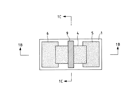
drawings, denoted by reference numeral 1 is a
substrate, 5 and 6 are device electrodes, 4 is a
conductive film including an electron-emitting region,
3 is an electron-emitting region, and 9 is a shield
member covering the electron-emitting region from right
above. Thus Figs. 1A to 1C show an example of the
electron source wherein a surface conduction electron-
emitting device, which has the conductive film 4
including the electron-emitting region 3 between the
device electrodes 5 and 6 disposed side by side on the
substrate 1, and the shield member 9 are arranged in a
unitary structure.
One example of a manufacture method of the
electron source shown in Figs. lA to 1C will be
described below with reference to Figs. 2A through 2D
(sectional view taken along line 1B-1B in Fig. lA) that
show successive manufacture steps. The following steps
a through d correspond respectively to Figs. 2A through
2D.
Step a: The substrate 1 is sufficiently washed
with a detergent, pure water and an organic solvent. A
device electrode material is then deposited on the
substrate 1 by vacuum evaporation, sputtering or any
2137873
- 21 -
other suitable method. The device electrodes 5, 6 are
then formed on the surface of the substrate 1 by the
photolithography technique.
The substrate 1 may be of, for example, a glass
substrate made of, e.g., quartz glass, glass having a
reduced content of impurities such as Na, soda lime
glass and soda lime glass having SiOz laminated thereon
by sputtering, or a ceramic substrate made of, e.g.,
alumina.
The device electrodes 5, 6 may be made of any
material which has conductivity. Examples of electrode
materials are metals such as Ni, Cr, Au, Mo, W, Pt, Ti,
A1, Cu and Pd or alloys thereof, printed conductors
comprising metals such as Pd, Ag, Au, RuOz and Pd-Ag or
oxides thereof, glass, etc., transparent conductors
such as Inz03-Sn02, and semiconductors such as
polysilicon.
Step b: Between the device electrodes 5 and 6
provided on the substrate l, an organic metal thin film
is formed by coating an organic metal solution over the
substrate. After that, the organic metal thin film is
heated for baking and then patterned by lift-off or
etching to thereby form an electron-emitting region
forming thin film 2.
The organic metal solution is a solution of an
organic compound containing, as a primary element, any
of the above-cited metals such as Pd, Ru, Ag, Au, Ti,
2137873
- 22 -
In, Cu, Cr, Fe, Zn, Sn, Ta, W and Pb.
While the organic metal thin film is formed herein
by coating the organic metal solution, the forming
method is not limited to the coating, and the organic
metal thin film may be formed by any of other methods
such as vacuum evaporation, sputtering, chemical vapor-
phase deposition, dispersion coating, dipping and
spinning.
Step c: A protective layer 7 for the electron-
emitting region forming thin film 2 is formed of Cr.
Thereafter, a sacrifice layer 8 and a shield member 9
are successively laminated thereon. At this time, the
sacrifice layer 8 and the shield member 9 are selected
in size and configuration so that the shield member 9
has opposite ends formed to reach the substrate 1. The
shield member 9 is preferably conductive and made of a
metal, e.g., A1, in the form of a thin film.
Step d: The sacrifice layer 8 is etched away to
form a gap between the thin film 2 and the shield
member 9. The protective layer 7 serving to protect
the thin film 2 during the etching is then removed.
Finally, the energizing process called forming is
carried out by applying a voltage between the device
electrode 5 and 6 from a power supply (not shown). The
electron-emitting region forming thin film 2 is thereby
locally changed in its structure so as to form the
electron-emitting region 3. Note that the electron-
2137873
- 23 -
emitting region 3 formed as described above comprises
conductive fine particles in some cases.
Practical examples of materials of the conductive
film 4 including the electron-emitting region are
metals such as Pd, Ru, Ag, Au, Ti, In, Cu, Cr, Fe, Zn,
Sn, Ta, W and Pb, oxides such as PdO, SnOz, In203, PbO,
Sb203, borides such as HfB2, ZrB2, LaBb, CeBb, YB4 and
GdB4, carbides such as TiC, ZrC, HfC, TaC, SiC and WC,
nitrides such as TiN, ZrN and HfN, semiconductors such
as Si and Ge, and carbon. The conductive film 4 is
basically of a fine particle film.
In the electron source manufactured through the
above steps, electrons are emitted from the electron-
emitting region 3 by applying a voltage to the
conductive film 4 including the electron-emitting
region so that a current flows along the device
surface. Because of a horizontal electric field
established by the device electrodes 5, 6 in the
vicinity of the electron-emitting region 3, the emitted
electrons are forced to fly following the path deviated
from the direction right above or perpendicular to the
electron-emitting region 3. Therefore, the electrons
are not blocked off by the shield member 9 which is
disposed to cover the electron-emitting region 3 from
right above. In this connection, it is desired that
the shield member 9 be associated with voltage applying
means to regulate a potential of the shield member.
2137873
- 24 -
The method of manufacturing the electron source of
the present invention is not limited to the above-
described one, but part of the foregoing manufacture
process may be modified as needed.
A method of evaluating the electron source of the
present invention will now be described with reference
to Fig. 4.
Fig. 4 is a schematic view of a
measuring/evaluating apparatus for measuring electron
emission characteristics of the electron source
constructed as shown in Figs. lA through 1C. In Fig.
4, denoted by 1 is a substrate, 5 and 6 are device
electrodes, 4 is a conductive film including an
electron-emitting region, 3 is an electron-emitting
region, and 9 is a shield member. Further, 41 is a
power supply for applying a device voltage Vf to the
electron source, 40 is an ammeter for measuring a
device current If flowing through the electron-emitting
region including conductive film 4 between the device
electrodes 5 and 6, 44 is an anode electrode for
capturing an emission current Ie emitted from the
electron-emitting region 3 of the electron source, 43
is a high-voltage power supply for applying a voltage
to the anode electrode 44, and 42 is an ammeter for
measuring the emission current Ie emitted from the
electron-emitting region 3 of the electron source. For
measuring the device current If and the emission
213~'8~~
_ - 25 -
current Ie of the electron source, the power supply 41
and the ammeter 40 are connected to the device
electrodes 5, 6, and the anode electrode 44 connected
to the power supply 43 and the ammeter 42 is disposed
above the electron source. The electron source and the
anode electrode 44 are disposed in a vacuum apparatus
which is associated with additional necessary units
(not shown) such as an evacuation pump and a vacuum
gauge, so that the electron source is measured and
evaluated under a desired degree of vacuum.
The measurement was performed by setting the
voltage applied to the anode electrode to be in the
range of 1 kV to 10 kV, and the distance H between the
anode electrode and the electron-emitting device to be
in the range of 2 mm to 8 mm.
Fig. 5 shows typical examples of the relationships
of the emission current Ie and the device current If
versus the device voltage Vf measured by the
measuring/evaluating apparatus shown in Fig. 4. Note
that the graph of Fig. 5 is plotted in arbitrary units
because values of If and Ie are much different from
each other.
Next, an electron beam generator and an image-
forming apparatus of the present invention will be
described below.
Fig. 6 is a schematic view of an electron source
in which a number of electron-emitting devices 74 are
2137873
- 26 -
arranged and connected in a simple matrix wired
pattern. In Fig. 6, denoted by 71 is a substrate
formed of a glass substrate or the like. The size and
thickness of the substrate 71 are appropriately set
depending on, for example, the number of electron-
emitting devices to be arrayed on the substrate 71, the
shape of each device in design, and conditions for
maintaining a vacuum in an enclosure when the substrate
constitutes part of the enclosure in use of the
electron source. Note that while shield members as the
main feature of the present invention are not shown in
Figs. 6 and 7 (described later) for convenience of the
drawing, each of the electron-emitting devices 74
includes the above-described shield member as shown in
Figs. lA through 1C .
Then, m lines of X-directional wirings 72,
indicated by DX1, DX2, . . . , DXm, are made of, e. g. , a
conductive metal and are formed in a desired pattern on
the substrate 71 by vacuum evaporation, printing,
sputtering or the like. The material, film thickness
and width of the wirings 72 are selected so that a
voltage as uniform as possible is supplied to all of
the numerous electron-emitting devices. Also, n lines
of Y-directional wirings 73, indicated by DY1, DY2,...,
DYn, are made of, e.g., a conductive metal and are
formed in a desired pattern on the substrate 71 by
vacuum evaporation, printing, sputtering or the like,
2137873
_. - 27 -
as with the X-directional wirings 72. The material,
film thickness and width of the wirings 73 are also
selected so that a voltage as uniform as possible is
supplied to all of the numerous electron-emitting
devices. An interlayer insulating layer (not shown) is
interposed between the m lines of X-directional wirings
72 and the n lines of Y-directional wirings 73 to
electrically isolate the wirings 72, 73 from each
other, thereby making up a matrix wired pattern. Note
that m, n are each a positive integer. The not-shown
interlayer insulating layer is made of, e.g., SiOz which
is formed by vacuum evaporation, printing, sputtering
or the like into a desired shape so as to cover the
entire or partial surface of the substrate 71 on which
the X-directional wirings 72 have been formed. The
thickness, material and fabrication process of the
interlayer insulating layer is appropriately selected
so as to endure the potential difference in portions
where the m lines of X-directional wirings 72 and the n
lines of Y-directional wirings 73 are crossed each
other.
Further, opposite electrodes (not shown in Fig. 6,
but corresponding to the above-described members 5, 6
shown in Figs. lA to 1C) of the electron-emitting
devices 74 are electrically connected to the m lines of
X-directional wirings 72 and the n lines of Y-
directional wirings 73 by respective connecting leads
__ - 28 -
75 which are made of, e.g., a conductive metal and
formed by vacuum evaporation, printing, sputtering or
the like.
The X-directional wirings 72 are electrically
connected to scan signal generating means (not shown)
for applying a scan signal to optionally scan rows of
the electron-emitting devices 74 which are arrayed in
the X-direction per row. On the other hand, the Y-
directional wirings 73 are electrically connected to
modulation signal generating means (not shown) for
applying a modulation signal to optionally modulate
columns of the electron-emitting devices 74 which are
arrayed in the Y-direction per column. Additionally, a
driving voltage applied to each of the electron-
emitting devices is supplied as a differential voltage
between the scan signal and the modulation signal both
applied to that device.
As one application of the electron beam generator
using the electron source shown in Fig. 6, an image-
forming apparatus in which an image-forming member is
employed as a member irradiated by electrons will be
described below with reference to Figs. 7, 8A and 8B.
Fig. 7 shows a basic structure of the image-forming
apparatus and Figs. 8A and 8B show patterns of a
fluorescent film used in the image-forming apparatus.
In Fig. 7, denoted by 81 is an electron source
constructed as shown in Fig. 6, 82 is a rear plate to
._ - 29 -
which the electron source 81 is fixed, 90 is a face
plate fabricated by laminating a fluorescent film 88
and a metal back 89 on an inner surface of a glass
substrate 87, and 83 is a support frame. The rear
plate 82 and the face plate 90 are joined to the
support frame 83 in a hermetically sealed manner by
using frit glass or the like to thereby make up an
enclosure 91.
In the illustrated embodiment, the enclosure 91 is
made up by the face plate 90, the support frame 83 and
the rear plate 82 as described above. However, since
the rear plate 82 is provided for the purpose of mainly
reinforcing the strength of the electron source 81, the
separate rear plate 82 can be dispensed with when the
electron source 81 itself has a sufficient degree of
strength. In this case, the support frame 83 may be
directly joined to the electron source 81 in a
hermetically sealed manner, thereby making up the
enclosure 91 by the face plate 90, the support frame 83
and the electron source 81.
The fluorescent film 88 comprises only a
fluorescent substance in the monochrome case, but in
the case of producing a color image, the fluorescent
film is formed by a combination of black conductors 92
and fluorescent substances 93, the black conductors
being called black stripes or a black matrix depending
on the manner in which the fluorescent substances are
2137873
- 30 -
arranged between the black conductors as shown in Figs.
8A and SB. The provision of the black stripes or the
black matrix is to make black the gaps between the
fluorescent substances 93 for three primary colors
which are required in color display, so that color
mixing becomes less conspicuous and a reduction in
. contrast caused by reflection of exterior light by the
fluorescent film 88 is suppressed. Materials of the
black stripes are not limited to a material containing
graphite as a primary component which is usually
employed in the art, but may be of any other material
so long as it is conductive and has small values of
transmissivity and reflectivity of light.
Fluorescent substances are coated on the glass
substrate 87 by the precipitation or printing method
regardless of whether the image is monochrome or
colored.
On the inner surface of the fluorescent film 88,
the metal back 89 is usually disposed. The metal back
89 has functions of increasing the luminance by mirror-
reflecting light, that is emitted from the fluorescent
substance to the inner side, toward the face plate 90,
serving as an electrode to apply a voltage for
accelerating an electron beam, and protecting the
fluorescent substance from being damaged by collisions
with negative ions produced in the enclosure. The
metal back can be fabricated, after forming the
2137873
- 31 -
fluorescent film, by smoothing the inner surface of the
fluorescent film (this step being usually called
filming) and then depositing A1 thereon by vacuum
evaporation, for example. To increase conductivity of
the fluorescent film 88, the face plate 90 may include
a transparent electrode (not shown) disposed on an
outer surface of the fluorescent film 88 in some cases.
Before the above hermetic sealing, alignment of
the parts with due care is required in the case of
color display since the fluorescent substances in
respective colors and the electron-emitting devices
must be precisely positioned corresponding to each
other.
The enclosure 91 is evacuated through an
evacuation tube (not shown) to create a vacuum at a
degree of about 10-6 Torr, and is then hermetically
sealed.
Additionally, to maintain a vacuum degree in the
enclosure 91 after hermetically sealing it, the
enclosure may be subjected to Bettering. This process
is performed by, immediately before or after the
sealing, heating a Better disposed in a predetermined
position (not shown) in the enclosure 91 with
resistance heating or high-frequency heating so as to
form an evaporation film of the Better. The Better
usually contains Ba as a primary component. The
interior of the enclosure 91 can be maintained at a
2137873
g2
vacuum degree in the range of 1 x 10⁻⁵ to 1 x 10-' Torr
by the adsorbing action of the evaporation film.
In the image-forming apparatus of the present
invention thus completed, voltages are applied to
desired ones of the electron-emitting devices through
terminate Doxl to Doxm and Doyl to Doyn extending
_ outwardly of the enclosure, thereby emitting electrons
therefrom. Simultaneously, a high voltage of several
kV or more is applied to the metal back 89 or the
transparent electrode (not shown) through a high-
voltage terminal Hv so that electron beams are
accelerated to impinge upon the fluorescent film 88,
whereby the fluorescent substances are excited to
radiate lights for displaying an image. Positive ions
produced near the face plate 90 at this time are forced
to fly following the path along a Z-directional
electric field established by the applied high voltage.
Thus, the positive ions flying toward each electron-
emitting region of the electron-emitting device 74 can
be blocked off by the shield member 9 provided for each
of the electron-emitting devices as shown in Figs. lA
through 1C.
Generally, the voltage applied between the pair of
device electrodes of the electron-emitting device is in
the range of 12 to 16 V, the distance between the metal
back or the transparent electrode and the electron-
emitting device is in the range of 2 to 8 mm, and the
2137873
a. - 33 -
high voltage applied between the metal back or the
transparent electrode and the electron-emitting device
is in the range of 1 to 10 kV. Preferably, the shield
member 9 is disposed nearer to the electron-emitting
device and its potential is set to be substantially
equal to the potential developed at the position of the
shield member when the shield member is not provided.
However, even if the potential of the shield member is
out of the above condition, the advantage of the
present invention is not lost so long as the emitted
electrons are not blocked off by the shield member.
Also, insofar as the shield member 9 will not block off
the emitted electrons, it may be disposed to cover not
only the area right above the electron-emitting region,
but also part or the whole of the areas right above the
electron-emitting region including conductive film 4
and the device electrodes 5, 6.
The above-described arrangement is a minimum
outline necessary to manufacture the image-forming
apparatus suitable for image display and other
purposes. Details of the apparatus, e.g., materials
and locations of the components, are not limited to
those described above, but may be selected, as desired,
to be fit for the application of the image-forming
apparatus.
[Examples]
The present invention will be described below in
213773
- 34 -
more detail in connection with Examples.
Example 1
Fig. 10 shows a schematic partial perspective view
of an electron source of this Example. Sectional views
taken respectively along lines 11A-11A and 11B-11B in
Fig. 10 are shown in Figs. 11A and 11B. Note that, in
Figs. 6, 10, 11A and 11B, the same reference numerals
denote identical members. Referring to the drawings,
denoted by 71 is an insulating substrate, 73 is a Y-
directional wiring formed in a predetermined pattern on
the insulating substrate 71, 72 is an X-directional
wiring which had a film thickness of 50 dam and was
formed by, e.g., printing on the Y-directional wiring
73 with an interlayer insulating layer (not shown)
therebetween, and 74 is an electron-emitting device.
The electron-emitting device 74 was of a surface
conduction electron-emitting device which had the
conductive film 4 including the electron-emitting
region 3 between the device electrodes 5 and 6 disposed
side by side, as described above with reference to
Figs. lA through 1C. A number of electron-emitting
devices 74 were electrically connected, as shown in
Fig. 10, to the X-directional wirings 72 and the Y-
directional wirings 73 by connecting leads 75.
Further, denoted by 9 is a shield member which was
formed of a conductive thin plate (of, e.g., A1) and
was disposed on the X-directional wirings 72 with an
213773
- 35 -
insulating layer (not shown) therebetween. The shield
member 9 had electron passage holes 10 formed therein
so as to cover the areas right above the electron-
emitting devices 74, but not to interfere with the
paths of electrons emitted from the electron-emitting
regions of the electron-emitting devices.
Specifically, the electron passage holes 10 formed in
the shield member 9 were each circular with a radius of
30 um and had the center at a position deviated 40 um
(indicated by S2 in Fig. 11B) from the position right
above the corresponding electron-emitting region.
The manufacture process of the electron source of
this Example will be briefly described in the order of
successive steps.
1) A silicon oxide film being 0.5 um thick was formed
on a cleaned soda lime glass, as the substrate 71, by
sputtering. A Cr film being 50 ~ thick and an Au film
being 6000 ~ thick were then laminated on the substrate
71 in this order by vacuum evaporation. A photoresist
(AZ1370, by Hoechst Co.) was coated thereon under
rotation by using a spinner and then baked.
Thereafter, by exposing and developing a photomask
image, a resist pattern for the Y-directional wirings
73 was formed. The deposited Au/Cr films were
selectively removed by wet etching to thereby form the
Y-directional wirings 73 in a desired pattern.
2) Then, the interlayer insulating layer (not shown)
- 3g _ 2137873
formed of a silicon oxide film being 1.0 um thick was
deposited over the substrate by RF sputtering.
3) A photoresist pattern for forming contact holes
(not shown) in the above silicon oxide film for
electrical connection between the Y-directional wirings
73 and the device electrodes was coated thereon and, by
using it as a mask, the interlayer insulating layer was
selectively etched to form the contact holes. The
etching was carried out by the RIE (Reactive Ion
Etching) process using a gas mixture of CF4 and HZ.
4) A photoresist (RD-2000N-41, by Hitachi Chemical
Co., Ltd.) was formed in a pattern to define the device
electrodes 5, 6 and the gaps therebetween. A Ti film
being 50 ~ thick and an Ni film being 1000 ~ thick were
then deposited thereon in this order by vacuum
evaporation. The photoresist pattern was dissolved in
an organic solvent to leave the deposited Ni/Ti films
by lift-off, whereby the device electrodes 5, 6 were
formed.
5) The X-directional wirings 72 of silver were formed
in a desired pattern with a thickness of 50 dam by
screen printing.
6) By using a mask formed with openings each covering
the gap between the device electrodes and the vicinity
thereof, a Cr film being 1000 ~ thick was deposited by
vacuum evaporation and patterned. Organic Pd (ccp-
4230, by Okuno Pharmaceutical Co., Ltd.) was coated
- 37 - 2137873
thereon under rotation by using a spinner and then
heated for baking at 300~C for 10 minutes. An
electron-emitting region forming thin film comprising
fine particles of Pd as a primary constituent element
was thus formed.
7) The Cr film and the electron-emitting region
forming thin film after the baking were etched by an
acid etchant to provide the electron-emitting region
forming thin film in a desired pattern.
8) A resist was coated over the entire surface,
exposed by using a mask, and then developed to form a
resist pattern in which the resist was removed in only
the areas corresponding to the contact holes. A Ti
film being 50 ~ thick and an Au film being 5000 ~1 thick
were then deposited thereon in this order by vacuum
evaporation. The unnecessary deposits on the resist
pattern was removed to leave the contact holes filled
with the deposits by lift-off.
As a result of the above steps, the Y-directional
wirings 73, the interlayer insulating layer (not
shown), the X-directional wirings 72, the device
electrodes 5, 6, the electron-emitting region forming
thin films, etc. were formed on the insulating
substrate 71 to provide the electron source not yet
subjected to the forming process.
Subsequently, the shield member 9 formed of a
conductive thin plate (of, e.g., A1) was disposed on
__ - 38 _ 2~~~~'~
the X-directional wirings 72 at a predetermined
position with an insulating layer (not shown)
therebetween.
A description will now be made, with reference to
Figs. 7, 8A and 8B, of an example in which a display
device is made up by using the electron source
manufactured as above and not yet subjected to the
forming process.
First, the electron source 81 not yet subjected to
the forming process was fixed onto a rear plate 82.
Then, a face plate 90 (comprising a fluorescent film 88
as an image-forming member and a metal back 89
laminated on an inner surface of a glass substrate 87)
was disposed 5 mm above the electron source 81 through
a support frame 83. After applying frit glass to
joined portions between the face plate 90, the support
frame 83 and the rear plate 82, the assembly was baked
in the atmosphere at temperature of 400°C to 500°C for
10 or more minutes for hermetically sealing the joined
portions (see Fig. 7). Frit glass was also used to fix
the electron source 81 to the rear plate 82.
While the fluorescent film 88 as the image-forming
member comprises only a fluorescent substance in the
monochrome case, it was fabricated in this Example by
employing a stripe pattern of fluorescent substances
and black conductors (see Figs. 8A and 8B). The
stripes of black conductors were formed by using a
213?873
_. _ 3g
material containing graphite as a primary component
which is usually employed in the art. Fluorescent
substances were coated on the glass substrate 87 by the
slurry method.
After forming the fluorescent film 88, the metal
back 89 was formed on the inner surface of the
fluorescent film by smoothing the inner surface of the
fluorescent film (this step being usually called
filming) and then depositing Al thereon by vacuum
evaporation. To increase conductivity of the
fluorescent film 88, the face plate 90 may include a
transparent electrode (not shown) on an outer surface
of the fluorescent film 88 in some cases. However,
such a transparent electrode was not provided in this
Example because sufficient conductivity was obtained
with the metal back only. Before the above hermetic
sealing, alignment of the respective parts was carried
out with due care since the fluorescent substances in
respective colors and the electron-emitting devices
must be precisely positioned relative to each other in
the case of color display.
The atmosphere in the glass enclosure thus
completed was evacuated by a vacuum pump through an
evacuation tube (not shown). After reaching a
sufficient degree of vacuum, a voltage was applied
between the electrodes 5 and 6 of the electron-emitting
devices 84 through terminals Doxl to Doxm and Doyl to
2137873
- 40 -
Doyn extending outwardly of the enclosure for producing
the electron-emitting regions 3 through the
energization process (forming process) of the electron-
emitting region forming thin films 2. The voltage
waveform used for the forming process was shown in Fig.
3.
Referring to Fig. 3, T1 and TZ represent a pulse
width and a pulse interval of the voltage waveform,
respectively. In this Example, T1 and TZ were set
respectively to 1 millisecond and IO milliseconds, and
a crest value of the triangular waveform (i.e., a peak
voltage during the forming process) was set to 5 V.
Then, the forming process was carried out for 60
seconds in a vacuum atmosphere of about 1 x 10'6 Torr.
Next, at a vacuum degree of about 10'6 Torr, the
evacuation tube (not shown) was heated and fused
together by using a gas burner to hermetically seal the
enclosure.
Finally, to maintain a desired vacuum degree in
the enclosure after sealing off it, the enclosure was
subjected to Bettering.
In the image display device thus completed, a scan
signal and a modulation signal were applied from
respective signal generating means (not shown) to
desired ones of the electron-emitting devices through
the terminals Doxl to Doxm and Doyl to Doyn extending
outwardly of the enclosure, thereby emitting electrons
2137873
- 41 -
therefrom. Simultaneously, a high voltage was applied
to the metal back 89 through a high-voltage terminal Hv
so that electron beams were accelerated to impinge upon
the fluorescent film 88. The fluorescent substances
making up the film 88 were thereby excited to radiate
lights for displaying an image. The voltage applied to
the high-voltage terminal Hv was set to 5 kV, the
voltage applied to the shield member 9 was set to 50 V,
and the voltage applied between the pairs of device
electrodes 5 and 6 was set to 14 V.
Under the above condition, because of a horizontal
electric field established by the device electrodes 5,
6 in the vicinity of the electron-emitting region,
electrons emitted from each of the electron-emitting
regions 3 were forced to fly following the path
deviated from the direction right above or
perpendicular to the electron-emitting region 3 and
hence were not blocked off by the shield member 9. On
the other hand, positive ions produced near the face
plate 90 were forced to fly following the path along a
vertical electric field established by the applied high
voltage, and hence could be blocked off by the shield
member 9. Thus, there occurred no damage of the
electron-emitting region 3 due to the positive ions.
In this Example, since the shield member 9 covered
the areas right above parts of the device electrodes 5,
6 (see Figs. lA through 1C), the connecting leads 75
213783
- 42 -
and the wirings 72, 73, in addition to the areas right
above the electron-emitting regions 3 (see Figs. lA
through 1C), no damages of the former members were
found. It covered also parts of the exposed insulating
surface 71 and therefore, no electric charge was
generated at this position. It was also confirmed that
by changing the electron passage holes 10 in shape and
position, the electron beams could be shaped and/or
deflected as desired.
Example 2
Figs. 12A and 12B show an image-forming apparatus
of this Example 2 in which: Fig. 12A is a perspective
view showing a portion of the apparatus, and Fig. 12B
is a sectional view taken along line 12B-12B in Fig.
12A. The image-forming apparatus of this Example 2 was
different from that of Example 1 in that, as shown in
Fig. 12A, four substrates 81a to 81d each constituting
an electron source were combined with each other to
make up an entire electron source. Note that other
components than the electron source, such as the rear
plate 82, the support frame 83 and the face plate 90,
were identical to those in Example 1.
The 12B-12B section shown in Fig. 12A is viewed in
the same direction as the 11A-11A section in Fig. 10.
Each of the electron sources 81a - 81d had basically
the same structure as the electron source shown in
Figs. 10, 11A and 11B. As shown in Fig. 12B, for
.. ~ 2137873
- 43 -
example, an electrode plate 9d as a shield member
disposed on X-directional wirings 72d, which were in
turn formed on a substrate 71d, with an insulating
layer (not shown) therebetween had electron passage
holes lOd for allowing electrons emitted from an
electron-emitting device 74d to pass therethrough.
As with Example 1, the shield members 9a - 9d had
electron passage holes l0a - lOd formed therein so as
to cover the respective areas right above electron-
emitting devices 74a - 74d, particularly electron-
emitting regions, but not to interfere with the
respective paths of electrons emitted from the
electron-emitting regions of the electron-emitting
devices. Specifically, the electron passage holes
l0a - lOd formed respectively in the shield members
9a - 9d were each circular with a radius of 30 um and
had the center at a position deviated 40 um from the
position right above the corresponding electron-
emitting region.
In the image display device of this Example
constructed as above, as with Example 1, a scan signal
and a modulation signal were applied from respective
signal generating means (not shown) to desired ones of
the electron-emitting devices through the terminals
Doxl to Doxm and Doyl to Doyn extending outwardly of
the enclosure, thereby emitting electrons therefrom.
Simultaneously, a high voltage was applied to the metal
0
2137873
- 44 -
back 89 through the high-voltage terminal Hv so that
electron beams were accelerated to impinge upon the
fluorescent film 88. The fluorescent substances making
up the film 88 were thereby excited to radiate lights
for displaying an image. The voltage applied to the
high-voltage terminal Hv was set to 5 kV, the voltage
applied to the shield members 9a - 9d was set to 100 V,
and the voltage applied between the pairs of device
electrodes 5 and 6 was set to 14 V.
The similar advantages as in Example 1 were also
obtained in this Example 2. Additionally, with this
Example, an image-forming apparatus capable of
displaying images on a large-sized screen could be
realized by using a plurality of electron sources and a
plurality of shield electrode members.
This Example may be modified so as to have a
plurality of shield electrode members on a single
electron source. This modification could also provide
the similar advantages as in Example 2.
Example 3
This Example concerns with an image-forming
apparatus of the type that desired ones of surface
conduction electron-emitting devices are selected by
using control electrodes which have a modulation
function as disclosed in Japanese Patent Application
Laid-open No. 2-257551 filed by the assignee, wherein
the shield electrode member of the present invention is
2137873
- 45 -
added on the same side as the electron source having
surface conduction electron-emitting devices as viewed
from the control electrode.
A schematic perspective view of the image-forming
apparatus of this Example is shown in Fig. 13. Also,
Fig. 14 shows a partial enlarged perspective view of
Fig. 13 and Fig. 15 shows a section taken along line
15-15 in Fig. 13.
Referring to the drawings, denoted by 201 is an
insulating substrate, 202 and 203 are respectively
positive and negative electrode wirings formed on the
insulating substrate 201 by, e.g., printing, and 204 is
an electron emitting device. The electron-emitting
device 204 was of a surface conduction electron-
emitting device which had the conductive film 4
including the electron-emitting region 3 between the
device electrodes 5 and 6 disposed side by side, as
described above with reference to Figs. lA through 1C.
A number of electron-emitting devices 204 were
electrically connected to the positive electrode
wirings 202 with a thickness of 50 um and the negative
electrode wirings 203 with a thickness of 50 um by
connecting leads 205.
Further, denoted by 209 is a shield member which
was formed of a conductive thin plate (of, e.g., A1)
and was disposed on the positive electrode wirings 202
and the negative electrode wirings 203 with an
2137873
- 46 -
insulating layer (not shown) therebetween. The shield
member 209 had electron passage holes 210 formed
therein so as to cover the areas right above the
electron-emitting devices 204, but not to interfere
with the paths of electrons emitted from the electron-
emitting devices 204. Specifically, the electron
passage holes 210 formed in the shield member 209 were
each circular with a radius of 30 um and had the center
at a position deviated 40 um from the position right
above the corresponding electron-emitting region.
The insulating substrate 201 and the components
formed on the substrate 201 will be referred to
together as an electron source 211.
Denoted by 207 is a stripe-shaped control
electrode disposed midway between the electron source
211 and a face plate 220 (described later) in
orthogonal relation to the positive electrode wirings
202 and the negative electrode wirings 203, and 208 is
an electron passage hole defined in each of the control
electrodes 207 corresponding to the electron-emitting
devices 204 in one-to-one relation. The control
electrodes 207 were formed on a support plate 215 and
were held by support posts 214 midway between the
electron source 211 and the face plate 220.
Denoted by 212 is a rear plate to which the
electron source 211 was fixed, 220 is a face plate
comprising a fluorescent film 218 and a metal back 219
2137873
- 47 -
laminated on an inner surface of a glass substrate 217,
and 213 is a support frame. The fluorescent film 218
used herein as an image-forming member was similar to
the fluorescent film 88 in Example 1.
In the image-forming apparatus of this Example,
the rear plate 212, the support frame 213 and the face
plate 220 were joined to each other in a hermetically
sealed manner by using frit glass to thereby constitute
an enclosure 221.
More specifically, the electron source 211 not yet
subjected to the forming process was first fixed onto
the rear plate 212. Then, the support plate 215 was
fixedly disposed above the electron source 211 through
the support posts 214. Further, the face plate 220 was
disposed at 5 mm above the electron source 211 through
the support frame 213. After applying frit glass to
joined portions between the face plate 220, the support
frame 213 and the rear plate 212, the assembly was
baked in the atmosphere or a nitrogen atmosphere at
temperature of 400~C to 500~C for 10 or more minutes
for hermetically sealing the joined portions. Frit
glass was also used to fix the electron source 211 to
the rear plate 212 and fix the support plate 215 to the
electron source 211.
Connected to respective voltage applying means
(not shown) were the positive electrode wirings 202
through terminals Dal to Dam, the negative electrode
237873
- 48 -
wirings 203 through terminals Dbl to Dbn, the control
electrodes 207 through terminals G1 to Gn, the shield
electrode 209 through a terminal Sv, and the metal back
219 through a high-voltage terminal Hv, all of these
terminals extending outwardly of the enclosure.
Before the above hermetic sealing, alignment of
the respective parts was carried out with due care
since the fluorescent substances in respective colors
and the electron-emitting devices must be precisely
positioned relative to each other in the case of color
display. The control electrodes and the electron-
emitting devices were also precisely positioned
relative to each other with due care.
The atmosphere in the glass enclosure thus
completed was evacuated by a vacuum pump through an
evacuation tube (not shown). After reaching a
sufficient degree of vacuum, a voltage was applied
between the device electrodes through the terminals Dal
to Dam and Dbl to Dbn extending outwardly of the
enclosure for producing the electron-emitting regions
through the energization process (forming process) of
the electron-emitting devices 204, as with Example 1.
Next, at a vacuum degree of about 10-6 Torr, the
evacuation tube (not shown) was heated and fused
together by using a gas burner to hermetically seal the
enclosure. To maintain a desired vacuum degree in the
enclosure after sealing off it, the enclosure was
2137873
- 49 -
subjected to Bettering.
In the image display device thus completed, scan
signals having required voltage waveforms were applied
from respective signal generating means (not shown) to
desired ones of the electron-emitting devices 204
through the terminals Dal to Dam and Dbl to Dbn
extending outwardly of the enclosure, thereby emitting
electrons therefrom, and a modulation signal having a
required voltage waveform was applied from signal
generating means (not shown) to desired one or more of
the control electrodes 207 through the terminals Gl to
Gn extending outwardly of the enclosure, thereby
controlling the amounts of electrons passed through the
electron passage holes 208. Simultaneously, a high
voltage was applied to the metal back 219 through the
high-voltage terminal Hv so that electron beams after
passing through the electron passage holes 208 were
accelerated to impinge upon the fluorescent film 218.
The fluorescent substances making up the film 218 were
thereby excited to radiate lights for displaying an
image.
The distance between the electron-emitting devices
204 of the electron source 211 and the metal back 219
was set to 5 mm, the voltage applied to the high-
voltage terminal Hv was set to 5 kV, the voltage
applied to the shield member or electrode 209 was set
to 100 V, and the voltage applied between the pairs of
217873
- 50 -
device electrodes of the electron-emitting devices 204
was set to 14V.
The similar advantages as in Example 1 were also
obtained in the Example 3. Additionally, with this
Example, potential distribution between the shield
electrode 209 and the electron-emitting devices 204
could be kept substantially uniform with the provision
of the shield electrode 209 regardless of the
modulation voltage applied to the control electrodes
207. Therefore, the image display device being more
stable in the position and shape of light flux radiated
could be realized.
One modification of this Example was obtained, as
shown in a partial enlarged perspective view of Fig. 16
and a sectional view of Fig. 17, by arranging the
shield member 209 between the face plate 220 and the
control electrodes 207. With this modification,
potential distribution between the shield electrode 209
and the face plate 220 could be kept substantially
uniform with the provision of the shield electrode 209
regardless of the modulation voltage applied to the
control electrodes 207. As a result, in addition to
the similar advantages as in Example 1, positive ions
produced near the face plate 220 could be surely
blocked off.
Example 4
The following description will be made of Example
2137873
- 51 -
4 in which an image-forming apparatus of the type shown
in Fig. 7 was manufactured by using an electron source
of the type shown in Fig. 6 that comprises a number of
electron-emitting devices including shield members as
shown in Figs. lA through 1C. Fig. 18 is a plan view
of part of the electron source and Fig. 19 is a
sectional view taken along line 19-19 in Fig. 18. Note
that, in Figs. 7, 18 and 19, the same reference
numerals denote identical members. Referring to the
drawings, denoted by 71 is an insulating substrate, 72
is an X-directional wiring, 73 is a Y-directional
wiring, 4 is a conductive film including an electron-
emitting region, 5 and 6 are device electrodes, 141 is
an interlayer insulating layer, and 142 is a contact
hole for electrical connection between the device
electrode 5 and the X-directional wiring 72.
The manufacture process of the electron source
will first be described in detail in the order of
successive steps with reference to Figs. 20A through
20M. Note that the following steps a to m correspond
to Figs. 20A through 20M, respectively.
Step a: A silicon oxide film being 0.5 um thick
was formed on a cleaned soda lime glass, as the
substrate 71, by sputtering. A Cr film being 50
thick and an Au film being 6000 ~1 thick were then
laminated on the substrate 71 in this order by vacuum
evaporation. A photoresist (AZ1370, by Hoechst Co.)
2137873
- 52 -
was coated thereon under rotation by using a spinner
and then baked. Thereafter, by exposing and developing
a photomask image, a resist pattern for the X-
directional wirings 72 was formed. The deposited Au/Cr
films were selectively removed by wet etching to
thereby form the X-directional wirings 72 in a desired
pattern.
Step b: Then, the interlayer insulating layer 141
formed of a silicon oxide film being 1.0 um thick was
deposited over the substrate by RF sputtering.
Step c: A photoresist pattern for forming the
contact holes 142 in the silicon oxide film deposited
in the above step b was coated thereon and, by using it
as a mask, the interlayer insulating layer 141 was
selectively etched to form the contact holes 142. The
etching was carried out by the RIE (Reactive Ion
Etching) process using a gas mixture of CF4 and Hz.
Step d: A photoresist (RD-2000N-41, by Hitachi
Chemical Co., Ltd.) was formed in a pattern to define
the device electrodes and the gaps therebetween. A Ti
film being 50 ~ thick and an Ni film being 1000 ~ thick
were then deposited thereon in this order by vacuum
evaporation. The photoresist pattern was dissolved in
an organic solvent to leave the deposited Ni/Ti films
by lift-off, whereby the device electrodes 5, 6 having
the electrode gap of 3 um and the electrode width of
300 um were formed.
2137873
- 53 -
Step e: A photoresist pattern for the Y-
directional wirings 73 was formed on the device
electrodes 5 and 6. A Ti film being 50 ~ thick and an
Au film being 5000 ~ thick were then deposited thereon
in this order by vacuum evaporation. The unnecessary
deposits on the photoresist pattern were removed to
form the Y-directional wirings 73 in a desired pattern
by lift-off.
Step f: Fig. 21 is a plan view of part of a mask
used in this step to form an electron-emitting region
forming thin film 2 of the electron-emitting device.
The mask has an opening covering each gap L1 between
the device electrodes and the vicinity thereof. A Cr
film 151 being 1000 ~1 thick was deposited by vacuum
evaporation and patterned by using the mask. Organic
Pd (ccp-4230, by Okuno Pharmaceutical Co., Ltd.) was
coated thereon under rotation by using a spinner and
then heated for baking at 300~C for 10 minutes.
The electron-emitting region forming thin film 2
thus formed and comprising fine particles of Pd as a
primary constituent element had a thickness of about
100 ~ and a sheet resistance value of 5 x 10⁴ S2/0. The
term "fine particle film" used herein means a film
comprising a number of fine particles aggregated
together, and includes films having microstructures in
which fine particles are not only individually
dispersed, but also adjacent to or overlapped with each
2137873
- 54 -
means a diameter of fine particles whose shape is
discernible under the above particle condition.
Step g: The Cr film 151 after the baking was
etched by an acid etchant to provide the electron-
s emitting region forming thin film 2 in a desired
pattern.
Step h: A resist was coated in a pattern to cover
the surface other than the contact holes 142. A Ti
film being 50 ~ thick and an Au film being 5000 ~ thick
were then deposited thereon in this order by vacuum
evaporation. The unnecessary deposits on the resist
pattern was removed to leave the contact holes 142
filled with the deposits by lift-off.
Step i: A protective layer 131 formed of a Cr
thin film was formed to cover the electron-emitting
region forming thin film 2.
Step j: A positive photoresist (AZ1350J, by
Hoechst Co.) was coated with a thickness of 5 um by
using a spin coater and then patterned to form a
sacrifice layer 132 which is removed in a later
described step i to provide a vacant space.
Step k: An A1 thin film serving as the shield
member 9 was formed and then patterned to have a width
(S1) of 0.5 um. The patterning was made to connect the
shield member 9 to either the device electrode 5 or 6.
Step 1: The photoresist forming the sacrifice
layer 132 was etched by the RIE process using a gas
2137873
._ - 55 -
layer 132 was etched by the RIE process using a gas
mixture of oxygen and CF4.
Step m: The Cr thin film forming the protective
layer 131 was removed by wet etching.
As a result of the above steps, the X-directional
wirings 72, the interlayer insulating layer 141, the Y-
directional wirings 73, the device electrodes 5, 6, the
electron-emitting region forming thin films 2, the
shield members 9, etc. were formed on the insulating
substrate 71.
The electron source thus manufactured and not yet
subjected to the forming process was installed in the
enclosure 91 shown in Fig. 7 and then subjected to the
forming process, followed by hermetically sealing the
enclosure and Bettering the interior of the enclosure
to construct an image display device of the type shown
in Fig. 7, as with Example 1.
In the image display device constructed as above,
as with Example 1, a scan signal and a modulation
signal were applied from respective signal generating
means (not shown) to desired ones of the electron-
emitting devices through the terminals Doxl to Doxm and
Doyl to Doyn extending outwardly of the enclosure,
thereby emitting electrons therefrom. Simultaneously,
a high voltage was applied to the metal back 89 through
the high-voltage terminal Hv so that emitted electron
beams were accelerated to impinge upon the fluorescent
2137873
- 56 -
film 88. The fluorescent substances making up the film
88 were thereby excited to radiate lights for
displaying an image. The voltage applied to the high-
voltage terminal Hv was set to 5 kV, and the voltage
applied between the pairs of device electrodes 5 and 6
was set to 14 V. Further, one of the device electrodes
5 and 6 connected to the shield member 9 was set to
have a higher potential. The similar advantages as in
Example 1 were also obtained in this Example 4.
One modification of this Example was obtained by
additionally providing a wiring connected to each
shield member 9 and means for applying a voltage to the
wiring so as to regulate a potential of the shield
member 9. With this modification, the similar
advantages as in Example 1 were resulted by applying 10
V to the shield member.
Another modification of this Example was obtained
by forming the shield member 9 to cover the whole of
the electron-emitting region including conductive film
4 or the whole of the device electrodes 5, 6. This
modification could also provide the similar advantages
as in Example 1.
Still another modification of this Example was
obtained by forming the plurality of electron-emitting
devices on the substrate, and forming the interlayer
insulating layer between the X-directional wirings and
the Y-directional wirings to only cover each of the
213'873
- 57 -
areas where the X- and Y-directional wirings
intersect, so that the device electrodes were
electrically connected to the X- and Y-directional
wirings, which were formed directly on the insulating
substrate, without using contact holes.
Example 5
The following description will be made of Example
5 in which an image-forming apparatus of the type shown
in Fig. 7 was manufactured by using an electron source
shown in Figs. 22 and 23. Fig. 22 is a schematic
perspective view of part of the electron source and
Fig. 23 is a vertical sectional view. Also, sections
taken respectively along line 24A-24A and 24B-24B in
Fig. 22 are shown in Figs. 24A and 24B, respectively.
Note that, in Figs. 7, 22, 23, 24A and 24B, the same
reference numerals denote identical members. Referring
to the drawings, denoted by 171 is a spacer provided to
keep a spacing between a substrate 71 including the
electron source and a face plate 90 including a
fluorescent film, and 9 is a rod-shaped shield member
fixed to the spacers 171. The spacers 171 were each
disposed on an X-directional wiring 72. The shield
member 9 was selected in position and size so as to
cover the areas right above electron-emitting devices
74, but not to interfere with the paths of electrons
emitted from respective electron-emitting regions of
the electron-emitting devices 74. Specifically, the
2137873
- 58 -
shield member 9 being 80 um wide (indicated by S3 in
Fig. 24A) and 80 um high (indicated by S4 in Fig. 24A)
was formed in the position spaced 200 um right above
the electron-emitting device. The distance between the
surface of the substrate 71 in which the electron-
emitting devices were formed and the metal back surface
of the face plate 90 was set to 5 mm.
It is preferable that the spacers 171 and the
shield members 9 be at least slightly conductive for
the purpose of stabilizing the potential near the
electron paths. In this Example, therefore, these
components were each prepared by spray-coating a
conductive film on the surface of a soda glass. Also,
voltage applying means (not shown) was connected to the
spacers 171 and the shield members 9 for applying a
certain voltage to them.
The shield members 9 may be integrally molded with
the spacers 171 beforehand, or joined to the spacers
during the assembly step.
In the image display device completed in a like
manner to Example 1 by using the electron source of
this Example, as with Example 1, a scan signal and a
modulation signal were applied from respective signal
generating means (not shown) to desired ones of the
electron-emitting devices through the terminals Doxl to
Doxm and Doyl to Doyn extending outwardly of the
enclosure, thereby emitting electrons therefrom.
2137873
- 59 -
Simultaneously, a high voltage was applied to the metal
back 89 through the high-voltage terminal Hv so that
emitted electron beams were accelerated to impinge upon
the fluorescent film 88. The fluorescent substances
making up the film 88 were thereby excited to radiate
lights for displaying an image. The voltage applied to
the high-voltage terminal Hv was set to 5 kV, and the
voltage applied between the pairs of device electrodes
5 and 6 was set to 14 V. The similar advantages as in
Example 1 were also obtained in this Example 5.
Additionally, there occurred no accumulation of
undesired charges on the spacers 171.
One modification of this Example was obtained by
additionally providing a wiring connected to each
shield member 9 and means for applying a voltage to the
wiring so as to regulate a potential of the shield
member 9. With this modification, the similar
advantages as in Example 1 were resulted by applying
200 V to the shield member.
Example 6
The following description will be made of Example
6 in which an image-forming apparatus of the type shown
in Fig. 7 was manufactured in a like manner to Example
1 except that a shield member provided on a face plate
90 through spacers 191, as shown in Fig. 25, was used
as the shield member 9 in the electron source (see Fig.
10) of Example 1. Fig. 25 is a schematic perspective
2137873
- 60 -
view of part of the face plate 90 provided with the
shield member 9, and Fig. 26 shows a section taken
along line 26-26 in Fig. 25, including a section of an
electron source substrate 71 located in opposite
relation to face the face plate 90. Note that, in
Figs. 7, 25 and 26, the same reference numerals denote
identical members.
The shield member 9 was made of a conductive
material (such as A1) in the mesh-like form and was
held by the spacers 191 with a certain spacing kept
relative to the face plate 90. The shield member 9 was
selected in mesh position and mesh size so as to cover
at least the areas right above electron-emitting
devices 74, but not to totally interfere with the paths
of electrons emitted from respective electron-emitting
regions of the electron-emitting devices 74. The
shield member 9 was located at the position spaced from
the face plate 90 by a distance corresponding to 10
of the spacing between the electron source substrate 71
and the face plate 90. Also, a voltage was applied
from a DC power supply (not shown) to the shield member
9 so that the potential of the shield member 9 was
equal or about 10 % lower than the potential applied to
the face plate 90.
In the image display device completed in a like
manner to Example 1 except for the above construction,
as with Example 1, a scan signal and a modulation
213~8~3
- 61 -
signal were applied from respective signal generating
means (not shown) to desired ones of the electron-
emitting devices through the terminals Doxl to Doxm and
Doyl to Doyn extending outwardly of the enclosure,
thereby emitting electrons therefrom. Simultaneously,
a high voltage over several kV was applied to the metal
back 89 through the high-voltage terminal Hv so that
emitted electron beams were accelerated to impinge upon
the fluorescent film 88. The fluorescent substances
making up the film 88 were thereby excited to radiate
lights for displaying an image. The similar advantages
as in Example 1 were also obtained in this Example 6.
Example 7
Fig. 9 is a block diagram showing one example of
an image display device in which any of the display
devices (display panels) manufactured in Examples 1 to
6 was designed to be able to display image information
provided from various image information sources
including TV broadcasting, for example. In Fig. 9,
denoted by 100 is a display panel, 101 is a driver for
the display panel, 102 is a display panel controller,
103 is a multiplexer, 104 is a decoder, 105 is an
input/output interface, 106 is a CPU, 107 is an image
generator, 108, 109 and 110 are image memory
interfaces, 111 is an image input interface, 112 and
113 are TV signal receivers, and 114 is an input unit.
(When the present display device receives a signal,
2137873
- 62 -
e.g., a TV signal, including both video information and
voice information, the device of course displays an
image and reproduces voices simultaneously. But
circuits, a speaker and so on necessary for reception,
separation, reproduction, processing, storage, etc. of
voice information, which are not directly related to
the features of the present invention, will not
described here.)
Functions of the above parts will be described
below along the flow of image signals.
First, the TV signal receiver 113 is a circuit for
receiving a TV image signal transmitted through a
wireless transmission system in the form of electric
waves or spatial optical communication, for example. A
type of the TV signal to be received is not limited to
particular one, but may be any type of the NTSC-, PAL-
and SECAM-standards, for example. Another type TV
signal (e. g., so-called high-quality TV signal
including the MUSE-standard type) having the larger
number of scan lines than the above types is a signal
source fit to utilize the advantage of the above
display panel which is suitable for an increase in the
screen size and the number of pixels. The TV signal
received by the TV signal receiver 113 is output to the
decoder 104.
Then, the TV signal receiver 112 is a circuit for
receiving a TV image signal transmitted through a wire
2137873
- 63 -
transmission system in the form of coaxial cable or
optical fibers. As with the TV signal receiver 113, a
type of the TV signal to be received by the TV signal
receiver 112 is not limited to particular one. The TV
signal received by the receiver 112 is also output to
the decoder 104.
The image input interface 111 is a circuit for
taking in an image signal supplied from an image input
device such as a TV camera or an image reading scanner,
for example. The image signal taken in by the
interface 111 is output to the decoder 104.
The image memory interface 110 is a circuit for
taking in an image signal stored in a video tape
recorder (hereinafter abbreviated to a VTR). The image
signal taken in by the interface 110 is output to the
decoder 104.
The image memory interface 109 is a circuit for
taking in an image signal stored in a video disk. The
image signal taken in by the interface 109 is output to
the decoder 104.
The image memory interface 108 is a circuit for
taking in an image signal from a device storing still
picture data, such as a so-called still picture disk.
The image signal taken in by the interface 108 is
output to the decoder 104.
The input/output interface 105 is a circuit for
connecting the display device to an external computer
2137873
- 64 -
or computer network, or an output device such as a
printer. It is possible to perform not only
input/output of image data and character/figure
information, but also input/output of a control signal
and numeral data between the CPU 106 in the display
device and the outside in some cases.
The image generator 107 is a circuit for
generating display image data based on image data and
character/figure information input from the outside via
the input/output interface 105, or image data and
character/figure information output from the CPU 106.
Incorporated in the image generator 107 are, for
example, a rewritable memory for storing image data and
character/figure information, a read only memory for
storing image patterns corresponding to character
codes, a processor for image processing, and other
circuits required for image generation.
The display image data generated by the image
generator 107 is usually output to the decoder 104, but
may also be output to an external computer network or a
printer via the input/output interface 105 in some
cases.
The CPU 106 carries out primarily operation
control of the display device and tasks relating to
generation, selection and editing of a display image.
For example, the CPU 106 outputs a control signal
to the multiplexer 103 for selecting one of or
2137873
- 65 -
combining ones of image signals to be displayed on the
display panel as desired. In this connection, the CPU
106 also outputs a control signal to the display panel
controller 102 depending on the image signal to be
displayed, thereby properly controlling the operation
of the display device in terms of picture display
frequency, scan mode (e. g., interlace or non-
interlace), the number of scan lines per picture, etc.
Furthermore, the CPU 106 outputs image data and
character/figure information directly to the image
generator 107, or accesses to an external computer or
memory via the input/output interface 105 for inputting
image data and character/figure information.
It is a matter of course that the CPU 106 may be
used in relation to any suitable tasks for other
purposes than the above. For example, the CPU 106 may
directly be related to functions of producing or
processing information as with a personal computer or a
word processor.
Alternatively, the CPU 106 may be connected to an
external computer network via the input/output
interface 105, as mentioned above, to execute numerical
computations and other tasks in cooperation with
external equipment.
The input unit 114 is employed when a user enters
commands, programs, data, etc. to the CPU 106, and may
be any of various input equipment such as a keyboard,
.:
2137$73
- 66 -
mouse, joy stick, bar code reader, and voice
recognition device.
The decoder 104 is a circuit for reverse-
converting various image signals input from the
circuits 107 to 113 into signals for three primary
colors, or a luminance signal, an I signal and a Q
signal. As indicated by dot lines in the drawing, the
decoder 104 preferably includes an image memory
therein. This is because the decoder 104 also handles
those TV signals including the MUSE-standard type, for
example, which require an image memory for the reverse-
conversion. Further, the provision of the image memory
brings about an advantage of making it possible to
easily display a still picture, or to easily perform
image processing and editing, such as thinning-out,
interpolation, enlargement, reduction and synthesis of
images, in cooperation with the image generator 107 and
the CPU 106.
The multiplexer 103 selects a display image in
accordance with the control signal input from the CPU
106 as desired. In other words, the multiplexer 103
selects desired one of the reverse-converted image
signals input from the decoder 104 and outputs it to
the driver 101. In this connection, by switchingly
selecting two or more of the image signals in a display
time for one picture, different images can also be
displayed separately in plural areas defined by
2~37~7~
- 67 -
dividing one screen as with the so-called multiscreen
television.
The display panel controller 102 is a circuit for
controlling the operation of the driver 101 in
accordance with a control signal input from the CPU
106.
As a function relating to the basic operation of
the display panel, the controller 102 outputs to the
driver 101 a signal for controlling, by way of example,
the operation sequence of a power supply (not shown)
for driving the display panel.
Also, as a function relating to a method of
driving the display panel, the controller 102 outputs
to the driver 101 signals for controlling, by way of
example, a picture display frequency and a scan mode
(e. g., interlace or non-interlace).
Depending on cases, the controller 102 may output
to the driver 101 control signals for adjustment of
image quality in terms of luminance, contrast, tone and
sharpness of the display image.
The driver 101 is a circuit for producing a drive
signal applied to the display panel 100. The driver
101 is operated in accordance with the image signal
input from the multiplexer 103 and the control signal
input from the display panel controller 102.
With the various components arranged as shown in
Fig. 9 and having the functions as described above, the
2137873
- 68 -
display device can display image information input from
a variety of image information sources on the display
panel 100. More specifically, various image signals
including the TV broadcasting signal are reverse-
s converted by the decoder 104, and at least one of them
is selected by the multiplexer 103 and then input to
the driver 101. On the other hand, the display panel
controller 102 issues a control signal for controlling
the operation of the driver 101 in accordance with the
image signal to be displayed. The driver 101 applies a
drive signal to the display panel 100 in accordance
with both the image signal and the control signal. An
image is thereby displayed on the display panel 100. A
series of operations mentioned above are controlled
under supervision of the CPU 106.
In addition to simply displaying the image
information selected from plural items with the aid of
the image memory built in the decoder 104, the image
generator 107 and the CPU 106, the present display
device can also perform, on the image information to be
displayed, not only image processing such as
enlargement, reduction, rotation, movement, edge
emphasis, thinning-out, interpolation, color
conversion, and conversion of image aspect ratio, but
also image editing such as synthesis, erasure,
coupling, replacement, and inset. Although not
especially specified in the description of this
2137873
- - 69 -
Example, there may also be provided a circuit dedicated
for processing and editing of voice information, as
well as the above-explained circuits for image
processing and editing.
Accordingly, even a single unit of the present
display device can have various functions as a display
for TV broad-casting, a terminal for TV conferences, an
image editor handling still and motion pictures, a
computer terminal, an office automation terminal
including a word processor, a game machine and so on;
hence it can be applied to very wide industrial and
domestic fields.
It is needless to say that Fig. 9 only shows one
example of the configuration of the display device
using the display panel according to the present
invention, and the invention is not limited to the
illustrated configuration. For example, those circuits
of the components shown in Fig. 9 which are not
necessary for the intended purpose of use may be
dispensed with. On the contrary, depending on the
intended purpose of use, other components may be added.
When the present display device is employed with, e.g.,
a TV telephone, it is preferable to provide, as
additional components, a TV camera, an audio
microphone, an illuminator, and a
transmission/reception circuit including a modem.
In the present display device, particularly, the
2137873
- 70 -
display panel according to the invention can be easily
reduced in thickness and, therefore, the display device
can have a smaller depth. Additionally, since the
display panel can easily increase the screen size and
also can provide high luminance and a superior
characteristic of viewing angle, it is possible to
display a more realistic and impressive image with good
viewability.
Other Examples
The present invention is also applicable to any
types of cold cathode devices other than surface
conduction electron-emitting devices, in which the path
of electrons is deviated from the direction right above
or perpendicular to the electron-emitting device. One
example of such other electron-emitting devices is a
field-effect electron-emitting device having a pair of
opposite electrodes formed on the surface of a
substrate where an electron source is to be made up, as
disclosed in Japanese Patent Application Laid-open No.
63-274047 filed by the assignee.
According to the spirit of the present invention,
the invention is not limited to image-forming apparatus
suitable for display, but may also be applied to an
optical printer, which comprises a photosensitive drum,
light-emitting diodes and so on as a light-emitting
source in place of the light-emitting diodes. In this
case, the image-forming apparatus can be employed as
213'873
-~1-
not only a linear light-emitting source, but also a
two-dimensional light-emitting source by properly
selecting a number m of row-directional wirings and a
number n of column-directional wirings.
In addition, according to the spirit of the
present invention, the invention is further applicable
to the case where the irradiated member to which
electrons emitted from the electron source are
irradiated is one other than the image-forming member,
such as represented by an electron microscope, for
example. Thus, the present invention can also be
practiced in the form of an electron beam generator
without specifying a type of the irradiated member.
According to the present invention, there can be
provided an image-forming apparatus wherein a shield
electrode is disposed between an electron source and an
image-forming member within the image-forming apparatus
to prevent particles (mainly positive ions), which are
accelerated to fly from the side of the image-forming
member toward the electron source, from depositing on
or colliding against the electron source in the main,
so that deterioration of the electron source and
accumulation of undesired charges can be avoided. The
above arrangement is also effective to prevent charges
from accumulating on other portions than the electron
source. To this end, it is only required to determine
213~8~~
- 72 -
the shape and position of the shield member in such a
manner as to cover insulating surfaces of the other
portions such as support members (spacers) which are
used to provide a structure endurable against the
atmospheric pressure.
In other words, with the image-forming apparatus
of the present invention, since electrons emitted from
the electron-emitting region of the electron-emitting
device are forced to fly while deviating in the
direction of an electric field developed by a pair of
device electrodes with respect to the direction normal
to the electron-emitting region, the electrons can
travel toward the image-forming member formed of a
fluorescent substance, for example, without being
blocked off by the shield electrode as a shield member
which covers the electron-emitting region from right
above, and the electron-emitting region can be
protected by the shield electrode against positive ions
produced from the image-forming member. Also, even if
there occurs an accidental discharge, deterioration of
the electron source can be prevented. In the present
invention, therefore, it is not required to
additionally provide the grid, as shown in Fig. 27, for
deflecting the electrons.
Accordingly, the feature of the present invention
that does not require the additional complicated
structure is especially suitable for an image-forming
2137873
- 73 -
apparatus using an electron source of simple matrix
array in which, as previously proposed by the
applicant, pairs of opposite device electrodes of
surface conduction electron-emitting devices are
properly interconnected by a plurality of row-
directional wirings and a plurality of column-
directional wirings so that the surface conduction
electron-emitting devices are arranged to lie in the
row-direction and the column-direction in a matrix
pattern.