Note: Descriptions are shown in the official language in which they were submitted.
~i379~9
_.
COUPLING DEVICE BETWEEN A GLASS FIBRE
AND A DIELECTRIC WAVEGUIDE
This invention relates to a coupling device, and
in particular to what is commonly referred to a fibre/chip
coupling, between a glass fibre and a dielectric waveguide
integrated on a substrate.
In integrated optics/optoelectronics, one of the
major problems is the achievement of a cost-effective and
low-loss coupling between incoming/outgoing glass fibres and
the dielectric waveguides or functional components on a
chip. Because of the small core diameters of the waveguides
and corresponding guided light diameters in the order of 10
~m, high-precision alignment techniques between the glass
fibres and the chip are needed. Tolerances in the order of
~m may lead to a substantial coupling loss of several dB.
Coupling through planar front faces is already
known to the art. Two different approaches are used:
(1) The alignment between the fibre and the chip
is performed actively, i.e. the fibre to be
coupled is moved relative to the chip by
micro-manipulation, with the light source on,
until a maximum over-coupling is detected.
Then the fibre is attached to the chip. This
approach guarantees minimum coupling losses.
It is, however, expensive, in particular, when
used with branching circuits;
(2) The alignment is performed passively by means
~1~79~
_,
of a fibre guide structure integrated into the
substrate of the chip, commonly a V-shaped
groove. This groove can be produced in Si by
anisotropic etching. The production of a
high-grade planar front face at the end of the
groove requires special approach steps, such
as are described in German patents DE 4142850
and DE 4134940. German Patent DE 4142850,
entitled Light Transmitting Compound For Coup-
ling A Waveguide And A Fibre, was published on
June 24, 1993 with Heinrich-Hertz-Institut fur
Nachrichtentechnik Berlin GmbH as applicant.
German Patent DE 41349490, entitled Integrated
Optical Building Element And Process For Its
Production, was published on June 29, 1993
with Robert Bosch GmbH as applicant. Alter-
natively, such a groove structure can also be
produced in polymers by moulding processes,
the original mould being produced by a method
such as described in German patent DE 4212208.
That patent is entitled A Process For Prepara-
tion Of Optical Polymer Building Elements With
Integrated Fibre/Chip Coupling In A Moulding
Technique, and was published on October 14,
1993, naming Robert Bosch GmbH as applicant.
While the second approach permits in principle a
cost-effective manufacture of integrated optical components,
9 ~ 9
it will result in comparatively high and non-repeatable
coupling losses. This is because on the one hand the fibre
diameter is subject to variation, and on the other hand the
fibre core may be positioned eccentrically relative to the
centre axis. While the effects of the diameter variations
can be reduced by expensive counter-measures, it is in prin-
ciple impossible to compensate the core eccentricity with
passive alignment. Further problems are the manufacture of
high-grade front faces at the end of the groove, and the
occurrence of unavoidable back-scatter in the front-face
coupling method to an often-untolerable degree. That back-
scatter may be reduced only by utilizing an expensive sloped
grind.
It is therefore the object of the present inven-
tion to provide a passive fibre/chip coupling technique thathas repeatable coupling losses comparable in magnitude to
the active technology, with smallest possible back-scatter.
The coupling device of this invention is substan-
tially based on the detected fact that, by a slow and con-
tinuous diameter reduction ("tapering") of the glass fibredown to the order of typical core dimensions of dielectric
waveguides, the guided electromagnetic field can be forced
out of the core of the glass fibre into its envelope, or by
a diameter increase can be coupled back into the core, in
either case without being subjected to substantial losses.
This fact permits, for example, the achievement of low-loss
melt couplers. The reduction in diameter of the glass fibre
~137~.;9
can be economically performed by drawing the fibre under
heat exposure. A suitable fibre-receiving portion is needed
in the substrate to lead the tip of the fibre when the fibre
is inserted towards the core area of the waveguide that is
being coupled. The fibre-receiving portion has to be shaped
such that it has, at least in the area surrounding the tip
of the fibre, an effective index of refraction smaller than
that of the glass fibre. This is necessary to guarantee in
this area that the electromagnetic field is guided between
the fibre and the substrate. The effective index of refrac-
tion of the fibre-receiving portion for an inhomogeneous
material, i.e. with a fibre not completely embedded, has to
be determined following a method such as that presented in
the IEEE Journal of Quantum Electronics (1988), p. 766, "The
Azimuthal Effective-Index Method".
The invention is a coupling device between a glass
fibre and a dielectric waveguide integrated on a substrate.
The fibre is continuously reduced towards the end coupled to
the waveguide to a diameter in the order of the core dimen-
sions of the waveguide. A fibre-receiving portion of the
substrate guides the reduced end of the fibre to a position
opposed to the front face of the waveguide to be coupled.
The reduction of the glass fibre may be achieved
by a process of drawing the fibre in a heated condition.
The substrate may be composed of a polymer having an index
of refraction comparatively smaller than that of the glass
fibre. A guide face of the fibre-receiving portion may
~i379~9
_
comprise at least two planes. The fibre-receiving portion
in the substrate may have a shape adapted to receive the
reduction profile obtained by the drawing process of the
glass fibre.
The substrate may be composed of a cover portion
and a bottom portion each including a portion of the fibre-
receiving portion, such that the latter completely surrounds
the received glass fibre. A gap may exist between the
reduced end of the glass fibre and the opposed front face of
the waveguide, and that gap may be filled with a polymer of
an optically-transparent material having a suitable index of
refraction. The core material of the waveguide may be in-
itially in a viscous condition on the substrate, and may be
only cured to secure the glass fibre after the glass fibre
is received in the fibre-receiving portion.
The invention will next be more fully described by
means of preferred embodiments, utilizing the accompanying
drawings, in which:
Figure 1 is a cross-sectional schematic view of a
first embodiment of the coupling device of the invention;
Figure 2 is a perspective view of the first em-
bodiment of the coupling device;
Figure 3 is a perspective view of a second embodi-
ment of the coupling device;
Figure 4 is a perspective view of a third embodi-
ment of the coupling device;
~i379.;9
`_
Figure 5 is a cross-sectional schematic view of a
fourth embodiment of the coupling device.
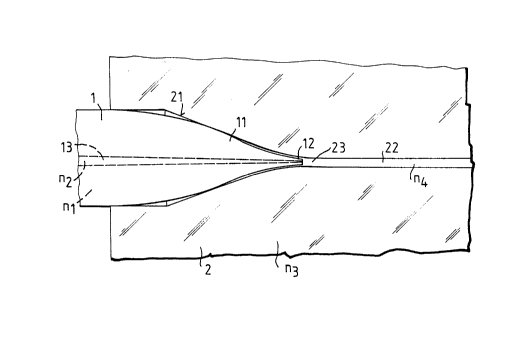
The basic structure of the coupling device is
shown in Figures 1 and 2. It consists of a glass fibre 1
having a core with an index of refraction n2, and having an
envelope surrounding the core 13 with an index of refraction
of n1, where n1 < n2. The glass fibre 1 has a tapered zone
11 and a tip 12. The coupling device also consists of a
substrate 2 of an integrated optical circuit, that substrate
having an index of refraction n3. It further consists of a
waveguide 22 having an index of refraction n4, and a fibre-
receiving portion 21 in the substrate 2. The tip 12 of
tapered glass fibre 1 has a diameter in the order of common
core dimensions of dielectric waveguides, so as to permit a
very close approach to the end 23 of the waveguide 22.
Fibre-receiving portion 21 need not necessarily
have the V-shape shown in Figure 2. Its shape need only be
sufficient to guide the glass fibre 1 during insertion, and
to secure it in an accurate position when inserted. In
order to guarantee field guiding in the area of the tip 12,
the effective index of refraction n3eff in the neighbourhood
of the tip 12 must be smaller than the index of refraction
n1 of the envelope surrounding the core 13 of glass fibre 1.
In the simplest case, this is achieved by using a substrate
material 2 that has an index of refraction n3 < n1. The
effective index of refraction n3eff can otherwise be adjusted
~i37g~!~
-
to the desired value by a corresponding diameter selection
of the fibre receiving portion 21.
The index of refraction n4 of the waveguide 22 has
to be larger than the index of refraction of the substrate
n3. Those index values and the waveguide cross-section are
matters that a person skilled in the art should be able to
choose such that the electromagnetic field distributions at
the tip 12 of glass fibre 1 and at the end 23 of waveguide
22 match as closely as possible. As can be demonstrated by
simulation calculations, an optimum value of the index of
refraction n4 of waveguide 22 is generally in the order of
the value n1.
It is advantageous to use an optically-transparent
polymer as the substrate 2 for several reasons. Firstly,
its index of refraction n3 can be easily adjusted to the
desired value. Secondly, the structure of fibre-receiving
portion 21 is achieved in a simple manner by the moulding of
a master structure through hot-pressing, injection moulding
or a similar process. For making a master structure, photo-
lithography, anisotropic etching and laser ablation arerecommended. Due to the multiple ways of moulding such a
master structure, its production expense is a minor factor,
and quite complicated structures can be formed.
If the shape reduction of the tapered zone 11 of
the glass fibre 1 is achieved by drawing under heat exposure
until breakage, a non-uniform, but repeatable, reduction in
diameter along the fibre axis will result --- as is shown in
~1379~9
-
Figure 1 and is known to those skilled in the art. Using
this shape has the advantage that the loss is less than that
from using the cone-shaped reduction shown in Figure 2.
Figure 3 illustrates a coupling device in which a
fibre-receiving portion 21 of a substrate 2 has a shape that
is adapted to receive the fibre-drawn profile of glass fibre
1. Unlike in Figure 1, the fibre-receiving portion 21 in
Figure 3 is configured as closely as possible to the fibre-
drawn profile of the glass fibre 1 in order to hold fibre 1
more securely and to minimize scattering losses.
The embodiment of Figure 4 has advantages in both
fibre entry guidance and mechanical stability. In this em-
bodiment, the integrated optical circuit includes not only
a substrate 2, but also a cover portion 3 which is generally
symmetrical to substrate 2 and in which a second part 31 of
the fibre-receiving portion is integrated.
This embodiment is particularly advantageous for
production if the waveguide structures in cover portion 3
and substrate 2 are configured as grooves during pressing/
injection moulding, and those grooves are filled up with a
suitable thermally-linkable or photochemically-linkable pre-
polymer. After assembly of cover portion 3 and substrate 2,
the glass fibre 1 is inserted into the receiving portion 21,
31. Finally, the core material of the waveguide is cured by
heat exposure or ultraviolet radiation, thereby gluing cover
portion 3, substrate 2 and glass fibre 1 together.
~137~39
A further advantageous embodiment of the coupling
device is shown in Figure 5. Here a gap 24 is deliberately
left between the end of the waveguide 22 and the tip 12 of
the glass fibre 1. After insertion of glass fibre 1, gap 24
is filled with a viscous, possibly curable, material having
a corresponding index of refraction to thereby achieve the
smallest possible coupling losses and back-scatter.