Note: Descriptions are shown in the official language in which they were submitted.
wo 94/0l8s6 2 1 ~ 8 6 ~ 4 PCr/US92/10009
.;.
. `
~,~ . .
~IIJL'rIPQ~T G ~Vl1~0~5
BACK~RC)UND OF THE INVENTION
This invention relates generally to controllers for v~deo gamAes and
simulators implemented on a computer and more particularly to interfacing
multiple multifunctional controllers to a personal computer.
Conventionally, a personal computer is enabled to be controlled by
external manual control de~rces by means of a game card, which provides
an exterrAal game port into which control dev~ces, s~lch as a joystick, c ar~A be
plugged. To provide w~despread compatibility, which is essential to the
ability to mass market a w~de variety of video games and simulation
programs, industTy standards have been developed for gamAe cards for
personal computers such as those coA~nonly referred to as IBM-
comApatibles. The un*ersal adoption of these standards means that any
exterrAal marAual input device designed to control such computers and
sof~ware must be compatible with the industry~standard game poArt. Any
input device lacking such compatibility will not be able to be used with
eonveA~ onal personal computers equipped with standard game boards and
2 o will not be widely accepted.
The problem is that the industry standard game poArt prov~des only a
limited number of inputs: four discrete signal irputs for receiving bi~ry
SigIlals signifying "On" and Of ~' and four analog signal inputs for receiving
Yariabie voltage signals, such as output by a potentiometer, which are
2 5 continuously variable over a limited range. The number of game boards
that can be plugged into a conventional PC is also limited, to one.
Consequently, the numAber of controllers supported by a stanAdard g~m e port,
arAd the number of allowable functions communicated thereby, is severely
restricted.
3 o For examAple, a PC configured as a combat aviation video
wo 94/01856 213 8 fi 5 4 PCI/US92/l0009
f
game/simulator as shown in FIG. 1 has a joystick controller and a foot-
pedal rudder controller. The joystick conventionally has a handle pivotally
coupled to a base for forward/rearward movement and left/right movement
by the user. The handle i~ connected in the base to transducers such as
5 potentiometers coupled to two of the analog inputs of the game port to input
proportional signals to the PC microprocessor to control analog functions in
the video game/simulation program. The handle also includes four discrete
switches that are operable by the user's fingers to control discrete fimctions
in the video game/simulation program. The joy-stick controller therefore
10 consumes two of the analog inputs and all four of the discrete inputs. The
foot-pedal rudder controller potentiometer can be supported on one of the
remaining analog inputs by providing a"Y-connector" as shown in FIG. 1,
which is known in the art. With this arrangement there are no discrete
inputs left in the conventional game port to support the discrete switches of
15 a throttle controller and only a single analog input.
Attemptingto circumventthese limitations, video g~rne and simulator
programmers have implemented maIly commands byprogramming function
keys on the PC keyboard. This approach detracts from the realism of
simulation, which is particularly important to flight simulation video
20 games. Developers have strived to attain more realism by designing
microprocessor-based input devices which output keycodes to the PC
keyboard port emulating function keys on the PC keyboard. One example
is disclosed in U.~. Pat. No. 4,852,031 to Brasington. Thrustmaster, Inc.
has also marketed a single throttle controller that outputs keycodes to the
2 5 PC keyboard port. These efforts have been successful to some extent but
have also encountered limits on the number of controllers that can be used
simultaneously.
In addition to the technical limitations of the keyboard emulation
technique, the cost and complexity of the electronics required to accomplish
3 0 the keyboard port emulation can also be prohibitively expensive. Because
21386~4
wo 94/018~6 PCr/Us92/10009
of the ubiquitous use of the controlled functions irl complex video games the
emulation hardware must be able to trzLnslate the controller inputs into one
of mc~my unique key commands required by the specific video simulalion
software. In order to accomplish the emulation, as well as provide the
5 normal keyboard fimctionalit~, the hardware typically requires a
microprocessor and its associated components, e.g., RAM c~nd ROM.
Other approaches to supporting additional inputs and/or controllers
are disclosed in the following U.S. Patents: No. 4,588,187 to Dell; No
4,924,216 to Lemg; No. 4,868,780 to Stern; No. 5,234,395 to Stern; cmd No
4,~01,424 to Stone et al. These are generally more complicated and
e~perlsi~e than is desirable.
Accordingly, a need remains for a be$ter way to interface a plurality
of m~ti-fimctional game controllers to a video game or simulation progr m
running on a conventional PC v~a a game card without having to emulate
keyboard commands in hardware.
SUMMARY OF THE INVENTION
~t is, therefore, an object of the invention to improve the ability of
personal computers to be controlled by multifi~ctional controllers at lower
cost.
2 0 Another object is to provide a video g~me controller interface which
can support at least two separate game controllers without the use of the
keyboard port.
A further object of the invention is to eliminate the need for a
keyboard or ~or keyboard emulation hardware that has, up to this point,
2 5 ~een required to support more that one multifunctional game controller.
The invention is an improvement in a video game controller interface
which provides supports for a plurality of game controllers via a game port
The invention maps input data from each of the plurality of g~me
controllers to unique addresses with;n the memory space of the personal
3 0 computer. A program operating on the computer selectively polls each of
wo 94/01856 2 1 3 8 ~ ~ 4 PCr/US92/lOOo9
the ~vailable address locations at which data from the individual controllers
can reside, to access the input signals from each ofthe controllers and apply
the inputs to the appropriate video game software functions. The program
includes a method of polling the individual game controllers to test for their
5 existence and, if detected, to receive individual input signals therefrom.
This invention enables the range of devices that caIl be supported
f~om a single video game port to be substantially increased without making
any change to the base computer hardware. The use of an inexpens*e
multiported game card, according to the present invention, and a mere
10 software change in the computer is all that is needed to make use of the
additional game controllers. This invention enables much more
sophisticated video games to be played successfully on a standard PC but is
not limited to game-playing. It can be used in other applications of personal
computers that make use of a game port or similarly limited input port,
15 such as in data logging system~.
The foregoing and other objects, features and advantages of the
invention will become more readily apparent from the following detailed
descnption of a preferred embodiment ofthe invention which proceeds with
reference to the accompanying drawings.
BRIEF DESCRIPTION OF THE DRAWINGS
FIG. 1 is a perspective view of a personal computer and keyboard with
two multifunctional game controllers connected according to the inventlon.
FIG. 2 is a block diagram of a dual port game board circuit in
2 5 accordance with invention connected to a conventional personal computer
input/output bus.
FIG. 3 is a schematic of the address decode circuitry of FIG. 2 used
to map the separate game ports to distinct memory ranges~
FIG. 4A is a perspective view of the back side of the split throttle
3 0 controller of FIG. 1.
~.i ., .
wo 94/018;~ 2 1 3 8 6 ~ 1 - P~tus92/10009
-
FIG. 4B is a perspective view of the front side of the split throttle
controller of FIG. 1.
FIG. S is a fimctional block diagram of the system of FIG. 1
incorporating at least two multifunctional controllers usi~g the dual port
5 game board of FIG. 2 and programming to utilize all outputs f~om the
controllers in a video game program.
FIG. 6 is a fiow chart of a subroutine for detecting multiple cont~ollers
in the system of FIG. 5.
FIG. 7 is a schemat;ic view of a first embodiment of a resistor ladder
10 network capable of combining multiple discrete switch inputs into a single
analog input.
FIG. 8 is a schematic view of a second embodiment of a resistor ladder
network capable of combining multiple discrete switch inputs into a single
analog input.
FIG. 9 is flow chart for an input control routine to be used in video
game or simulator software for interpreting analog inputs from the control
device of FIG. 7 and 8 in accordance with the invention.
DETAILED DESCR~TION
FIG. 1 shows a video g me/simulation system 10 for simulating
2 0 operation of a complex systemhavingapluralityofuser-cont~olledfunctio~s
such as a combat aviation video game progr~m. The system i~cludes a
conventional personal computer 12 ha~nng a microprocessor operable under
control of a video game/simulation program stored in memory, a
conven$ional display 14 for displaying images produced by operation of the
2 5 program in the microprocessor, and optionally a conventional keyboard 16.
Preferably, for running aviation video games and simulation
programs, both a split-throttle controller 18 and a joys$icl~ controller 20 are
connected to the computer, as well as a foot-pedal rudder controller 50. In
prior art video g~me systems, which have only a single game port, one or
30 more of the game controllers are connected to the keyboard port 26.
O 94/01856 2 1 3 8 6 '~ ~ ` PCI/US92/10009
f~
However, accordingto theinvention, the split-throttle controller 18 is shown
connected to a first game port 22 of a gam8 card 60 (FIG. 2) residing in the
housing of computer 12, and the joystick controller 20 and foot pedal rudder
controller 50 are connected via a "Y-conrlector" to a second game port 24
s located on the same game card. Only the keyboard 16 is connected to the
keyboard port 26.
As previously mentioned, the joystick controller 20 and foot-pedal
rudder controller 50 consume all four discrete inputs and three of the fou2
analog inputs of a conventional game port. A directional controller, or "joy
10 hat" 46, is also implemented using discrete switches to provide center,
forward, backward, left and right control positions. The discrete switches
are combined into a single analog input using a resistor ladder network as
descnbed herein below.
The split^throttle controller 18 shown in FIGS. 1, 4A and 4B itselfhas
15 an additional seven discrete switches 82, a three-way switch 86, three
potentiometer outputs, and a track ball 88. The three potentiometer
outputs, which transduce the positions of two throttle sticks 94 and 96 and
the position of a rotary dial 84 mounted on the throttle, consume three
analog inputs. The switches alone cannot be supported by only the four
2 o discrete inputs of a conventional game port, not to mention the other inputs.
- The discrete switches are combined with the three-way switch into a singie
analog input using a resistor ladder network as described below. By
co~nbining the discrete in?uts into a single analog input, the split-throttle
controller 18 is able to include a track ball 88 operated by the thumb for
2 5 positioning a cursor on the screen during the video simulation. The track
ball output circuitry consumes all four ofthe discrete inputs to represent the
four directions of movement: right, left, up, and down. Trackballs providing
four discrete outputs for representing the relative movement of the ball are
comm~rcially available, such as the F13 Tracking Mechanism by Appoint,
3 0 Inc. However, it may be necessary to buffer the discrete outputs ofthe track
21~865~
WO 94/01856 PCI/~S92/10009
I
b~ll depending on the olltput drive characteristics of the track ball selected.
The joystick 20, the foot-pedal rudder controller 50, and the split-throt~le 18
require two separate and complete game ports to support all of the input
capability of the controllers, but conventional PCs only support one single-
5 port game card.
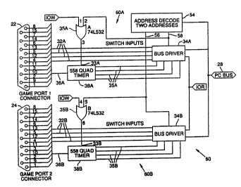
As shown in FIG. 2, two game ports 22 and 24 are selectivelyconnected to a PC input/output bus 28 of a multi-ported game board 60,
described in detail below. Not expressly shown in FIG. 2 are the support
components such as pull-uplpull-down andlor series resistors and capacitors
0 that would be reqwred in a commercially available product, the use of which
are commonly known in the art of digital design. The PC I/O bus 28 is
conventionally provided in computer 12 for connecting peripheral input and
output devices to the PC microprocessor. The PC bus consists of a data bus,
over which data is passed to and from the microprocessor, and a ~ontrol bus,
15 over which the address and control signals are transmitted to control
peripheral devices residing on th2 bus. Two ofthe control signals are shown
explicitly: the write strobe IOW, which indicates a valid microprocessor
write cycle; and the read strobe IOR, which indicates a valid microprocessor
read cycle. The use of these two signals in the invention vrill become
2 0 apparentthrough the detailed description ofthe preferred embodiment that
follows.
Conventionally, the game board coupled to the PC bus 28 has a finite
number of inputs for receiving and inputting to the microprocessor a limited
number of discrete and analog input signals through a single industry
2 5 standard game port connector, as stated above. This embodiment provides
two such con~ectors 22,24, for coupling at least two multifi~nc~onal
controllers to game port interface circuits 60A, 60B. Each of the game port
interfaces 60A,60B has four binary or discrete switch inputs ~2A and 32B
and four analog inputs 36A,36B. In order for the analog inputs to be read
3 0 over the microprocessor data bus? the variable analoginputs are converted
wo 9¢/01856 2 1 3 8 6 5 4 PCI'/llJS~2/10009
to a digital signal having a width proportional to the Yoltage of the signal by
a quad timer 38A,38B. The quad timer samples each of its respective
analog input signals responsive to a trigger pulse received an its trigger
input 33A,33B. The quad timer includes a o~e shot circuit that receives
variable voltage level signals f~om the respective game port connector 22 or
24 and outputs constant level signals of a duration proportional to input
voltage level.
The microprocessor reads the discrete inputs and the quad timer
outputs of one of the game ports 22 or 24 one at a ~me, according to the
inventive principle, and outputs the signals to the PC DUS 28 via the
corresponding bus driver 34A or 34B. A subrou~ne within the video
game/simulation program, after issuing the tsigger command, times the
di~erent duration signals and selects a unique control command in the
program in accordance with the timed duration. In this way, the personal
computer is able to sense the magnitude and direction of the variable input
signals to effect a corresponding change in the displayed images produced
by the program. The use of the timer to convert continuously va iable
analog inputs to proportional duration digital signals is known in the art of
game board design.
2 o In order to differentiate between the two game ports 22, 24, the game
board circuitry includes a strappable address decode circuit 54. The major
constituent parts of the circuitry are shown in greater detail in FIG. 3.
The address decodermonitors the PC bus for the unique addresses assigned
to the game card ports and selectively enables the respective game port
2 s when the valid address is received. Conventionally, the game port resides
at the 0201H address, as shown in "Interfacing to the IBM Personal
Computer", pp. 197-198, by Lewis C. Eggebrecht (1983). However, the
remainder of the address loca~ons within the 0200H-0277H contiguous
address range are unused, as shown by Eggebrecht (1983), pg. 129. The
3 0 purpose of the memory map logic 62 is to decode a portion of the unused
21386~4
wo 94/018~6 ~ PCr/US92/l0009
address space, including 0201H, hereafter known as the game port address
space, and issue a valid enable signal 76 when a valid microprocessor bus
access to the game port address space is detected. The enable signal 76
drives the enable input of a conventional 3-to-8 decoder 64, e.g., 74LS138.
The select inputs 70,70,74 of the decoder are driven by the least significant
address bits ofthe PC control bus, which in turn specify the precise ad~ress
within the game port address space currentlybeing addressed. The outputs
of the decoder then correspond to a unique address within the game port
address space.
The outputs of the decoder are grouped into two separate groups of
sigIlal lines 78 and 80. The first group of signal lines 78 correspond to the
first four outputs of the decoder, and the last group of signal lines 80 to the
last four outputs of the decoder. The first group of signal lines 78 are
coupled to the inputs of a first jumper block 66. The jumper block consists
of four individual input posts and four corresponding output posts. The
input posts are connected to the corresponding output posts by mounting a
jumper across the t~vo posts. The jumpers are individually removable. The
outputs ofthe first jumper block are coupled together to form the first game
port enable signal 58. By mounting a jumper on the jumper block the
2 0 specific address of the first game port 22 can be selectively mapped to any
of the four addresses of the first group of signals. Moreover, more than one
jumper can be inserted, resulting in the first game port 22 being mapped to
the corresponding multiple addresses. Similarly, the second group of
signals 80 are coupled to a second jumperblock 68, the outputs of which are
2 S tied together to form the second game port enable signal 56. A dual-in-line
package (DIP) switch can be substituted for the jumper blocks.
Referring back to FIG. 2, the output signals 56, 58 produced by the
address decoder ~re combined with the read and write strobes, i.e., IOR
and IOW, to either selectively enable the corresponding bus driver 34A,
3 0 34B during a read, or selectively trigger the selected quad timer one-shot
wo 94/01856 2 1 3 8 6 ~5 ~ ~ PCr~US92/lOoO9
~ .
du~ng a write. For a read, the selected output signal ~6, 58 is combined
with the read strobe IOR through an OR gate 35A, 35B, ~Ihich acts as a
negative AND gate with active low inputs and outputs. For a write, the
selected output signal is combined with the write strobe IOW by the bus
5 driver 34A, 34B by providing separate enable inputs for the write strobe
IOW and the selected output signal 56, 68. The combination ofthese signals
is known in the art of digital logic and may take on different fo~s
depending on the logic available to the designer, e.g., programmable logic
devices.
Referring to FIG. 5, a functional block diagram of the system of FIG.
1 is shown incorporating at least two multifunctional controllers 18, 20
using the dual port game board of FIG. 2 and programming to utilize all
outputs from the controllers in a video game program. The outputs of the
joystick controller 20 and the foot-pedal rudder controller 50 are selectively
15 output through the first game port interface 60A onto the PC I/O bus 28
respons*e to the control signals of microprocessor 98 operable under the
control of either the video game software (S/W) 100 or a so-called termiIlate-
and-stay-resident (T.S.R.) ~3fW 102 program, as desc~ibed in detail below.
Similarly, the outputs of the split throttle controller 18 are selectively
2 o output through the second game port interface 60B onto the PC I/O bus 28.
The microprocessor receives the data over the PC I/O bus 28 and places the
da~a in either the first address space 104 corresponding to the video game
software 100, or the second address space 106 corresponding to T.S.R. S/W
102. The video game S/W 100 then receives the data input and updates the
2 5 cathode-ray-tube (CRT) display 14 according to the data input sti~nulus.
Within the computer, an input sub-rout~e, which can be either the
T.S.R. progr~m 102 or an integral part of the video simulation program
100, as mentioned above, vvill selectively poll the assigned addresses to
receive the input data received from each of the controllers, after detecting
3 0 the presence of one or more controllers. Refemng to FIG. 6, the program
wo 94/01 856 21~ 8 6 5 4 pcr/uss2/1 ooos
11
detects the presence of the controllers by executing the following
initialization sequence for each of the controllers: writing to the individual
timer port 108; waiting 8 period oftime greater than that possibly produced
by a valid voltage level on the analog inputs 110; and reading the
5 corresponding digital output to determine whether a transitiorl occurred on
the individual analog inputs 144; and setting a flag to indicate the presence
ofthe controller 118, or the lack thereof 116, dependent on the whether the
level of ~he timer output is low or high 114, respectively. The sa_e
sequence is followed to determine the presence of the second controller, as
shown in steps 120-130 of FIG. 6.
Once the controller's presence is determined, the input subroutine
continuously polls the indi~idual controller addresses in a predetermined
marmer, e.g., round-robin to monitor for new input. In the case ofthe T.S.R.
102, the subroutine will act as a keyboard emulation progr~m by recei~ing
15 input signals from each of the separate controllers and placing the
corresponding key~oard sequence in the keyboard input buffer, i.e., the
second address space 106, for receipt by the simulation program.
Alternatively, the input subroutine is integrated into the simulation
progr~m. The subroutine then polls each of controllers individually to
2 0 rece*e input signals therefrom and place it directly in the video game S/W
100 address space, i.e., the first address space 104, and take the
corresponding action dictated by the input without translating the input
into a keyboard sequence.
For example, in a combat aviation video g~me the joystick controller
5 20 is used to control the direction of the combat aircraft. The movement of
the joystick handle changes the two potentiometer settings 40 corresponding
to the left/right and up/down movement. Periodically, the video g~me
software 100 or the T.S.R. 102 will poll the corresponding game port to
check for new input stimulus received over the game ports. In the case of
3 0 input data received from the joystick, the soflcware will begin timing the
wo 94/018~6 213 8 ~ 5 A PCr/US92/lo009 ~ `
~, I
12
pulse width of the timer outputs corresponding to the joystick poten~ometer
to determine the exact position of the joy~tick, either left or right, or up or
down, or a combination of both. Once the timer pulses have elapsed, the
video ga~ne software 100 updates the CRT 14 to reflect the new viewing
5 angle dictated by the joystick handle position.
Similarly, input signals from the split-throttle controller 18 are
translated into commands for other aspects of the avia~on program.
Although the anation program allows for the input signals to be
programmed to a variety of control functions, one possible configuration for
the split-throttle 18 is as follows. Ihe two individual throttle members 907
92 provide two separate analog input commands to control the left and right
engines of a multiengine combat aircraft. The track ball 88 uses the four
discrete irlputs to move a cllrsor on a radar screen displayed on the CRT 14
to selectindividual targets. The plurality of individual discrete switches 82
15 mounted on the throttle members, in conjunction with the three-way switch
86, input control signals through the third analog input for a variety of
con~ol fi~ctions used to simulate air-to-air combat such as target select,
target lock and unlock, etc. In addition, the rotary dial 84 uses the fourth
analoginput to control the antenna eleva~on. In this way, by operating the
20 joystick and the split-throttle simultaneously, as well as the foot-pedal
rudder controller, the operator feels as if he is operating a true combat
aircraft in a real time combat situation.
Referring now to FIG. 7, as mentioned above, in order to support more
discrete switches than the number of available discrete inputs on the game
25 board, the individual switches S1, S2,... Sn are combined into ~ single
analog input 36 through a resistor ladder network. All of the individual
switches S1, S2,... Sn are coupled between a common voltage source Vin
and one of the analog output signal lines through a different impedance so
as to produce a di~ferent discrete voltage level of signal Vout on the analog
3 0 output signal line uni~uely corresponding to actuation of each switch.
~ , . . , .~
.~ . . . . . . . . . . . . - . . ~ . . ~ . . ,
wo s~/018s6 2 1 ~ 8 6 ~ 4 PCr/Us9~/10~09
~ I
13
FIG. 7 shows a switch circuit arranged so that each switch 51, S2,...
Sn is connected in series with a resistor to form a single switching subcircuit
and all of the switching subcircuits are connected between the common
input voltage node and a single output node coupled to said one analog
5 output signal line. In this circuit it is preferred ~or each resistor to have a
di~ferent value of resistance.
FIG. 8 shows a switch circuit arranged in a ladder circuit with the
switches S1, S2,... Sn connected between the common input node and a
series at output nodes coupled in series by separate resistors to a single
10 output node coupled to said one analog output signal line. In this ~rcuit it
is pre~erred for each resistor to have the same value of resistance.
The game board timer 38 converts the dif~erent discrete signal levels
on the analog output signal line 38 into dif~erent duration signals. A
su~routine, shownin FIG. 9, is added to the video game/simulation program
15 for timing the dif~erent duration signals and selecting a unique control
command in the progr~m in accordance with the timed duration. In tbis
way, the personal computer interprets each dif~erent discrete level of signal
as a separate discrete command and inputs such command to the video
game/simulation program to effect a corresponding change in the displayed
2 0 images produced by the program.
Having described and illustrated the principles of the invention in a
preferred embodiment thereof, it should be apparent that the invention can
be modified in arrangeme~t and detail without departing from such
principles. For example, is should be apparent that the number of game
2 5 ports can be increased by assigning smaller address ranges to each of the
game ports. The number of game ports being limited by the physical space
of the connectors and/or the number of unique addresses available. I claim
all such modifications and variation coming within the spirit and scope of
the following claims.
... . .... .. .. . .. . .. .. . .. . . .