Note: Descriptions are shown in the official language in which they were submitted.
2138730
Clock Signal Regeneration Method and Apparatus
BACKGROUND OF THE INVENTION
1. Field of the Invention
This invention relates to a clock signal
regeneration method and apparatus for regenerating a
clock signal synchronized with received data, and more
particularly to a clock signal regeneration method and
apparatus for use in the field of digital radio
communications wherein, from received data, a timing
signal corresponding to the rate of the received data is
extracted and compared in phase with a regenerated clock
signal outputted from the clock signal regeneration
apparatus to produce a phase difference signal
corresponding to the difference in phase between the
timing signal and the regenerated clock signal and then
the phase of the regenerated clock signal is corrected
based on the phase difference signal.
2. Description of the Related Art
Such a clock signal regeneration apparatus as
shown in FIG. 8 is conventionally known as a clock
signal regeneration apparatus which employs a phase
locked loop (PLL). Referring to FIG. 8, the clock
2138730
signal regeneration apparatus shown includes a timing
extraction circuit 101 for extracting, from received
data, a timing signal corresponding to the rate of the
received data, a phase comparator 102 for comparing the
phases of the timing signal extracted by the timing
extraction circuit 101 and a regenerated clock signal
outputted from the clock signal regeneration apparatus
with each other and outputting a phase difference signal
of a voltage corresponding to the phase difference, a
loop filter (low-pass filter) 103 for removing high
frequency components from the phase difference signal
from the phase comparator 102, an addition/subtraction
control circuit 104, a count value correction circuit
105, and a counter 106 for counting pulses of a
controlling clock signal (FAST CLOCK) having a frequency
N times that of the timing signal.
The addition/subtraction control circuit 104
outputs, in response to a phase difference voltage
outputted from the loop filter 103, a signal indicating
whether the count value of the counter 106 should be
incremented or decremented by one. The count value
correction circuit 105 corrects the current count value
of the counter 106 in response to the output of the
addition/subtraction control circuit 104 and loads the
2138730
thus corrected count value into the counter 106 in
response to the regenerated clock signal of the clock
signal regeneration apparatus.
By the operation just described, the counter 106
modifies its count value in accordance with a phase
difference between the timing signal extracted from the
received data and the regenerated clock signal, and
controls the phase of the regenerated clock signal with
a step equal to 1/N of the step at the data rate of the
received data. This operation plays the role of a
voltage controlled oscillator (VC0) of a PLL circuit so
that a clock signal corresponding to the rate of the
received data is regenerated.
The phase control of the regenerated clock
signal of the conventional apparatus described above,
however, has an upper limit defined by the width of one
clock of the controlling clock signal and only allows
phase control in minimum units of the thus limited fixed
width. In particular, where the controlling clock
signal has a rate equal to N times the data rate, the
phase of the regenerated clock signal cannot be
corrected with a step smaller than 1/N of the step at
the data rate. This relationship is illustrated in a
time chart of FIG. 9. Referring to FIG. 9, where the
2138730
data are such as illustrated by the curve (1), the curve
(2) illustrates a regenerated clock signal which is
displaced in phase from the data signal by an amount
equal to a minimum phase control width a of one step
while the curve (3) illustrates another regenerated
clock signal which is corrected optimally in phase. In
this instance, the minimum phase control width a is
equal to 1/N of the width of one symbol of the data, or
in other words, equal to the width of one clock of the
controlling clock signal.
Accordingly, in a system in which a large amount
of data is processed at a high speed, when the rate of
data is so high that the ratio "N" between the symbol
rate o~ the data (the symbol rate signifies the number
of symbols which can be transmitted within one second;
the symbol rate is equal to the bit rate where the data
are binary digital modulation data, but is equal to 1/2
the bit rate where the data are four-value digital
modulation data) and the rate of the controlling clock
signal cannot be set high, the regenerated clock signal
exhibits high phase jitters, and consequently, a high
performance of the system cannot be assured. Further,
if it is intended to suppress the phase jitters of the
regenerated clock signal, then the frequency of the
2138730
controlling clock signal must be set extremely high.
For example, if it is tried to suppress phase jitters
within 3~ with the data rate of 2.5 Mb/s, then the
frequency of the controlling clock signal must be 300
MHz or more. This value is not actually practical.
SUMMARY OF THE INVE~TION
It is an ob;ect of the present invention to
provide a clock signal regeneration method and a clock
signal regeneration apparatus by which phase control of
a regenerated clock signal can be performed at a step
smaller than the width of one clock of a controlling
clock signal to improve the accuracy in rate of the
regenerated clock signal to reduce phase jitters readily
even with a high speed system.
In order to attain the object described above,
according to an aspect of the present invention, there
is provided a clock signal regeneration method for
regenerating a clock signal synchronized with received
data, which comprises the steps of extracting, from the
received data, a timing signal corresponding to a rate
of the received data, comparing the phases of the thus
extracted timing signal and a regenerated clock signal
with each other to produce a phase difference signal
2138730
corresponding to the phase difference between the timing
signal and the regenerated clock signal, repetitively
adding the phase difference signal at each clock of the
regenerated clock signal in a cycle of a controlling
clock signal whose frequency is higher than that of the
timing signal to produce a phase difference integrated
value for each of such adding operation, converting the
phase difference integrated value into amplitude
information by which an amplitude of a sine waveform is
represented in a digital value, converting the amplitude
information into an analog signal, and comparing the
analog signal with a reference voltage to produce a new
regenerated clock signal to be outputted as a
regenerated clock signal and to be used at the first
comparing step in a next cycle.
Preferably, at the repetitively adding step, a
predetermined bias value is added to the phase
difference signal.
Amplitude information in which amplitudes of the
sine waveform are represented in digital values may be
stored in advance in storage means, and the amplitude
information may be read out from the storage means
designating the phase difference integrated value as a
read address for the storage means.
2138730
Preferably, high frequency components are
removed from the phase difference signal obtained at the
first comparing step, and high frequency components are
removed from the analog signal obtained at the second
converting step.
According to another aspect of the present
invention, there is provided a clock signal regeneration
apparatus for regenerating a clock signal synchronized
with received data, which comprises a timing extraction
circuit for extracting, from the received data, a timing
signal corresponding to a rate of the received data, a
phase comparator for comparing the phases of the timing
signal extracted by the timing extraction circuit and a
regenerated clock signal with each other to produce a
phase difference signal corresponding to the phase
difference between the timing signal and the regenerated
clock signal, integration means for repetitively adding
the phase difference signal at each clock of the
regenerated clock signal in a cycle of a controlling
clock signal whose frequency is higher than that of the
timing signal to produce a phase difference integrated
value for each of such adding operation, amplitude
information conversion means for converting the phase
difference integrated value into amplitude information
2~387~0
by which an amplitude of a sine waveform is represented
in a digital value, digital to analog conversion means
for converting the amplitude information into an analog
signal, and waveform shaping means for comparing the
analog signal with a reference voltage to produce a new
regenerated clock signal to be outputted as a
regenerated clock signal from the clock signal
regeneration apparatus and to be supplied to the phase
comparator.
With the clock signal regeneration method and
apparatus, where the frequency of the controlling clock
signal is equal to N times that of the timing signal
extracted from the received data, the phase difference
signal for each clock of the regenerated clock signal is
repetitively added at a rate equal to N times that of
the timing signal to obtain a phase difference
integrated value for each of such adding operation. The
phase difference integration value is incremented by a
value corresponding to the phase difference in a cycle
equal to 1/N of the cycle of the received data, that is,
equal to one cycle of the controlling clock signal, and
for each phase difference integrated value, the
amplitude of the sine waveform is converted into
amplitude information represented in a digital value.
2 ~
The amplitude information is converted into an
analog signal, and the analog signal is compared with a
reference voltage to shape it by waveform shaping thereby to
obtain a new regenerated clock signal which has been corrected
in phase. While also the amplitude information is obtained in
the same cycle as that of the controlling clock signal, since
the phase of the regenerated clock signal obtained newly is
based on the analog signal obtained by converting a digital
value of the amplitude of the sine waveform into an analog
value by digital to analog conversion, the phase control width
of one step is not fixed to a value whose minimum limit is 1/N
of the cycle of the controlling clock signal as in
conventional clock signal regeneration apparatus, but can be
varied at a smaller step than 1/N of the cycle.
In accordance with the present invention there is
provided a clock signal regeneration method for producing a
regenerated clock signal synchronized with digitally modulated
received data, comprising the steps of: extracting, from the
digitally modulated received data, a timing signal
corresponding to a rate of the digitally modulated received
data; comparing a phase of the timing signal with a phase of
the regenerated clock signal to produce a phase difference
signal corresponding to phase difference between the timing
signal and the regenerated clock signal at each clock of the
regenerated clock signal; repetitively adding the phase
difference signal at said each clock of the regenerated clock
signal in a cycle equal to 1/N times a cycle of the timlng
signal with a controlli-ng clock signal whose frequency is
76733-5
equal to N times that of the timing signal to produce a phase
difference integrated value for each of such adding operation,
wherein N is an integer: converting the phase difference
integrated value into amplltude information by which an
amplitude of a sine waveform is represented by a digital
value; converting the amplitude information into an analog
signal having a varying sine waveform; and comparing the
analog signal with a reference voltage to produce a new
regenerated clock signal having a phase which varies by a step
size smaller than the 1/N times the cycle of the timing
signal, said new regenerated clock signal to be outputted as
the regenerated clock signal and to be used at the first
comparing step in a next cycle.
In accordance with the present invention there is
further provided a clock signal regeneration apparatus for
producing a regenerated clock signal synchronized with
digitally modulated received data, comprising: timing signal
extraction means for extracting, from the digitally modulated
received data, a timing signal corresponding to a rate of the
digitally modulated received data; phase comparison means for
comparing a phase of the timing signal with a phase of the
regenerated clock signal to produce a phase difference signal
corresponding to a phase difference between the timing signal
and the regenerated clock signal at each clock of the
regenerated clock signal; phase difference integration means
for repetitively adding the phase difference signal at said
each clock of the regenerated clock signal in a cycle equal to
1/N times a cycle of the timing signal with a controlling
9a
76733-5
Q f~'
clock signal whose frequency is equal to N times that.of the
timing signal to produce a phase difference signal integrated
value for each of such adding operation, wherein N is an
integer; amplitude information conversion means for converting
the phase difference integrated value into amplitude
information by which an amplitude of a sine waveform is
represented by a digital value; digital to analog conversion
means for converting the amplitude information into an analog
signal having a varying sine waveform; and waveform shaping
means for comparing the analog signal with a reference voltage
to produce a new regenerated clock signal having a phase which
varies by a step size smaller than the 1/N times the cycle of
the timing signal, said new regenerated clock signal to be
outputted as the regenerated clock signal and to be supplied
to said phase comparison means in a next cycle.
In accordance with the present invention there is
further provided a clock signal regeneration apparatus for
producing a regenerated clock signal synchronized with
digitally modulated received data comprising: a timing
extraction circuit configured to extract from the digitally
modulated received data a timing signal corresponding to a
rate of the digitally modulated received data; a phase
comparator configured to receive the timing signal from the
timing extraction circuit and the regenerated clock signal,
said phase comparator operable to compare a phase of the
timing signal with a phase of the regenerated clock signal and
to produce a phase difference signal corresponding to a phase
difference between the timing signal and the regenerated clock
9b
76733-5
7 3 ~ ~
signal at each clock of the regenerated clock signal; a phase
difference integration circuit configured to receive the phase
difference signal from the phase comparator and a controlling
clock signal said phase difference integration circuit
operable to repetitively add the phase difference signal at
said each clock of the regenerated clock signal in a cycle
equal to l/N times a cycle of the timing signal with the
controlling clock signal whose frequency is equal to N times
that of the timing signal to produce a phase difference signal
integrated value for each of such adding operation wherein N
is an integer; an amplitude information conversion circuit
configured to receive the phase difference signal integrated
value from the phase difference integration circuit and the
controlling clock signal said amplitude information conversion
circuit operable to convert the phase difference signal
integrated value into amplitude information by which an
amplitude of a sine waveform is represented by a digital
value; a digital to analog convertor configured to receive the
amplitude information from the amplitude information
conversion circuit and the controlling clock signal, said
digital to analog converter operable to convert the amplitude
information into an analog signal having a varying sine
waveform; and a waveform shaping circuit configured to receive
the analog signal from the digital to analog converter and a
reference voltage, said waveform shaping circuit operable to
compare the analog signal with the reference voltage to
produce a new regenerated clock signal having a phase which
varies by a step size smaller than the 1/N times the cycle of
~ 9c
,_~ 76733-5
3 ~ ;~
the timing signal, said new regenerated clock signal to be
outputted as the regenerated clock slgnal and to be supplled
to said phase comparator in the next cycle.
The above and other ob~ects, features and advantages
of the present lnventlon wlll become apparent from the
followlng description and the appended clalms, taken ln
con~unctlon wlth the accompanylng drawlngs ln whlch llke parts
or elements are denoted by llke reference characters.
BRIEF DESCRIPTION OF THF DRAWINGS
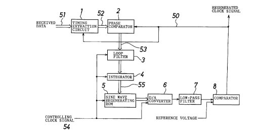
FIG. 1 ls a block dlagram of a clock slgnal
9d
- 76733-5
~138730
regeneration apparatus showing a preferred embodiment of
the present invention;
FIG. 2 is a block diagram showing exemplary
circuit constructions of a timing extraction circuit and
a phase comparator of the clock signal regeneration
apparatus of FIG. 1;
FIG. 3 is a time chart illustrating operation of
the timing extraction circuit and the phase comparator
shown in FIG. 2;
FIG. 4 is a block diagram showing an exemplary
circuit construction of an integrator of the clock
signal regeneration apparatus of FIG. 1;
FIG. 5 is a time chart illustrating output
waveforms of the integrator, a D/A converter, a low-pass
filter and a comparator of the clock signal regeneration
apparatus of FIG. 1;
FIG. 6 is a diagrammatic view illustrating the
relationship between an integrating operation of the
integrator of FIG. 4 and an address of a sine wave
regeneration ROM designated by the output of the
integrator;
FIG. 7 is a diagrammatic view illustrating a
read address of the sine wave regeneration ROM and a
sampling output with respect to a sine waveform;
--10--
~138730
FIG. 8 is a block diagram showing a conventional
clock signal regeneration apparatus; and
FIG. 9 is a time chart illustrating a limit in
phase control for a regenerated clock signal of the
conventional clock signal regeneration apparatus shown
in FIG. 8.
DESCRIPTION OF THE PREFERRED EMBODIMENT
Referring first to FIG. 1, there is shown a
clock signal regeneration apparatus to which the present
invention is applied. Referring to FIG. 1, the clock
signal regeneration apparatus shown includes a timing
extraction circuit 1, a phase comparator 2, a loop
filter tlow-pass filter) 3, an integrator 4, a sine wave
regenerating ROM 5, a digital to analog (D/A) converter
6, a low-pass filter 7 and a comparator 8. The clock
signal regeneration apparatus has the construction of a
PLL circuit wherein the output of the comparator 8 is
fed back as a regenerated clock signal 50 to the phase
comparator 2.
The timing extraction circuit 1 extracts, from
received data 51 in the form of a digitally modulated
signal, a timing signal 52 corresponding to the rate of
the received data 51. The phase comparator 2 compares
2138730
the phases of the timing signal 52 from the timing
extraction circuit 1 and the regenerated clock signal 50
with each other and outputs a phase difference signal 53
of a voltage corresponding to the phase difference
between the timing signal 52 and the regenerated clock
signal 50. Exemplary circuit constructions of the
timing extraction circuit 1 and the phase comparator 2
are shown in FIG. 2, and operations of components of
them are illustrated in FIG. 3, in which the received
data 51 are indicated in a waveform after D/A conversion
and in another waveform after removal of high frequency
components from the analog waveform.
Referring to FIG. 2, the timing extraction
circuit 1 includes a flip-flop circuit 201 to which the
received data 51 are inputted, another flip-flop circuit
202 for receiving the output of the flip-flop circuit
201, an invertor 203 for inverting the regenerated clock
signal 50, a further flip-flop circuit 204 for receiving
a most significant bit (MSB) of the received data 51,
and a still further flip-flop circuit 205 for
receiving the output of the flip-flop circuit 204. The
regenerated clock signal 50 is inputted as it is to the
flip-flop circuits 202, 204 and 205 while the output of
the invertor 203 which inverts the regenerated clock
-12-
2138730
signal 50 is inputted to the flip-flop circuit 201.
The phase comparator 2 includes an exelusive OR
circuit 207 for reeeiving the output of the flip-flop
cireuit 204 and the output of the flip-flop cireuit 205,
another exelusive OR (EXOR) circuit 206 for receiving
the output of the flip-flop circuit 202 and the inverted
output of the flip-flop circuit 205, and a selection
cireuit 208 for selecting the output of the exclusive OR
eireuit 206 in response to the output of the exclusive
OR eireuit 207.
Referring also to FIG. 3, the flip-flop eireuit
201 extraets the reeeived data 51 at a rising edge of
the output of the invertor 203 whieh inverts the
regenerated elock signal 50, and provides, if the data
then are displaced from the zero cross point, an output
having a positive or negative polarity corresponding to
the direetion of the displaeement and an amplitude
corresponding to the magnitude of the displacement. The
flip-flop circuit 202 delays the output of the flip-flop
circuit 201 by an amount equal to the ~idth of 1/2 clock
of the regenerated clock signal. The flip-flop circuit
204 extraets a variation of the MSB of the reeeived data
51 at a rising edge of the regenerated cloek signal 50.
The flip-flop eireuit 205 delays the output of the flip-
-13-
~138730
flop circuit 204 to a next rising edge of the
regenerated clock signal 50. The exclusive OR circuit
206 exclusively ORs the output of the flip-flop circuit
202 and the inverted output of the flip-flop circuit 205
to control the output of the flip-flop circuit 205 to
one of the positive and negative polarities. The
exclusive OR circuit 207 exclusively ORs the output of
the flip-flop circuit 204 and the output of the flip-
flop circuit 205 and inputs a resulted output signal to
the selection circuit 208. The selection circuit 208
selects the output of the exclusive OR circuit 206 when
the output of the exclusive OR circuit 206 crosses zero,
but selects zero when the output of the exclusive OR
circuit 206 does not cross zero, and outputs the selected
value as a phase difference signal 53. The phase
difference signal 53 exhibits a voltage according to a
phase difference having a negative value when the phase
of the regenerated clock signal 50 leads the phase of
the received data 51 but having a positive value when
the phase of the regenerated clock signal 50 lags the
phase of the received data 51.
Referring back to FIG. 1, the loop filter 3
removes high frequency components from the phase
difference signal 53 which is outputted from the phase
2138730
comparator 2 at each clock of the regenerated clock
signal. The integrator 4 repetitively or cumulatively
adds the phase different signal, from which high
frequency components have been removed by the loop
filter 3, in a cycle of a controlling clock signal 54 of
a frequency equal to N times that of the timing signal,
and outputs a phase difference integrated value 55 for
each such adding operation. An exemplary circuit
construction of the integrator 4 is shown in FIG. 4.
Referring to FIG. 4, the integrator 4 shown
includes two first and second addition circuits 301 and
302 and a single flip-flop circuit 303. The first
addition circuit 301 adds a predetermined bias value ~B
to the phase difference signal 53 outputted from the
loop filter 3 and outputs a resulted value to the second
addition circuit 302. The flip-flop circuit 303 delays
the output of the second addition circuit 302 by an
amount equal to the width of one clock of the
controlling clock signal 54 and outputs the delayed
signal back to the second addition circuit 302. The
second addition circuit 302 adds the thus inputted
output of the flip-flop circuit 303 and the phase
difference signal to which the bias value ~B has been
added by the first addition circuit 301. In other
-15-
~38730
words, the second addition circuit 302 repetitively adds
the phase difference signal, to which the bias value ~B
has been added, in a cycle of 1/N of the cycle at the
data rate and outputs a result of each such adding
operation as a phase difference integrated value 55 of
the integrator 4 as seen from the time chart of FIG. 5.
The phase difference integrated value 55 outputted in a
cycle of 1/N of the cycle at the data rate is provided
as a read address signal to the sine wave regenerating
ROM 5. Here, if the address of the sine wave
regenerating ROM 5 has, for example, an 8-bit
configuration, only lower 8 bits of the phase difference
integrated value 55 which is the output of the
integrator 4 are referred to so that address designation
may be performed repetitively in one cycle within which
addresses beginning with the first address at which all
of the eight bits are equal to "O" and ending with the
last address at which all of the eight bits are equal to
"1 " .
The sine wave regenerating ROM 5 stores in
advance amplitudes of a sine waveform as table data of
digital values. The sine wave regenerating ROM 5
receives the phase difference integrated value 55 from
the integrator 4 as a read address signal as described
-16-
21387~0
above and outputs sample data of the sine waveform
corresponding to the address. Such reading out
operation from the sine wave regenerating ROM 5 is
synchronized with the controlling clock signal 54, but
the maximum reading out rate is 1/N of the rate of the
controlling clock signal 54. However, since the sample
data of the sine waveform outputted from the sine wave
regenerating ROM 5 are controlled in phase by a
resolution corresponding to the bit length of the
address of the sine wave regenerating ROM 5, the phase
can be varied at a finer step than the step at 1/N of
the rate of the controlling clock signal 54.
FIG. 6 illustrates the relationship between the
integrating operation of the integrator 4 and the
address of the sine wave regenerating ROM 5 designated
by the output of the integrator 4. The read address for
the sine wave regenerating ROM 5 is incremented by a
value equal to the sum of the phase difference signal 53
and the bias value ~B.
FIG. 7 illustrates the relationship of the read
address and the sampling output of the sine wave
regenerating ROM 5 to the sine waveform. The read
address and the sampling output are represented in 8
bits, and amplitude information is stored for addresses
-17-
2138730
between the address where all of the 8 bits of the read
address are "O" and the address where all of the 8 bits
of the read address are "1", thereby constituting one
cycle of the sine wave. The sampling output
corresponding to the sine waveform exhibits a maximum
amplitude point at [11111111], a minimum amplitude point
at [OOOOOOOO] and a middle amplitude point at
[10000000]. Further, where the rate of the controlling
clock signal 54 is set to four times (N = 4) the data
rate, the bias value ~B is given as an address
[O1000000] which corresponds to the point of 90 degrees
of the sine waveform.
Referring back to FIG. 1, the D/A converter 6
converts such a digital sampling output of the sine wave
regenerating ROM 5 as described above into an analog
voltage in a cycle (1/N of the cycle of the received
data 51) of the controlling clock signal 54. The output
of the D/A converter 6 exhibits such a stepped waveform
whose amplitude varies in a cycle equal to 1/N of the
cycle of the received data 51 as shown in FIG. 5. The
low-pass filter 7 removes high frequency components from
the output of the D/A converter 6 and outputs a resulted
signal as a sine wave whose phase varies delicately or
finely. The comparator 8 compares the sine wave
-18-
213s73n
outputted from the low-pass filter 7 with a reference
voltage to shape the sine wave by waveform shaping and
outputs a resulted signal as a new regenerated clock
signal whose phase varies finely.
FIG. 5 illustrates exemplary output waveforms of
the integrator 4, the D/A converter 6, the low-pass
filter 7 and the comparator 8 when the frequency of the
controlling clock signal 54 is set to four times the
data rate. In FIG. 5, a left side portion illustrates
those output waveforms where the rate of the received
data 51 is equal to the rate fa of the regenerated clock
signal 50; a middle portion illustrates those output
waveforms where the rate of the received data 51 is
lower than the rate f~ of the regenerated clock signal
50; and a right portion illustrates those output
waveforms where the rate of the received data 51 is
higher than the rate f3 of the regenerated clock signal
50. The sum value (output of the first addition circuit
301 in FIG. 4) of the integrator 4 for each adding
operation varies depending upon the magnitude in phase
difference between the timing signal 52 extracted from
the received data 51 and the regenerated clock signal
50. When the "received data rate = f~", since the phase
difference is 0, the sum value of the integrator 4 is
-19-
2138730
equal to the bias value ~B; when the "received data rate
< f0", since the phase difference is negative in siFn,
the sum value is lower than the bias value ~B; and when
the "received data rate > fa", since the phase
difference is positive in sign, the sum value is higher
than the bias value ~B.
The magnitude of the sum value appears as the
degree of the slope of the output waveform of the
integrator 4. The time in which all of the addresses of
the sine wave regenerating ROM 5 are designated once is
varied by the variation of the slope, and the variation
of the sampling output corresponding to the read address
illustrated in FIG. 7 is varied accordingly. The
variation of the sampling output appears as a variation
in cycle of the sine wave at the output of the D/A
converter 6. The output of the D/A converter 6 is
passed through the low-pass filter 7 to extract a basic
waveform component, and the thus extracted basic
waveform component is compared with the reference
voltage by the comparator 8. The output waveform of the
comparator 8 makes a new regenerated clock signal whose
phase varies with a displacement smaller than the width
(1/N of the width of one symbol of the received data 51)
of one clock of the controlling clock signal 54 as seen
-20-
~138730
from FIG. 5.
Having now fully described the invention, it
will be apparent to one of ordinary skill in the art
that many changes and modifications can be made thereto
without departing from the spirit and scope of the
invention as set forth herein.