Note: Descriptions are shown in the official language in which they were submitted.
Z1388Z~
METHOD AND APPARATUS TO COMPENSATE FOR DIFFERENTIAL
ATTENUATION IN AN OPTICAL TIME SLOT INTERCHANGER
Field of the Invention
This invention relates to optical systems and more particularly to a
5 method and apparatus for compen~ting for the different intensities of optical signals
occupying adjacent time slots in data frame.
Back~round of the Invention
In completely photonic systems, the only known way to store
inro....~tion carried by photonic signals, e.g. mo~ tYl light, is to direct the signal
10 along an optical delay path which returns the signal to the desired output location
after the delay required for the photonic signals to traverse the delay path. As the
photonic signals travel along a passive optical delay path they typically becomeattenuated. Thus, if a group of photonic signals that have traversed a delay path are
inserted into a data frame just before or just after a group of photonic signals that
15 have not been delayed, there typically is a subst~nti~l dirre~llce ~l~een theinten~ities of the two photonic signal groups. FIG. 1 shows an optical slot
interchange system that provides such delays and the problems of dirr~.ent photonic
intenSitieS within a resllltin~ reslllting data frame. Dirrc.~l ces in intcnsily b~ ,n
photonic signal groups cause difficulties in ~3emr.dul~tion and ~letection of the data
20 carried by the signals because most optical ~lem~lll~tors operate best with inputs
that have unir~lll intensity levels.
U. S. Patent No. 5,214,729 issued May 25, 1993 to Kwang-Tsai Koai
mention~ the problem of dirÇ~lences of inte~ ;es and the d~,hih~ tal effect which
the problem has on system p~,.rolm&l-ce. As a solution, Koai suggests chan ing the
25 splitting ratio of a passive input splitter and/or the combi~ lg ratio of the combiner
within the optical time slot int~r~llanger. Since the Koai patent considers passive
splitters passive and combiners, these splitting ratios would be fixed to equalize all
of the photonic int~nsil~ levels with the intensity of the longest delay path, even if
that path is not used for the pr~cess;.-g of a data frame. Technically, the combiners
30 may be considered active instead of passive since they have ~mplifiers in series with
them that have two states, block and amplify by a fixed dB amount. This off-or-
amplify-by-a-fixed-amount characteristic does not change the fact that each pathfrom combiner to output has a fixed ~ttenu~tion With this fixed system of Koai,
some photonic signals will be attenuated more than the amount necess~ry to equalize
35 the diLrelc.lces in their l~,s~eclive frame of optical data because the auelluations are
selected to equalize the level the photonic inten~i~ieS to that of the worst case delay.
CA 02138828 1998-04-22
Because most frames will not need the worst case intensity eqn~li7ing, the signal to
noise ratio of the system of Koai is virtually always lower than it could be if splitters
and combiners with fixed attenuation were not used.
It is an object of the present invention to provide an apparatus that
5 equalizes the photonic intensities of the optical data slots in each frame, such that all
photonic intensities are equal to the intensity level of the most attenuated slot of the
frame, whatever that level might be, thereby achieving the maximum signal to noise
ratio possible for an equalized frame and improving the detectability of the frame by
an optical detector.
It is an object of the present invention to provide an apparatus that
attenuates each optical data slot by the minimum amount required to equalize thedifferences of photonic signal intensities within each frame of optical data.
It is another object of the present invention to provide a method for
attenuating the intensity of each optical data slot by the minimum amount required for
eqll~li7inp the differences of photonic intensities within each frame of optical data.
Sl~mm~ry of the Invention
In accordance with one aspect of the present invention there is provided
an optical apparatus, comprising: an optical switch having an output for delivering a
frame of optical data, said optical data being divided among a plurality of time slots
and said optical data in each of said plurality of time slots having a respective
photonic intensity that is a function of an amount of delay to which the data issubjected; a controllable optical attenuator, having an input and an output, having its
input connected to said optical switch output for receiving delivery of said frame, said
controllable optical attenuator being dynamically adjustable among a plurality of
pre-selected amounts of attenuation; and means for controlling said controllable optical
attenuator to attenuate a photonic intensity of said optical data within each time slot
by a pre-selected amount of said plurality of pre-selected amounts of att~nn~tion such
that it is substantially the same as the photonic intensity of the optical data within the
time slot of the frame having the lowest photonic intensity.
In accordance with another aspect of the present invention there is
provided a method for adjusting a photonic intensity of each optical data slot of a
plurality of optical data slots of an optical data frame, which is emitted from an
~ CA 02138828 1998-04-22
optical time slot interchanger, to provide a frame of optical data with the photonic
intensity of each slot having substantially the same intensity even where at least three
of the photonic intensities of the slots emitted from the optical time slot interchanger
are not of substantially the same intensity, comprising the steps of: receiving the
5 optical data frame having the plurality of optical data slots at an input of said optical
time slot interchanger with each of said slots having substantially the same photonic
intensity; interch~ngin~ at least two positions of said plurality of optical data slots
within said frame by delaying at least two slots and inserting them into said frame in
later slot positions, the delaying being provided by delay paths, each of which also
10 attenuates the photonic intensity of its respective delayed slot; and dynamically
attenuating all of the other photonic intensities of the plurality of optical data slots on
a per slot basis by said pre-determined amount such that the photonic intensity of each
of said slots is again substantially the same.
Brief Description of the Drawings
While the specification concludes with the appended claims particularly
pointing out and distinctly cl:~iming the subject matter which is regarded as the
invention, it is believed that the invention will be better understood from the following
description taken in conjunction with the accompanying figures in which:
FIG. 1 is a block diagram illustrating an optical time slot interch~nging
20 system that does not equalize the differences of intensity between re-ordered slots.
FIG. 2 is a block diagram illustrating an optical time slot interch~n~in~
system that equalizes the differences of intensity between re-ordered slots according to
the invention.
FIG. 3 is a pictorial representation of a lX2 lithium niobate controllable
25 attenuator.
FIG. 4 is a pictorial representation of a 2X2 lithium niobate controllable
attenuator.
Detailed Description
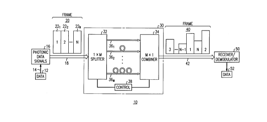
FIG. 1, as mentioned above, shows an optical time slot interchange
30 system 10 that does not have any eq~ ing of the photonic intensities. System 10
has a source of data 12, which is connected by link 14 to a source of photonic
signals 16. The data from source 12 may be any type of information, analog or
. CA 02138828 1998-04-22
- 3a-
digital. Link 14 may be electrical or optical depending on the needs of the system 10.
The source of photonic signals 16 could be any type of optical source, but a laser is
preferred. The data from source 12 modulates the photonic signals which are emitted
from source of photonic signals 16 along path 18. The type of modulation may be
5 any type, but those types with relatively constant intensities are preferred over the
types where the intensity amplitude variations bear the modulated data. An optical
data frame 20 is shown as it would appear along optical path 18. For standard
telephony purposes, optical data frame 20 would be 125 microseconds long, other
applications could have longer or shorter frames. Optical data frame 20 has multiple
10 time slots
2138~28
- 4 -
221 -22N for tr-A-n~...ill;.-g N individual m~ss~ges, or tr~n.~...;ll;.~g individual
portions of a time division multiplexed mess~A~ge using strict time division
mllltiplexing or the packet variation. All the slots 221 - 22N have the same in~cllsity
at this point.
S Path 18 is conn.octe~1 to an optical time slot inl~hallger (OTSI) 30.
There are numerous ways to make the OTSI 30, the emb~l;..-ent shown in FIG. 1 issimilar to that used by ThompsQn in Archileclure with Improved Signal-to-Noise
Ratio in Photonic Systems with Fiber-Loop Delay Lines, EEE Journal ON
SELECTED AREAS OF COMMUNICATIONS, August, 1988, page 1096. OTSI
10 30 has a lXM splitter 32 and a MXl combiner 34 connecte~l by delay paths
361 - 36 M . To 1- IA; 1~ i n frame int~ily, the nulll~ of delay paths, M, must be
equal to or greater than one less than twice the nu,l,be,l of slots, i.e., M22N- 1. A
controller 38, which in~ludes .n~ .. voltage driver circuits, controls the lXM
splitter 32 to switch the right slot to the right delay path for its desired time slot
15 inl~h~nge. Similarly, controller 38 also controls combiner 34 to switch the right
slot from the right delay path to be the output of the OTSI 30.
Optical data frame 40 shows how the ~ e ~il;es of the slots may be
~ffecte~l as time slots are int~ l-g~.d Frame 40 in FIG. 1 is a frame in~ y
m~int~ining e~ ple, but the invention is not limited to frame ~ in~ g
20 int~ -ges. In optical data frame 40, slot N has been delayed N-2 time slots and
inserted after slot 2 which was delayed only by the sllo, t~,;,l path from lXM splitter
32 to MXl combiner 34, hence, relatively no delay. Slot 1 has been delayed only
one time slot and inserted after slot N. Slot N-l has been dela~ed N time slots and
inserted after slot 1. The l~ nde~ of the slots N-2 to 3 are il~s~.t~l in desce-nding
25 order after slot N-l. The photonic il~len~ s of slots N and N-l are subst~nti~lly
less, bec~l.~ of the ~I(e .J~l;on of the long delay paths to which they were ~wilchcd,
than the photonic i'-t~n~;l;es of slots 2 and 1 because of the minim~l a'~ AIion of
their short delay paths. This re-ordered optical data frarne has dirr~.~,..tial
attenn~tion according to the amount of delay and any other &~ n~l;Qn cause in its
30 selecte~ path through the OTSI 30. The output of OTSI is lli~i-s...;l~ed alongpath 42
to receiver/de...~..l~tor 50.
Dirrel~ll ial alt~ v~l;on has a dev~ct~ting effect on the
receiver/~lemodul~tor 50. The receiver/~emod.ll~tQr 50 typically has an autom~tiC
gain control circuit which alt~ ls to adjust the gain to the average inlcn~ily level of
35 the received optical signal. When the average illt~ ily of the received signal is
high, the AGC circuit lowers its sensitivity. If, after lowering its sensitivity, the next
X~38828
- 5 -
time slot comes in with a lower power level, the l's in the signal are not strong
enough for the decision circuit in the receiver/dem~3~ tor 50 to decode as l's and
the entire time slot tends to be detectçd as all 0's. As the AGC circuit begins to
ramp up toward the end of this time slot, the data begins to be ~lu~ly decodable5 again. However, if the next time slot has a high photonic intensity level. This level
sAt,l.~te~ the receiver/dçmod~llAtor 50 because of the high value of the AGC circuit.
With the AGC circuit turned up, it begins to detect noise during the 0 bits as having
a high enough photonic h~t~ sily to be in~ ,ted as 1 's by the decision circuit of
the receiver/~çmod~llAtor 50. A dirÇe.~n~ial ~Att~nu~tion of only a few dB can
10 co-.-plet~ly dcstroy the bit elTor p~,rO ...~nce of the entirc OTSI system 10 and make
the demodulated data to data unit 52 useless.
~ efe~ing now to FIG. 2, an OTSI system 10A is shown accohling to
one embo.l;.--~,n~ of the present invendon. OTSI system 10A ove~olllcs the
dirr~lerllial ~tte~ Ation problem of OTSI system 10 that is shown in FIG. 1. System
15 10A has the same source of data 12, link 14, source of photonic signals 16 and path
18 as OTSI system 10. Thus, System 10A has the same type of data frame 20
applied to its input to OTSI 30A as system 10 applies to its input to OTSI 30. After
the input to OTSI 30A is where the ill.plo~c,llents of the present invention begins.
OTSI 30A has the ~l ~ . ,--AI ;on of each delay path 361 to 36M ~~ en
20 lXM splitter 32 and MXl cQI.lh;n ~ 34 ~ d~,t~ ,-,;.,~1, for example by llleaSUl~
at dme of rn~nnf~ct lre. The pre~ele. Il~n~fd ~t~nn~tion~ of the delay paths
361 -36M are stored in controller 38A. These ~ttenll~tionc are used with the data
frame re-ordenng data to dete ...ine the dme slot that is att~ t~l the most as it
propagates through OTSI 30A and then ~f te ~l~it~es~ either by c~l~ul~tion, or look-up
25 if the c~lcul~tion~ have been worked out ~rolehalld, the dirr.,l.,nce b.,l.b~ ~ n the
all~ n~l;on of the most ~ nual~ time slot and the l~es~ e alt..luation of each of
the other time slots. Thus, inside the controller 38A the amount of all~..u~lionl~fCC ~ to equalize t_e photoniG i.,t~,nsil~ of each data frame to the photonic
int~.,sil~/ of the most ~Ih-n~ eA time slot is available for each data frame as the data
30 frame leaves the output of OTSI 30A along path 42A. On path 42A, the dir~ences
in photonic h-le~-~il;es of the re-ordered time slots 40 are the same as those at the
output of OTSI 30 in FIG. 1.
A variable ~t~nu~tnr 60 is connected to the second end of path 42A to
receive the re-ordered data frame 40. Variable attenuator 60 is adjustable from a
35 l~in;rl~ amount, i.e..~.ini..~....~ insertion loss, to almost complete shut off, i.e. an
allel-uation of im'inite dB. The variable ~ttenll~tor 60 can be adjusted rapidly enough
2138828
-
-6-
to allow change for each individual time slot during the guard band portion of each
time slot. A cable 62Con~ variable atl~n~Atol 60 to the controller 38A. The
inrolmalion on the amount of allf ~ ;on needed for each time slot is carried from
controller 38A to variable attennAtor60 via cable 62. The receiver/dem~lllAtor 50
5 responds well to the equalized il,te~ y, even though the absolute intensity is lower.
Referring now to FIG. 3, one embo limf~nt of variable ~A~ Atol6ois
shown. A lX2 lithium niobate switch 70is the o~c.~ling element of the variable
~ttenllAtQr60. Switch 70 has control tf~minAl~ 72 and 73. T.ithinm niobate ~witches
are usually used as single pole double throw ~wilches that connecl the single pole
10 exclusively to one of two possible outputs according to two sets of drive voltages
across tf'rminAls 72,73. Byselectin~ voltages in ~l~neel1 the two drive voltages for
exclusive connection to an output, non-exclusive 'switch' connections are obtained.
In these non-exclusive connections~ a portion of the photonic intensity of each time
slot is con-e~/ed by the main optical path to the output of the variable ~ u~tor 70
15 and the remAinder is absc,ll~d or coll~e~ed to oblivion via a dead-ended optical
path 90 of the lX2 switch 70. The amount of the phol~n~;c int~nsily that is absorbed
or dead-ended is the amount of ?~ ;on, The amount of attenllfltion for each
drive voltage level is ~ ete ...;~ Pd at time of ...~-..r~ or at the time of
in~tAllAtiQn and used in the control circuits.
The lX2 switch 70 also has a digital to analog converter 76 that is
connecte~3 via cable 62 to controller 38A (shown in FIG. 2). Digital to analog
COll~,~,.t~,. iS also connecle~1 to a ~ l;- .. voltage driver 78. Controller 38A sends a
mes~ge to the digital to analog COIl~.t,. 76 with the ~ ;on l~qUil~d for the
current time slot. Digital to analog converter 76 converts this m~ ss~ge to an analog
voltage, which is ~mrlifie~l by driver 78 to drive lX2 switch 70 to the desired
~mollnt of ~n~ n for the current time slot. After being a~ d, the time slot
leaves the variable au~,n. at~, 70 as frame 82 of ullir~l~ intellsil.y and follows path
80 to recei~ lel..~l~ r 50. Those skilled in the art will recognize that the digital
to analog COll~,~,.t~ . 76 and the driver 78 could ~ltern~fiively be located in the
controller 38A, such a m~lificfltion is cleem~ to be within the scope of the present
invention.
Referring now to FIG. 4, a 2X2 lithium niobate switch 70B could be
used instead of the lX2 shown in FIG. 3. The dirr~ ce would be that the 2X2
lithium niobate switch 70B has a dead-ended input 92 as well as a dead-ended
35 output 90. Otherwise operation is esse~ti~lly the same. This embo~im~nt may be
more attractive if 2X2 lithium niobate switches have better cost or ~.Çollliance
2~3882~3
,
- 7 -
charaçteri~tics than lX2 because of wider use by industry.
Referring to FIGs. 2 and 3, in operation with the re-ordering of the slots
of OTSI 30A stored in the controller 38A, the AttenuAtion required to attenuate the
photonic intensity of each time slot to the intensity of the most alt~nualed time slot is
S de~c~ ned before that time slot reaches the variable att~nn~tor 60. During the guard
band be~ween time slots, the variable attenl1Ator 60 is set to provide the required
alh.'ualion to equalize the photonic intensity level of the current time slot with the
photonic inlellsily level that the controller 38A de~e ..-h~es will be the most
atl~..4Aled of all of the time slots of the data frame 40. Thus, all the time slots of the
10 data frame 82 are equalized to s~lbstAntially the same levd before the data frame
reaches receiver ~ernodlllatQr 50, and the bit error rate of the d~- ..od ~l~ted data sent
to data unit 52 greatly improved. Yet, each data frame is equalized to its own most
~ttçn-uate~ photonic inlensily level, which means that each time slot is only
~Ien~J~I~ as much as n~ess~ to equalize it with the photonic h,L~ ns;l;es of other
15 time slots in its l~ e data frame and no fixed a~ --u~l;ons which neerll~ssly
waste signal-to-noise ratios of the time slots are used in the present invention. For
eY~mple, if a data frame had no re-ordering as it passed through the OTSI 30A, all
time slots would be sent by the same minimal path, al~e-~.~a~ the minim~l amountby the OTSI 30A and the variable ~ttenu~tQr 60. In COII~aS ~ a system such as Koai's
20 would necess-~ ;ly have a preset attçn~ on to either the worst case or to some
cc,~ n~ ise case.
Thus, it will now be und.,l~lood that there has been ~ ç~sed a new
optical time slot int~l.;h~nger system, which uses a variable al~e .~to, to equalize
the photonic inhn~il;es of the re-ordered time slots of data within a data frame.
25 While the invention has been particularly illllsl~;~lrA and desçrihed with reference to
~efellrd c~bo li...ent~ thereof, it will be understood by those skilled in the art that
various ch~nges in form, details, and appliratiQn~ may be made therein. For
eY~mple, one or more optical amplifiers may be added into the opdcal paths to
increase the opdcal inlellsil~ of each time slot before or after the variable ~ttenllatnr
30 O~lah s to equalize the photoni~ inhsn~;l;es of the slots. It is acco.dillgly intended
that the appended claims shall cover all such ch~nges in form, details and
appliç~hons which do not depart from the t~ue spirit and scope of the invendon.