Note: Descriptions are shown in the official language in which they were submitted.
21 3~005
The present invention relates to a feedforward amplifier and,
particularly, to a feedforward amplifier for detecting distortion of an input signal
amplified by a feedforward loop and for amplifying the input signal while reducing
the distortion.
When an input signal including a plurality of frequency-multiplexed
carriers is amplified by an amplifier, intermodulation distortion occurs and is
mixed in an output signal of the amplifier. A known feedforward amplifier
removes a component of such distortion by means of a feedforward loop.
Figure 8 shows an example of a conventional feedforward amplifier.
In Figure 8, the feedforward amplifier is constructed such that it amplifies an input
signal having frequency in a high frequency band received at an input terminal
1 thereof and detects distortion introduced therein during amplification by means
of a distortion detecting loop 2. The distortion is removed by a distortion
removing loop 4 after the signal is passed through a power combiner circuit 3.
The output signal at terminal 6 is amplified with the distortion removed therefrom.
The distortion detecting loop 2 distributes the input signal through a
power distributor 11 to a main signal path 16 comprised of a first variable
attenuator 12, a first variable phase shifter 13 and a main amplifier 14, and a
linear signal path 17 including a first delay line 15. The power combiner 3
outputs a composite signal (difference signal) of the signals from the main signal
path 16 and the linear signal path 17. Combiner 3 outputs a main amplified
signal from the main signal path 16.
The distortion removing loop 4 includes a main amplifier output signal
path 22 including a second delay line 21 and a distortion signal injecting path 23.
A second variable attenuator 24, a second variable phase shifter 25 and an
auxiliary amplifier 26 are arranged in the distortion signal injecting path 23.
Signals passed through the main amplifier output signal path 22 and the distortion
signal injecting path 23 are combined by a power combiner 28. The power
distributor 11 and the power combiners 3 and 28 are of simple construction and
include, for example, transformer circuits, hybrid circuits and directional couplers,
etc.
21 39005
The operation of this conventional feedforward amplifier will now be
described. The high frequency band input signal applied to input terminal 1 is
branched into 2 channels 16, 17 by the power distributor 11. The high frequency
band input signal in one of the channels is amplified through the main signal path
16 including the first variable attenuator 12, the first variable phase shifter 13 and
the main amplifier 14. The input signal in the other channel is delayed by the
first delay line 15 of the linear signal path 17. The output signals of the mainsignal path 16 and the linear signal path 17 are supplied to the power combiner
3. The first delay line 15 of the linear signal line 17 and the first variable
attenuator 12, the first variable phase shifter 13 and the main amplifier 14 of the
main signal path 16 are regulated such that the two signals meet at the input
terminals of the power combiner 3. The two signals have the same amplitude
while the delay places the two signals in opposite phase. The output of the
power combiner 3 is therefore a difference signal therebetween.
The linear signal path 17 includes only the first delay line 15 and
therefore no distortion is produced. Consequently, any distortion introduced into
the input signal is generated or amplified by the first variable attenuator 12, the
first variable phase shifter 13 and the main amplifier 14 of the main amplifyingsignal path 16. The output of main amplifier 14 can be obtained as the difference
error, if the operation of the distortion detecting loop 2 is appropriate. This
distortion, that is, the difference signal, is output from a second output terminal
of the power combiner 3 to the distortion signal injecting path 23 and the output
signal of the main amplifier 14, which is the amplified input signal containing the
distortion, is directly supplied from a first output terminal of the power combiner
3 to the main amplifier output signal path 22.
Transfer functions of the two paths 22 and 23 extending from the input
terminals of the power combiner 3 on the side of the path 16 to the output
terminal of the power combiner 28 are regulated such that they have the same
amplitude and delay and opposite phase. Therefore, in the power combiner 28,
the distortion passed through the distortion signal injecting path 23 is added in
opposite phase to the amplified signal passed through the main amplifier output
r
21 39~05
signal path 22. Thus, the distortion of the amplified signal at the output terminal
6 of the power combiner 28 is cancelled out.
However, in the conventional feedforward amplifier mentioned above,
it is very diffficult to maintain a stable balance between the two feedforward loops
2 and 4 over a period of time since characteristics of the amplifier are affected
by variations in environmental temperature, etc.
For example, Laid-open Japanese Patent Application No. H1-198809
(published August 10, 1989) discloses a feedforward amplifier which is provided
with means for injeding a pilot signal of a specific frequency into a distortiondetecting loop for the purpose of enabling the feedforward amplifier to operate
stably. Figure 9 shows an example of such a conventional feedforward amplifier.
In Figure 9 components the same as those shown in Figure 8 are
assigned the same reference numerals and detailed description thereof is
omitted. An input signal applied to an input terminal 1 is supplied to a distortion
detecting loop 7 through a first directional coupler 40. The signal is amplified and
its distortion component is detected by the distortion detecting loop 7. The signal
is then supplied to a distortion removing loop 4 through a power combiner 3.
The distortion detecting loop 7 includes a main amplifiersignal path 16
including a power distributor 11, a second directional coupler 41, a first variable
attenuator 12, a first variable phase shifter 13 and a main amplifier 14, and a
linear signal path 17. The distortion removing loop 4 includes a linear signal path
22 and a distortion signal injecting path 23 including a second variable attenuator
24, a second variable phase shifter 25, an auxiliary amplifier 26 and a third
directional coupler 27. An output terminal of a power combiner 28 is connected
to an output terminal 6 through a fourth directional coupler 5. An oscillator 51outputs a pilot signal having a specific frequency which is input to the first
directional coupler 40 or the second directional coupler 41 through a switch 52
and to a mixer 33 of a sync detection circuit 32 including the mixer 33, a low-
pass filter 34 and a d.c. amplifier 35.
A high frequency switch 31 selects one output of the directional
couplers 5 and 27. The mixer 33 of the sync detection circuit 32 performs
frequency conversion of the constant frequency received from the oscillator 51
- 3 -
2 1 39005
with the output signal of the high frequency switch 31. A control circuit 53
controls the first variable attenuator 12 and the first variable phase shifter 13 or
the second variable attenuator 24 and the second variable phase shifter 25 on
the basis of the output of the sync detection circuit 32.
In this feedforward amplifier, when the distortion detecting loop 7 is to
be controlled, the switches 52 and 31 are switched to positions opposite to those
shown in Figure 9 so that the pilot signal is input to the first directional coupler
40 via the switch 52 and the signal from the auxiliary amplifier 26 is connectedto the sync detection circuit 32 through the third directional coupler 27. Thus, the
control circuit 53 controls the attenuation of the first variable attenuator 12 and
the phase shift of the first variable phase shifter 13 such that the level of the pilot
signal in the output signal of the auxiliary amplifier 26 becomes minimum. Thus,it is possible to minimize the distortion component that arises due to unbalanced
operation of the distortion detecting loop 7.
On the other hand, when the switches 52 and 31 are positioned as
shown in Figure 9, the pilot signal from the oscillator 51 is input to the main
amplifier signal path 16, and a signal branched by the directional coupler 5 from
the output signal of the power combiner 28 is input to the sync detection circuit
32 through the switch 31. In this case the control circuit 53 controls the second
variable attenuator 24 and the second variable phase shifter 25 such that the
level of the pilot signal contained in the output signal of the power combiner 28
becomes minimum. As a result, automatic regulation of the distortion removing
loop 4 becomes possible.
By executing the above mentioned controls of the distortion detecting
loop 7 and the distortion removing loop 4 continuously or intermittently, an
optimum operating condition of the feedforward amplifier is realized. Since the
signal applied to the input terminal of the feedforward amplifier is modulated for
information transmission and may be discontinuous in some cases, the operation
may become unstable if this input signal is used for the control signal. However,
since the feedforward amplifier performs control using the pilot signal whose level
and frequency are constant, stable control is possible.
- 4 -
2 1 39005
Nevertheless, the feedforward amplifier using the pilot signal has a
problem that, when the frequency of the pilot signal is set within an operating
frequency band, the control becomes unstable if there is an input signal having
a frequency which is identical to that of the pilot signal.
On the other hand, when the frequency of the pilot signal is set outside
of the operating frequency range, the characteristics of the constitutional
components of the paths 16 and 17 of the distortion detecting loop 7 or the paths
22 and 23 of the distortion removing loop 4 must be coincident in a wide
frequency range including the pilot signal frequency. For example, in order to
obtain a compression amount of 30 dB or more in the frequency range,
deviations of amplitude and phase must be within + 0.3 dB and + 2~,
respectively. These values correspond to a deviation between the pilot signal
frequency and the operating frequency when the pilot signal is completely
cancelled out. Therefore, it is desirable to set the pilot signal frequency as close
to the operating frequency as possible.
Further, the characteristics of the constitutional components of the
respective loops 7 and 4, such as the main amplifier 14 and the auxiliary amplifier
26, etc., vary with variations of ambient temperature, etc. In order to follow such
variations, it is necessary to control the distortion detecting loop 7 and the
distortion removing loop 4 as frequently as possible. However, when control of
the distortion detecting loop 7 is performed, the pilot signal may leak externally,
although the amount of leakage may be small.
Further, when the pilot signal is to be cancelled by, for example, 40 dB,
isolation required in the high frequency switches 52 and 31 must be 40 dB or
more. Unfortunately, a semiconductor switch capable of realizing an isolation aslarge as 40 dB (which is frequently used in a feedforward amplifier operating
around 1 GHz) is still not practical. Therefore, mechanical high frequency
switches having a life span which is generally shorter than that of semiconductor
switches must be used for the switches 52 and 31.
An object of the present invention is to provide a feedforward amplifier
capable of solving the above mentioned problems by setting a pilot signal
frequency at a predetermined value around an average frequency of an input
2 1 39005
signal and by continuously executing control of a distortion removing loop to end
the operation of a distortion detecting loop and the distortion removing loop.
In order to achieve the above object, a feedforward amplifier including
a distortion detecting loop for amplifying an input signal and for detecting
5 distortion generated by the amplification of the input signal, a power combiner for
deriving the distortion contained in the input signal amplified by the distortion
detecting loop and a distortion removing loop for cancelling out the distortion of
the derived distortion, comprises a variable frequency oscillator for outputting a
pilot signal having frequency controlled externally, a receiver for receiving the
10 distortion derived from a portion of the distortion removing loop and the amplified
signal whose distortion is cancelled out by the distortion removing loop, a first
control circuit for setting the frequency of the pilot signal from the variable
frequency oscillator to a value other than the frequencies of the input signal and
the distortion and close to an average value of the frequency of the input signal,
15 a second control circuit for controlling a transfer function of the distortion
detecting loop on the basis of a receiving level of the distortion component when
the pilot signal is input to the distortion detecting loop together with the input
signal, and a third control circuit for controlling a transfer function of the distortion
removing loop on the basis of a receiving level of an amplified signal whose
20 distortion is cancelled out when the pilot signal is supplied to a signal path of an
amplifying element in the distortion detecting loop.
In the invention as described above, the first control circuit sets the
frequency of the pilot signal of the variable frequency oscillator to a value other
than the frequencies of the input signal and the distortion and close to an
25 average value of the frequency of the input signal. Therefore, the frequency of
the input signal to the distortion detecting loop, which is to be amplified thereby,
is never identical to that of the pilot signal and the pilot signal frequency can be
set as close as possible to the input signal frequency to be amplified.
Further, according to the present invention, a fourth control circuit
30 controls the distortion detecting and removing loops such that the control of the
distortion removing loop is performed normally by the third control circuit and the
control of the distortion detecting loop is performed by the second control circuit
- 6 -
21 39005
when an environmental condition is changed largely. Therefore, the control time
of the distortion detecting loop can be minimized.
Embodiments of the invention will now be described, by way of
example, with reference to the accompanying drawings, wherein:
Figure 1 shows a block diagram of an embodiment of a feedforward
amplifier according to the present invention;
Figure 2 is a flowchart of an operation of the embodiment shown in
Figure 1;
Figure 3 is a flowchart of a first step of the operation shown in Figure
2;
Figure 4 is a flowchart of a second step of the operation shown in
Figure 2;
Figure 5 is a flowchart of a third step of the operation shown in Figure
Figure 6 is a flowchart of a fourth step of the operation shown in Figure
2;
Figure 7 is a flowchart of a re-control operation of a distortion detecting
loop of the embodiment shown in Figure 1;
Figure 8 is a block diagram of an example of a conventional
feedforward amplifier; and
Figure 9 is a block diagram of another example of a conventional
feedforward amplifier.
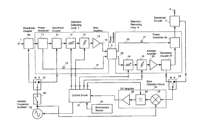
Figure 1 shows an embodiment of a feedforward amplifier according
to the present invention. In Figure 1, components which are the same as those
shown in Figure 9 are depicted by the same reference numerals, and detailed
explanation thereof is omitted.
In Figure 1, a control circuit 61 controls the attenuation of a first
variable attenuator 12 and the phase shift of a first variable phase shifter 13 of
a distortion detecting loop 7, the attenuation of a second variable attenuator 24
and the phase shift of a second variable phase shifter 25, the cut-off frequencyof a variable low-pass filter 65 of a sync detection circuit 54 and the oscillation
frequency of a variable frequency oscillator 62. The variable frequency oscillator
~'~ '~
. .
~ 7 --
2 1 390U5
62 is a voltage-controlled oscillator whose output frequency is variably controlled
by an output voltage of the control circuit 61 and is used as a pilot signal.
A high frequency switch 63 is an on/off switch controlled by the control
circuit 61 and connects the output signal (the pilot signal) of the variable
5 frequency oscillator 62 to a high frequency switch 52, or disconnects the output
signal of the oscillator 62 from the high frequency switch 52. An environment
sensor 64 detects environmental conditions such as ambient temperature and
outputs an electric signal having a level corresponding to the detected conditions.
The high frequency switch 53 selects one of the output signals of the directional
couplers 5 and 27 and supplies it to the mixer 33 of the sync detection circuit 54.
The high frequency switches 52 and 53 are controlled by a switching signal from
the control circuit 61 similar to the control of the high frequency switch 63.
Operation of this embodiment will now be described. In the
feedforward amplifier of this embodiment, an operation involving four steps is
15 performed in the sequence shown in Figure 2 under the control of the control
circuit 61. That is, in the first step, the frequency of the pilot signal is determined
(step 100), in the second step, the distortion detecting loop 7 is controlled (step
200), in the third step, the distortion removing loop 4 is controlled (step 300) and,
finally, in the fourth step, the normal state control is performed (step 400). The
20 operation of the respective steps will now be described in detail.
(1) First Step (100)
The determination of the pilot signal frequency in the first step 100 is
performed according to the flowchart shown in Figure 3. First, the switch 53
shown in Figure 1 is connected to terminal A such that the output signal of the
25 feedforward amplifier is input through the fourth directional coupler 5 and the
switch 53 to the sync detection circuit 54 (step 101). The high frequency switch63 is turned OFF (step 102) such that the pilot signal is not input to the distortion
detecting loop 7. Thus, only the input signal received from the input terminal 1is allowed to pass to the power distributor 11 via the first directional coupler 40
30 in which it is divided into two signals. One of these signals is input to the main
amplifier 14 via the second directional coupler 41, the first variable attenuator 12
and the first variable phase shifter 13, and the other signal is input to the power
2 1 39005
combiner 3 after being delayed by the first delay line 15. The input signal is, for
example, a signal obtained by time-division of five multiplexed carriers having
identical amplitude and the feedforward amplifier linearly amplifies these five
carriers simultaneously.
As described previously, the power combiner 3 not only outputs the
output signal of the main amplifier 14 directly from the first output terminal to the
main amplifier signal path 22 of the distortion removing loop 4, but also combines
the output of the main amplifier 14 with the input signal from the delay line 15,
derives distortion generated by the constitutional components of the path 16, and
outputs, from the second output terminal, the distortion to the distortion signal
injecting path 23 of the distortion removing loop 4. The distortion removing loop
4 cancels out the distortion input to the distortion signal injecting path 23 in a
manner similar to that in a conventional feedforward amplifier, and outputs the
amplified and distortion removed signal from the power combiner 28 through the
fourth directional coupler 5 to the output terminal 6 and the switch 53, as the
output signal of the feedforward amplifier.
In this case, the control circuit 61 controls the output oscillation
frequency (pilot signal frequency) of the variable frequency oscillator 62 to a
certain frequency so that the sync detection circuit 54 performs sync detection at
that frequency (step 103). The control circuit 61 stores the frequency and levelof the output signal of the feedforward amplifier which were synchronously
detected by the sync detection circuit 54 (step 104). Then, the control circuit 61
changes the output oscillation frequency of the variable frequency oscillator 62to another frequency such that the sync detection circuit 54 operates at the newfrequency (step 105) and then determines whether or not the new frequency is
within the predetermined available frequency range (step 106). If it is within the
predetermined available frequency range, the control circuit 61 re-stores the
frequency and level of the output signal of the feedforward amplifier which weresynchronously detected in step 104.
In this manner, the control circuit 61 stores the frequency and level of
the output signal of the feedforward amplifier while sequentially changing the sync
detection frequency of the sync detection circuit 54 within the available frequency
B g
21 ~9005
range by controlling the output frequency of the variable frequency oscillator 62
(steps 109 to 1 11).
Thus, the frequency of the intermodulation distortion between the five
carriers, generated by amplifying the input signal by the main amplifier 14, is
detected. In a case where the control circuit 61 is capable of computing a
frequency component of the distortion associated with a frequency and level of
the input signal, there is no need to perform the processing in steps 109 to 111.
Thereafter, the control circuit 61 calculates an average value of the
frequencies (in this embodiment, 5 carrier frequencies) of the input signal stored
in step 104 (step 1 12) and then the pilot signal frequency is determined in steps
113 and 114. However, it is impossible to perform stable high speed control if
the pilot signal frequency is coincident with the frequency of the input signal or
with the distortion frequency generated due to the presence of the input signal.Furthermore, highly precise frequency characteristics of the two loops 7 and 4 are
required if the pilot signal frequency differs considerably from the input signal
frequency.
In view of this fact, in this embodiment, the pilot signal frequency is set
to a value which is neither the input signal frequency stored in step 104 nor the
distortion frequency generated by the input signal stored in step 109, but is set
around the average value of the input signal frequencies calculated in step 112
(steps 113 and 114).
Alternatively, in a case where the number of carriers of the input signal
is few and the carrier frequencies of the input signal are predictable, it may be
possible to select a suitable frequency without scanning the sync detection
frequency in the sync detection circuit 54, and then to confirm that it is coincident
with neither the input signal frequency nor the distortion frequency by switching
the switch 53 between the terminals A and B.
(2) Second Step (200)
Control of the distortion detecting loop 7 is performed according to the
30 flowchart shown in Figure 4. First, the high frequency switch 63 shown in Figure
1 is turned ON (step 201) and then the high frequency switches 52 and 53 are
connected to the terminals B (steps 202 and 203). With this procedure, the pilot
- 10-
21 39005
signal generated by the variable frequency oscillator 62 (having a frequency
determined in the First Step) is supplied through the high frequency switch 63,
the switch 52 and the first directional coupler 40 to the distortion detecting loop
7. The output distortion component of the auxiliary amplifier 26 is supplied
5 through the third directional coupler 27 and the switch 53 to the sync detection
circuit 54. In this case, it is possible for the control circuit 61 to improve the
signal to noise ratio (S/N ratio) of the sync detection circuit 54 by controlling the
cut-off frequency of the variable low-pass filter 65 contained in the sync detection
circuit 54, such that the pass band of the sync detection circuit 54 is narrowed.
10Then, the control circuit 61 applies suitable control voltages to the
variable attenuator 12 and the variable phase shifter 13 (step 204). After the
detection level of the sync detection circuit 54, that is, the level of the pilot signal,
at that time is measured (step 205), the control voltages are changed to other
values (step 206) and the detection level of the pilot signal of the sync detection
15circuit 54 is measured again (step 207).
The pilot signal level sync detected at that time by the sync detection
circuit 54 is the distortion level indicative of an error between signals in the paths
16 and 17 of the distortion detecting loop 7 which are equal in amplitude and
opposite in phase. Therefore, the control circuit 61 controls the variable
20 attenuator 12 and the variable phase shifter 13 with control voltages with which
a low detection level of the measured pilot signal is obtained (step 208).
Then, the control circuit 61 decides whether or not the detection level
of the pilot signal at that time is lower than a predetermined value (step 209) and,
if it is higher, the process is returned to step 205. In this manner, the control
25 circuit 61 controls the amount of attenuation of the variable attenuator 12 and the
amount of phase shift of the variable phase shifter 13 such that the level of the
pilot signal detected by the sync detection circuit 54 and input to the control
circuit 61 becomes a minimum value which is smaller than the predetermined
value. The control method in this case is preferably based on an algorithm
30 having a high converging speed, such as the steepest descent method.
Thereafter, the control circuit 61 ensures that the pilot signal frequency
is coincident with neither the input signal frequency at the input terminal 1 nor the
- 11 -
2 1 39005
distortion frequency associated with this input signal by turning the high
frequency switch 63 OFF (step 210).
(3) Third Step (300)
Control of the distortion removing loop 4 is performed according to the
flowchart shown in Figure 5. First, the high frequency switch 63 shown in Figure1 is turned ON (step 301) and then the high frequency switches 52 and 53 are
connected to the terminals A (steps 302 and 303). With this procedure, the pilotsignal generated by the variable frequency oscillator 62 (having frequency
determined in the First Step) is supplied through the high frequency switch 63,
the switch 52 and the second directional coupler 41 to the path 16 of the
distortion detecting loop 7. The output signal of the distortion removing loop 4is supplied through the fourth directional coupler 5 and the switch 53 to the sync
detection circuit 54.
The control circuit 61 applies initial values of the control voltages to the
variable attenuator 24 and the variable phase shifter 25 (step 304). After the
detection level of the sync detection circuit 54, that is, the level of the pilot signal,
at that time is measured (step 305), the control voltages are changed to other
values (step 306) and the detection level of the pilot signal of the sync detection
circuit 54 is measured again (step 307).
The pilot signal level sync detected by the sync detection circuit 54 at
that time is the distortion level which is indicative of an error between signals in
the paths 22 and 23 of the distortion removing loop 4, which signals are equal in
amplitude and opposite in phase. Therefore, the control circuit 61 controls the
variable attenuator 24 and the variable phase shifter 25 with control voltages with
which a low detection level of the measured pilot signal is obtained (step 308).The control circuit 61 decides whether or not the detection level of the
pilot signal at that time is lower than a predetermined value (step 309) and, if it
is higher, the process is returned to step 305. In this manner, the control circuit
61 controls the amount of attenuation of the variable attenuator 24 and the
amount of phase shift of the variable phase shifter 25 such that the level of the
pilot signal detected by the sync detection circuit 54 and input to the control
- 12-
21 39005
circuit 61 becomes a minimum value which is smaller than the predetermined
value.
Thereafter, the control circuit 61 confirms that the pilot signal frequency
is coincident with neither the input signal frequency at the input terminal 1 nor the
5 distortion frequency associated with this input signal by turning the high
frequency switch 63 OFF (step 310). The control circuit 61 stores the control
voltages of the variable attenuator 24 and the variable phase shifter 25 and theoutput voltage of the environment sensor 64, at this time, into memory (step 311).
(4) Fourth Step (400)
Control in the normal state in the Fourth Step is performed according
to the flowchart shown in Figure 6. It should be noted that, at the end of the
control in the Third Step, the optimum operation of the feedforward amplifier isrealized. However, from time to time, the control must follow variations in gainand phase of the amplifier due to variations in environmental conditions, such as
15 ambient temperature.
Further, although the attenuation of the distortion removing loop 4
directly determines the attenuation of distortion, the attenuation of the input signal
by the distortion detecting loop 7 is to prevent the level of the input signal leaked
to the auxiliary amplifier 26 from becoming too high. Therefore, when there is
20 some margin in the output of the auxiliary amplifier 26, the amount of attenuation
of the distortion removing loop 4 becomes correspondingly flexible. Further,
when the distortion detecting loop 7 is controlled, the pilot signal leaks externally.
According to this embodiment, control of the distortion removing loop
4 is performed in the normal state, as the Fourth Step of control. Usually, there
25 is almost no case where the control voltages are largely changed in the normal
state, it is preferable to use a control method in which respective control voltages
are changed slightly. Therefore, in the Fourth Step, after the control circuit 61
controls the amount of attenuation of the variable attenuator 24 and the amount
of phase shift of the variable phase shifter 25, with the control voltages for the
30 lower detection level of the pilot signal detected by the sync detection circuit 54
and input to the control circuit 61 through steps 401 to 408 similar to the control
steps 301 to 308 of the distortion removing loop 4 in the Third Step, the control
13 -
21 39005
circuit 61 determines whether or not the control voltages largely deviate from the
predetermined values (step 409).
If there is no large deviation, the control circuit 61 determines whether
or not a constant time period has lapsed after the previous control of the
5 distortion detecting loop 7 (step 410). If the constant time is not lapsed, it is
confirmed by turning the high frequency switch 63 OFF whether or not the pilot
signal frequency is coincident with neither the input signal frequency nor the
distortion frequency associated with the input signal (step 411). Then, by
changing the control voltages, the process is returned to step 405 to obtain the10 control voltages with which a lower detection level of the pilot signal is obtained.
On the other hand, if it is decided in step 409 that the control voltages
have deviated largely, it is assumed that the large deviation of the control
voltages of the distortion removing loop 4 is due to a large environmental change
since the distortion detecting loop 7 and the distortion removing loop 4 are
15 assumed to be under substantially the same environmental conditions and the
distortion removing loop 4 is assumed to be always controlled at the optimum
value. Therefore, the control circuit 61 decides that it is necessary to control the
distortion detecting loop 7. After it controls the distortion detecting loop 7 again
(step 412), it returns to step 402 to control the distortion removing loop 4 in the
20 normal state.
Further, since the respective constitutional components of the
feedforward amplifier are subject to age variation, it is necessary to activate the
distortion detecting loop 7 with a relatively long time interval. Therefore, when
it is decided in step 410 that the constant time from the previous control of the
25 distortion detecting loop 7 has lapsed, the control circuit 61 decides also that
control of the distortion detecting loop 7 is necessary and, after it controls the
distortion detecting loop 7 again (step 412), it returns to step 402 to control the
distortion removing loop 4 in the normal state.
Re-control of the distortion detecting loop 7 in step 412 is performed
30 according to the flowchart shown in Figure 7. This re-control is similar to the
control of the distortion detecting loop 7 in the Second Step described with
respect to Figure 4. After the control circuit 61 connects the high frequency
-,~.s~ - 14-
~ ~:r
2l 3~005
switches 52 and 53 to the terminals B (steps 4121 and 4122), the control circuit61 controls the amount of attenuation of the variable attenuator 12 and the
amount of phase shift of the variable phase shifter 13 such that the level of the
pilot signal detected by the sync detection circuit 54 and input to the control
5 circuit 61 becomes a minimum value which is smaller than the predetermined
value (steps 4123 to 4128).
Thereafter, it is confirmed by turning the high frequency switch 63 OFF
that the pilot signal frequency is coincident with neither the input signal frequency
nor the distortion frequency associated with the input signal (step 4129). Then,10 at a time when the control of the distortion detecting loop 7 is completed, the
distortion removing control voltages for the variable attenuator 24 and the
variable phase shifter 25 and the output voltage of the environment sensor 64 are
updated and stored into the memory of the control circuit 61 (step 4130).
It is possible in step 409 shown in Figure 6 to compare the output
voltage of the environment sensor 64 stored in the Third Step (step 311) with the
current output voltage of the environment sensor 64 to decide whether or not thecurrent voltage has changed largely from the predetermined value and, if it has
changed largely, the distortion detecting loop 7 is controlled again.
According to this embodiment, a feedforward amplifier is provided
which can be stably controlled by performing four control steps sequentially,
which is comprised of components having frequency characteristics not as
precise as required in a conventional feedforward amplifier, and which is durable
for a long time due to the reduced number of controls of the distortion detecting
loop.
As described above, according to the present invention, the pilot signal
frequency is never coincident with the frequency of the signal input to the
distortion detecting loop and therefore it is possible to stably control the
feedforward amplifier. Further, since the pilot signal frequency can be set around
the frequency of the input signal to be amplified and the frequency characteristics
of one of the two paths in the distortion detecting loop are not required as
precisely coincident with those of the other, and that this is also true for thedistortion removing loop, the feedforward amplifier can be easily constructed.
, ~ - 15-
2 1 390~5
Since the control time of the distortion detecting loop can be made
short through the Fourth Step, the external leakage of the pilot signal is
minimized. Further, since the frequency of switching the control between the
distortion detecting loop and the distortion removing loop is lower than that in a
5 conventional feedforward amplifier, it is possible to construct a feedforward
amplifier having a longer life than a conventional amplifier, even if mechanicalhigh frequency switches are used.
- 16-