Note: Descriptions are shown in the official language in which they were submitted.
2139027
PHA 21.861 l 09.12.1994
Circuit arr~ngernçnt
The present invention relates to a circuit arrangement for operating a
larnp.
High &equency converters are known and have many useful applications
in electronic technology. One particularly attractive application thereof is for the supply
5 of regulated electric energy to electric discharge lamps. One of the desirable features of
a high frequency converter is that it has a high power factor as seen from the 60 Hz (50
Hz) AC power lines.
One example of a conventional high-frequency AC/AC converter system
with a corrected input power factor is shown in Fig. 1, where a boost converter is
10 provided for power factor correction and a push-pull inverter is used for high-frequency
DC/AC power conversion. An electro-magnetic interference filter (EMI filter) is
coupled to a pair of input terminals which supply, for example, a 60 Hz sinusoidal AC
line frequency of a nominal voltage of 115 volts. The EMI filter is used to filter out the
high frequency noise generated by the high frequency operation of the boost converter
15 and the push-pull inverter. The AC line voltage is rectified by a full bridge diode
rectifier circuit.
In Fig. 1, a boost converter 1 which provides power factor correction is
coupled to the output terminals of the bridge rectifier circuit. The boost converter in its
elemental form consists of an inductor L and a diode D connected in series circuit
20 b~ween a first input terminal and a first output terminal of the boost converter. The
second input terminal and the second output terminal of the boost converter are
conn~ted in common. An energy storage capacitor Ce is connected across the first and
second output terminals of the boost converter. A switching field effect transistor Q is
conn~ted to a junction point between the inductor L and the diode D and to the
25 common line connecting the second input and output terminals. The body diode and
inherent capacitance Cds of the MOSFET Q is shown in parallel therewith. The gate
electrode of the MOSFET Q is coupled to the output of a control circuit A.
In the boost converter stage, the current flowing through the inductor L is
2139027
._
PHA 21.861 2 09.12.1994
monitored and is compared in the control circuit A with reference values generated
from the rectified voltage. The current waveform is shaped to have the same waveform
as and to be in phase with the rectified voltage waveform by controlling the ON duty
ratio and/or the switching frequency of the MOSFET switch Q. The output of the boost
5 converter is a DC voltage roughly regulated by the control circuit A. This DC voltage
is then inverted into a high frequency AC voltage by the high frequency push-pull
DC/AC inverter 2.
The high frequency DC/AC inverter has its input terminals conne~ted
directly to the output terminals of the power factor correction boost converter 1. A first
10 input terminal of the high frequency inverter is connected to a common junction point of
a pair of primary windings Npl and Np2 of an output transformer T. A secondary
winding N of the transformer is coupled to a series circuit consisting of an inductor Lr
and a capacitor Cr. The load is connected across the terminals of the capacitor Cr. One
end of the primary winding Npl and one end of the other primary winding Np2 are
15 conn~ted to the common output line via the MOSFET transistor switches Ql and Q2,
fespeclively. The respective body diodes and inherent capacitances of the MOSFETtransistors Ql and Q2 are also shown in the drawing. The gate electrodes of the
MOSFET switching transistors Ql and Q2 are connected to respecli~e outputs of a
control circuit B.
The high frequency power developed in the high frequency push-pull
DC/AC inverter 2 is delivered to the load via the transformer T. The control circuit B
has an input coupled to the load and is used to feed back the output power so as to
control the operation frequency of the MOSFET switches in the high frequency DC/AC
inverter so that a regulated output power can be obtained. Since the input power of the
system has a low frequency (100 Hz or 120 Hz) component and the output power of the
system is a regulated high frequency power, the storage capacitor Cc is requiredbetween the boost converter and the push-pull inverter for energy storage in order to
balance the input power and the output power.
An important disadvantage of the conventional high frequency converter
30 circuit shown in Figure 1 is that the voltage stress on the MOSFET switches Ql and Q2
in the push-pull inverter 2 is high. If the ON duty ratio of the MOSFET switch Q in the
boost converter is 50 percent, the voltage across the energy storage capacitor Ce will be
twice the amplitude of the AC line voltage. In this case, the voltage stress on the
2139027
PHA 21.861 3 09.12.1994
MOSFET switches in the push-pull inverter will be four times the amplitllde of the line
voltage. The voltage stress can be reduced by employing a smaller duty ratio. However,
the voltage across the energy storage capacitor will always be higher than the amplitude
of the line voltage due to the boost converter operation. Typically, it is de~igned to be
5 1.5 times the amplitude of the line voltage. In that case, the voltage stress on the
MOSFET switches Q1 and Q2 in the push-pull inverter will still be three times the
amplitude of the line voltage.
It is also known to use a half-bridge inverter instead of the push-pull
inverter in order to reduce the voltage stress on the MOSFET switches in the inverter.
10 However, in this case, one of the two MOSFET switches is in the high voltage side of
the circuit. A high-side driver is then required to drive the high side MOSFET,
resulting in additional cost and complexity of the overall circuit.
In order to simplify the control circuit A, a discontinuous conduction
mode (DCM mode) is usually adopted for the boost converter for power factor
15 correction. In the DCM mode, the current flowing through the inductor L is
discontinuous. If the ON duty ratio of the MOSFET Q is fixed, the peaks of the current
through the inductor L will follow the waveform of the rectified line voltage. Therefore,
a high input power factor can be obtained after the high frequency components of the
inductor current are filtered out by the EMI filter. In this case, the fee~dbac-k of the
20 rectified voltage and the monitoring of the inductor current can be elimin~t~d.
The conventional high frequency converters disçl-csed above each include
two high frequency power stages and two co"es~,onding control circuits. One stage is
for the input power factor correction and the other stage is for the DC/AC powerconversion.
It is therefo~ an object of the present invention to provide a high
frequency push-pull AC/AC converter system with input power factor correction inwhich the voltage stress on the high frequency switching transistors is significantly
30 reduced over that of known conventional high frequency converters.
It is another object of the invention to provide a high frequency push-pull
AC/AC converter system with input power factor correction which requires fewer
semiconductor and other circuit components than in the prior art thereby re~ucing the
2139027
PHA 21.861 4 09.12.1994
size and complexity of the converter system which in turn provides a cost saving.
Another object of the invention is to provide a high frequency push-pull
AC/AC power factor co.lected converter system in which the boost converter stage and
the high frequency inverter stage are combined into a single stage thereby saving one
5 power stage and one control circuit while preserving all of the required functions of the
conventional two-stage high-frequency converter system.
The foregoing objects and other advantages are provided in accordance
with the present invention wherein a transformer, an inductor, an energy storagec~citor, first and second high frequency switching transistors and a single control
10 circuit are coupled together in a novel and unique circuit arrangement that provides the
power factor correction of the boost converter and the high frequency inverter function
of the prior art systems, all in a single stage of the new circuit.
As a result of the invention, one MOSFET device is saved and hence one
control circuit is also elimin~çd, which achieves a significant cost reduction. The
15 voltage stress on the switching transistors is reduced to half that of the conventional
ACtAC convener system using a push-pull invener. An easier and cheaper MOSFET
selection then is possible. Funhermore, both MOSFET switches are connected to
ground so that, compared with the half-bridge invener, a high side driver is eliminated.
It then becomes easier to integrate the power MOSFETs with the control circuit. All of
20 the MOSFET devices are zero-voltage-switched so that high frequency operation is
possible and with a low degree of noise generation. The frequency of the high
frequency current at the input of the rectifier is doubled due to the interleaving of the
two power factor correction circuits. The current ripple thus is reduced so that the
design of the EMI filter is simpler and easier. In one embodiment, the current in the
25 power factor correction inductor is distributed in two inductors.
The foregoing and other objects and advantages of the invention will be
better appl~iated from the following detailed description of the invention when taken in
30 conjunction with the accompanying drawings in which:
Fig. 1 is a block schematic diagram of a conventional AC/AC converter
system using a boost converner for power factor correction and a push-pull inverner for
DC/AC power conversion,
2139027
-
PHA 21.861 5 09.12.1994
Fig. 2 is a block schematic diagram of a first embodiment of the
invention;
Fig. 3 is a block diagram of ~the control circuit used in the converter of
Fig. 2,
Figs. 4A - 4G show waveforrn diagrams helpful in describing the
operation of the control circuit of Fig. 3,
Fig. 5 is a diagrarn showing the operating characteristic of the voltage
controlled oscillator of the control circuit,
Fig. 6 is a block schematic diagram of a second embodiment of the
10 invention, and
Fig. 7 is a block schematic diagram of a third embodiment of the
invention.
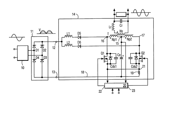
Fig. 2 shows a high frequency push-pull AC/AC converter apparatus with
input power factor correction in accordance with the invention. An electro-magnetic
interference (EMI) filter 10 has its input coupled to terminals for supplying a 60 Hz (50
Hz) AC voltage from the usual available AC power line. The output of the EMI filter is
coupled to input terminals of a full wave diode rectifier bridge circuit 11 having first
20 and second output terrninals coupled to first and second input terminals 12 and 13,
r~s~lively, of the high frequency push-pull converter circuit 14.
The input terminal 12 is connected to an inductor Ll and to an inductor
L2. The inductors Ll and L2 in turn are connected to diodes D5 and D6, respectively.
The diode D5 is connected to one end 16 of a primary winding Npl of an output
25 transformer T and diode D6 is connected to one end 17 of the primary winding Np2 of
the output transformer. The common junction point 15 of the windings Npl and Np2 is
conn~cted via an energy storage capacitor Ce to a common line 18 connected to the
teln~inal 13.
The end point 16 is conn~cted via a MOSFET switching transistor Ql to a
30 current sensor resistor 19 which in turn is connected to the common line 18. The other
end point 17 is conne~ted via a second MOSFET switching transistor Q2 to the current
sensor resistor. The terminal 15 is coupled to an input of a control circuit 20 to supply
a control signal thereto that is determined by the voltage Vc stored on the capacitor Ce.
2~39027
PHA 21.861 6 09.12.1994
The tcllllinal 21 of the resistor 19 is coLFled to another control input of the control
circuit 20 to supply a control signal thereto that is determined by the currents IQl, IQ2
that flow in the switching transistors Ql and Q2, res~;li~ely. The control circuit in
turn has output terminals 22 and 23 that supply switch control signals to the gate
S electrodes of high frequency switching transistors Ql and Q2, r~s~ ely.
The secondary winding Ns of the output tran~rGI~er T is connect~d to a
series circuit conlposed of an inductor Lr and a capacitor Cr. A load is c~nn~cted across
the terminals of the c~pacitor Cr which constitute the output terminals of the high
frequency push-pull converter. The winding sense of the transformer windings is
10 indicated by the conventional dot symbols.
The high frequency push-pull converter circuit of Fig. 2 operates as
follows: The two MOSFET switches Ql and Q2 are turned on and off in a
complementary manner, preferably with a 50 percent duty ratio as in the case of a
conventional push-pull inverter. The inductor Ll, diode D5 and MOSFET Ql form a
15 boost converter for power factor correction. The inductor L2, diode D6 and MOSFET
Q2 form another boost converter. The inductance values of inductors Ll and L2 are
designed to be equal. If the duty ratio is fixed, the boost converter will be opel~dted in
the discontinuous conduction mode so that it can be controlled by frequency rnodulqtion.
When one of the MOSFETs, e.g. Ql, is turned on, the rectified line
20 voltage is applied to the inductor Ll. Its current rises linearly from zero as follows:
~ i"
Ll (1)
where, I Vjn I in-licates the magnitude of the rectified line voltage during the ON
25 period of tr~n~istQr Ql, which can be considered to be constant over a high frequency
switching cycle. The electric energy is stored in the inductor Ll during the ON period
of transistor Ql. The peak current is obtained as follows:
i~p = Li~- x 0.5T5
(2)
2139027
PHA 21.861 7 09.12.1994
where, Ts is the switching cycle.
When MOSFET Q1 is turned off by the control circuit 20, the MOSFET
Q2 is turned on. There is a short dead-time at the switch over when transistors Q1 and
Q2 are both simultaneously off. The voltage Vc across the energy storage c~pa~itor Ce
S is applied to the transfollller primary winding Np2, inducing a voltage in winding Npl.
As a result, an equivalent voltage source 2Vc is conn~t~ to the inductor L1. Theinductor current charges the capacitor Ce through winding Npl. Energy is transferred
from inductor L1 to car~cit~r Ce. during the off period of the MOSFET Q1, current
through the inductor L1 falls linearly from a peak value to æro:
iL = -- 0.S x T -- ~
Ll ' L, (3)
When the current falls to æro, it is clamped to zero thereafter by the
diode D5. If the converter is so designed that the inductor current iL falls to zero just
15 prior to the turn-on of MOSFET Q1 during the line peak period, then:
V~ = (Vh)~,....
(4)
from equation (3). Here, (Vin)a,np in-licates the amplitude of the line voltage. Thefefol~,
20 the voltage stress on the MOSFET Ql is twice the amplitude of the line voltage.
Compared with the conventional push-pull AC/AC converter system, the voltage stress
is reduced.
As can be seen from equation (2), the peak of the inductor current is
pfo~ollional to the input voltage if the switching frequency is fixed. The peaks of the
25 current through inductQr L1 follow the waveform of the rectified line voltage. The other
half of the boost converter consisting of inductor L2, diode D6 and MOSFET Q2
operates exactly the same as the one consisting of L1, D5 and Ql, but with the half
switching cycle shifted. The two boost converters act as interleaved power factor
correction converters. The peaks of the sum of the two inductor currents, i.e. the
30 current flowing through the rectifier circuit, also closely follow the waveform of the
rectified line voltage. Therefore, a high input power factor can be obtained after the
high frequency current components are filtered by the EMI filter. The high frequency
ripple of the current flowing through the rectifier 11 is reduced and the ripple frequency
2139027
PHA 21.861 8 09.12.1994
is doubled by the in~erl~ving of the two boost converters as cG"")ared with a
conventional AC/AC converter system. The peak inductor current is also reduced to
half. As a result, the design of the EMI filter is easier. The input power is controlled by
frequency modulation of the switching transistors Q1 and Q2.
The MOSFETs Q1, Q2, transformer T, resonant inductor Lr, resonant
capacitor Cr, and the load together form a high frequency push-pull DC/AC inverter.
Its principle of operation is the same as that of the conventional high frequency push-
pull DC/AC inverter. The DC voltage Vc developed across the energy storage c~p~citQr
Ce is inverted into a squarewave voltage at the secondary winding Ns of the output
10 transformer by the on-off operation of the switching transistors Q1 and Q2. The
squarewave voltage is filtered to produce a sinusoidal voltage by means of the L-C
resonance of inductor Lr and capacitor Cr. The sinusoidal voltage across the resonant
capacitor Cr is applied to the load. The voltage across the secondary winding Ns is a
squarewave, the current flowing through the resonant inductor Lr is sinusoidal as is the
15 output voltage across the resonant capacitor Cr when the load is a pure resistive load.
If the switching frequency is chosen to have a value above the resonant
frequency, zero-voltage-switching can be realized for the two switching transistors Ql
and Q2 if a small dead time is provided in the gate control signals. During the dead
time, both MOSFETs are off simultaneously. The current through the resonant inductor
20 will charge one drain-source capacitor, for example, Cdsl and discharge the other
drain-source capacitor Cds2. Therefore, the drain-source voltage rises up gradually after
the MOSFET is turned off and falls to zero before the other MOSFET is turned on.Thus, zero voltage switching is achieved. Each MOSFET, Ql and Q2, serves both for
power factor correction and for high frequency power conversion.
Figure 3 is a block diagram of one possible form of the control circuit 20
of Fig. 2. The voltage on the storage capacitor Ce at termina1 15 of Fig. 2 is coupled to
the input terminals 24 and 25 of the control circuit of Fig. 3. A voltage propollional to
the currents flowing through the switching transistors Ql and Q2, IQl and IQ2,
developed at terminal 21 in Fig. 2 is coupled to the input terminal 26 of the control
30 circuit. In addition, a fee~b~ck voltage (VOUt) developed across the output (load) is
coupled to input terminals 27 and 28.
The input terminals 27 and 28 are coupled to the primary winding of a
transformer 29 having a secondary winding coupled to input terminals of a diode
2139027
PHA 21.861 9 09.12.1994
rectifier circuit 30.
One output terminal of the rectifier circuit is col-n~ to ground and the
other output terminal is conrle~ted to the inverting input (-) of an error ampli fier 31 via
a current limit resistor 33. The non-inverting input (+) of the error amplifier is
S conne~ted to a source of reference voltage via a terminal 32. A control voltage from the
storage c~pacitor Ce (Fig. 2) at input terminal 24 is coupled to the inverting input of the
error amplifier via another current limit resistor 34. A fe~db~ resistor 35 is conn~t~
between the output of the error amplifier and its inverting input (-).
A control voltage, VCOn produced at the output of the error amplifier, is
10 coupled to the input of a voltage controlled oscillator (VCO) 36. The output of the VCO
36 is in turn coupled to an input of a differentiator circuit 37 and to the inverting input
(-) of a dead-time comparator 38. The non-inverting input (+) of the comparator is
connected to a source of reference voltage for setting the dead-time via a terminal 39,
and to ground via a soft-start capacitor 40.
The output of the differentiator circuit 37 is coupled to the clock input
(ck) of a JK flip-flop 41. The R and S terminals of the flip-flop are conne~ted to ground
and the complemen~ry output terminals, Q and Q, are connected to res~ ive first
inputs of AND gates 42 and 43. The output of the comparator 38 is coupled to
respective second inputs of the AND gates 42 and 43.
The non-inverting input (+) of an over-voltage protection comparator 44
is coupled to the input terminal 25 which receives the storage capacitor voltage Vc from
terminal 15 in the converter of Fig. 2. The inverting input (-) of the comparator 44 is
connected to a voltage limit reference voltage via a terminal 45.
The non-inverting input (+) of an overcurrent protection comparator 46 is
25 connected to input terminal 26 which receives from terminal 21 of the converter (Fig.
2) a control voltage pr~po.lional to the respective currents IQl and IQ2 in the switching
transistors Ql and Q2. The inverting input (-) of the comparator 46 is connected to a
terminal 47 which supplies a reference voltage that sets the current limit value for the
converter. The respective outputs of the comparator circuits 44 and 46 are connected to
30 first and second inputs of an OR gate 48.
The output of OR gate 48 in turn is coupled to a reset input (R) of a flip-
flop 49. The Q output of the flip-flop is coupled to respective third inputs of the AND
gates 42 and 43. The outputs of the AND gates 42 and 43 are coupled to inputs of
2139~27
_
PHA 21.861 lO 09.12.1994
driver circuits S0 and S1, l. spe~ ely. The output of driver circuit S0 is coupled to the
gate of switching transistor Ql (Fig. 2) and the output of driver circuit Sl is coupled to
the gate of switching transistor Q2.
The operation of the control circuit of Fig. 3 will be explained with
S reference to the voltage waveforms of Figure 4 and the voltagetfrequency diagram of
Fig. S. The waveforms (1) - (7) in Fig. 4 occur at the co,l~sponding points labelled (1)
- (7) in Fig. 3. In order to regulate the load voltage and current, the frequency of the
output voltage of the voltage controlled oscillator 36 is inversely proportional to the
control voltage VCOn applied to its input as shown in Fig. S of the drawing. The10 waveform of the VCO output voltage has a sawtooth shape as shown by the waveform
in Fig. 4(1). This sawtooth voltage is applied to the differentiator circuit 37 which
produces at its output a series of voltage pulses coincident with each negative going
transition of the sawtooth voltage waveform at its input (See Fig. 4(2)).
The output pulse of the differentiator circuit trigger the flip-flop 41 which
lS in response produces two complementary squarewave output voltages as shown in Figs.
4(3) and 4(4).
At the same time, the sawtooth voltage is applied to the inverting input of
the comparator 38 where it is compared with a voltage Vd~,d at terminal 39 whichprovides the dead-time setting for the system. Each time the sawtooth voltage crosses
the DC reference, Vdead, in Fig. 4(1), the comparator 38 changes state. Fig. 4(5) shows
the squarewave output voltage of the comparator circuit 38. Each time the sawtooth
voltage crosses the voltage Vd~ i,d, the comparator 38 changes state to generate the
squarewave voltage of Fig. 4(5) which will determine the dead-time for the switching
transistors Ql and Q2 (Fig. 2).
As long as the output of the flip-flop 49 is high, the AND gates 42 and 43
will provide an AND function for the squarewave voltages from flip-flop 41 and
comparator circuit 38, that is AND gate 42 produces at its output the squarewavevoltage in Fig. 4(6) derived from the Q output of flip-flop 41 (Fig. 4(3)) and the output
of the comparator 38 (Fig. 4(5)). AND gate 43 performs a similar AND function for
30 the squarewave voltages from the complementary Q output of flip-flop 41 and the output
of comparator 38, i.e. it produces the AND function of the waveforms in Figs. 4(4) and
4(5) to produce at its output the squarewave output voltage of Figure 4(7).
The push-pull voltages of Figs. 4(6) and 4(7) with the short dead times
2139027
PHA 21.861 11 09.12.1994
are used to drive the switching transistors Ql and Q2 via their r~ tive driver circuits
50 and 51 and output terminals 22 and 23 of the control circuit.
The output voltage VOUt is applied to input terminals 27 and 28 and the
c~itor voltage Vc is applied to input terminal 24 of the control circuit. In the case of
5 a light load or where the input line voltage is high, the output voltage VOUt at the load
and the voltage Vc on the storage capacitor Cc (Fig. 2) will increase. In either case, the
output voltage VCOn of the error amplifier 31 will decrease. The VCO 36 will then
increase its frequency in accordance with the negative slope characteristic shown in Fig.
5. As a result, the control circuit will adjust so that the output voltage, VOUt, and the
10 storage capacitor voltage, Vc, will decrease, thereby opposing the initial increase in V
and Vc caused by a light load or a higher line voltage. The closed loop negativefee~bac~ thus obtained tend to regulate the load voltage and current. The circuit
operates in the opposite direction for a heavy load or a low input line voltage.The control circuit also makes it possible to limit the voltage and current
15 to a safe value by means of an overvoltage protection circuit and an overcurrent
protection circuit. If the storage capacitor voltage Vc at input terminal 25 exceeds the
voltage limit reference voltage at terminal 45, the comparator circuit 44 will change
state and will trigger the flip-flop 49 via OR gate 48 so that the flip-flop will be reset to
zero and its output voltage at the Q output goes low, thereby deactivating the AND
20 gates 42 and 43. This prevents the passage of the output voltages of the flip-flop 41 and
the output voltage of the comparator 38 to the driver circuits 50 and 51 so that the
switching transistors Ql and Q2 will be shut down.
In a similar manner, when the control voltage at input terminal 26, which
is propollional to the currents IQl and IQ2 of the switching transistors Ql and Q2,
25 eYc~s the current limit reference voltage at terminal 47, comparator circuit 46
changes state and resets the flip-flop 49 to zero via OR gate 48. The flip-flop 49 in turn
closes down the AND gates 42 and 43 to shut off the switching transistors Ql and Q2.
The comparator circuit 38 also provides a soft-start feature for the
converter. During the start-up time of the converter, the voltage across the soft-start
30 capacitor 40 increases slowly from zero. The dead time of the switching transistors is
initially relatively long and gradually gets shorter as the capacitor 40 charges up. The
duty ratio of the drive voltages of Figs. 4(6) and 4(7) slowly increases from a low value
to a larger value until it reaches the nominal operating value for the converter.
2139027
PHA 21.861 12 09.12.1994
Fig. 6 shows a modified embodiment of the invention in block sc~em~tic
form. This circuit is similar to that of the converter circuit of Fig. 2 but only requires a
single inductor Ll and a single diode DS in the power factor correction portion of the
converter. In this so-called single power factor correction inductor version of the
5 converter, only the MOSFET Ql contributes to the power factor correction function.
The circuit of Fig. 6 otherwise operates in a manner similar to that of the converter of
Fig. 2.
Another variation of the invention is shown in Fig. 7 of the drawing. In
this variation, one pair of diodes Dl, D2 or D3, D4 of the diode rectifier bridge 11
10 comprise high frequency diodes for power factor correction. In this embodiment, the
MOSFET Ql contributes to power factor correction when the line voltage is positive
and the MOSFET Q2 contributes to the power factor correction when the line voltage is
negative. This circuit also operates in a manner similar to that of the converter of Fig.
2.
Although the present invention has been described and illustrated with
reference to certain preferred embodiments thereof, it should be clearly understood that
such description is by way of illustration and example only and that various alternatives
will become obvious to persons skilled in the art. For example, other switching devices
such as bipolar transistors, insulated gate bipolar transistors, and gate turn-off thyristors
20 can also be used to replace the MOSFET switching devices of the invention.
Accordingly, the scope of the present invention is to be limited only by the terms of the
appended claims.