Note: Descriptions are shown in the official language in which they were submitted.
2139090
.r
SEI 94-43
TITLE OF THE INVENTION
OPTICAL DEVICE MODULE AND METHOD FOR MANUFACTURING
THE SAME
BACKGROUND OF THE INVENTION
S Field of the Invention
The present invention relates to an optical device
module to be utilized in optical fiber communication
networks and others, and to a method for manufacturing
the optical device module.
Related Background Art
An optical device module comprises an optical
device which is generally a waveguide substrate with an
optical waveguide formed on a surface thereof, and
fiber connectors coupled at both ends of the waveguide
substrate, which are arranged so that each optical
fiber supported with the fiber connector is optically
coupled with the corresponding optical waveguide on the
waveguide substrate. Here, the optical devices include
a waveguide substrate itself, a waveguide substrate
with various kinds of optical components, and a
waveguide substrate the waveguide forming surface of
which is covered with a resin or others.
In the optical device module, if the coupled
portion between the waveguide substrate and the fiber
connector is exposed to the ambient atmosphere, the
adhesive strength of the adhesive in the coupled
I
X139090
SEI 94-43
portion is degraded due to heat, moisture etc., which
increases the light loss and light reflection in an
optical coupled portion. Moreover, if the coupled
portion is exposed, the optical device module is weak
against the mechanical shock.
As a countermeasure, conventionally, the waveguide
substrate and the fiber connectors are stored in a
housing, and a jelly-like resin-is filled in the
housing as a cushioning material. Such techniques
disclosed in Japanese Patent Laid-Open No. HEI 5-27139
(27139/1993), Japanese Patent Laid-Open No. HEI 5-45531
(45531/1993) etc. are known.
However, in the above-described conventional
technique, because the housing is a two-piece housing
assembled with two identical half bodies, there is a
possibility that the sealing between the half bodies
may be failed. As a result, the module may be
' influenced.by the external heat, moisture etc.
Further, in the case of the two-piece housing, it
is hard to fill the jelly-like resin into the housing
without any space left.
SUMMARY OF THE INVENTION
Thus, the object of the present invention is to
provide an optical device module which is capable of
protecting a module body efficiently from the
mechanical shock, heat, moisture etc. and a method for
2
CA 02139090 2004-08-10
manufacturing such a optical device module.
To achieve the aforesaid object, the optical
device module of the present invention comprises a
module body including an optical device, a first fiber
connector holding a first optical fiber, coupled to one
end of the optical device, and a second fiber connector
holding a second optical fiber, coupled to the other
end of the optical dev~e; and an enclosure body
integrally molded with a first resin to enclosure the
whole module body.
According to an aspect of the present invention there
is provided an optical device module comprising a module
body including an optical device having first and second
ends, a first fiber connector holding a first optical
fiber, the first optical fiber being directly coupled to
the first end of the optical device, and a second fiber
connector holding a second optical fiber, the second
optical fiber being directly coupled to the second end of
the optical device, an enclosure body made of a first
resin, the enclosure body integrally enclosing the whole of
the module body, and a second resin in the form of a gel
interposed between the module body and the enclosure body,
wherein the optical device is a waveguide substrate with an
optical waveguide formed on a surface thereof.
In this optical device module, it is preferable
that a second resin in the form of a gel such as a
silicon resin, urethan resin is interposed~between the
enclosure body and the module body.
3
CA 02139090 2004-08-10
A method for manufacturing the optical device
module with the above-described configuration of the
present invention comprises a step of placing the
module body into a mold of a molding device, a step of
supporting the module body so that at least the first
and second fiber connectors and a ccupled portion
between the fiber connectors and the optical device are
separated from the surface of the inner wall of the
mold, and a step of injecting the melting first resin
into the mold in which the module body is placed and
curing the resin to form the enclosure body.
To interpose the second resin between the
3a
2139090
SEI 94-43
enclosure body and the module body, before the module
body is placed in the mold, the second resin in the
form of a gel is applied onto the whole module body.
In the optical device module with the above-
described configuration, almost whole module body is
coated with the integrally molded first resin, so that
the module body is protected efficiently from the
external heat, moisture, iiiechanical shock etc.
Especially, as the second resin in the form of a gel is
interposed between the enclosure body and the module
body, the gel-like resin functions as a cushioning
material and accepts the movement of the fiber
connectors due to the thermal expansion or thermal
shrinkage of the adhesives between the fiber connectors
and the optical device.
The present invention will become more fully
understood from the detailed description given
' hereinbelow and the accompanying drawings which are
given by way of illustration only, and thus are not to
be considered as limiting the present invention.
Further scope of applicability of the present
invention will become apparent from the detailed
description given hereinafter. However, it should be
understood that tre detailed description and specific
examples, while indicating preferred embodiments of the
invention, are given by way of illustration only, since
4
2139090
SEI 94-43
various changes and modifications within the spirit and
scope of the invention will become apparent to those
skilled in the art from this detailed description.
BRIEF DESCRIPTION OF THE DRAWING
Fig. 1 is a sectional view showing an optical
device module according to the first embodiment of the
present invention.
Fig. 2 is a view showing a manufacturing process
of the optical device module in Fig. 2, which is an
exploded perspective view of a module body.
Fig. 3 is a view showing a manufacturing process
of the optical device module in Fig. 1, which is a
perspective view showing a completed module body.
Fig. 4 is a view showing a manufacturing process
of the optical device module in Fig. 1, which shows the
module body being suspended like a bridge.
Fig. 5 is a view showing a manufacturing process
of the optical device module in Fig. 1, which shows the
module body being placed in a mold of a molding device.
Fig. 6 is a sectional view showing an optical
device module according to the second embodiment of the
present invention.
Fig. 7 is a sectional view showing an optical
device module according to the third embodiment of the
present invention.
Fig. 8 is a sectional view showing an optical
5
2139090
SEI 94-43
device module according to the fourth embodiment of the
present invention.
Fig. 9 is a view showing a manufacturing process
of the optical device module in Fig. 8, which shows a
module body being supported with a support rod in a
mold of a molding device.
DETAILED DESCRIPTION OF THE PREFERRED EMBODIMENTS
The preferred embodiments of the present invention
will be described in detail with reference to the
drawings hereinbelow. In the following description,
like references characters designate like or
corresponding parts throughout the several views.
Fig. 1 is a sectional view of an optical device
module 100 of the first embodiment. Figs. 2 to 5 show
a manufacturing process of the optical device module
100 in Fig. 1. As the process is being described, the
configuration of the optical device module will be
' apparent. .In the drawings, the reference numeral 10
designates a waveguide substrate which is an optical
device in the optical crevice module 100 and in which a
1x4-branch optical waveguide 12 is formed on the
surface thereof. In general, such a waveguide
substrate 10 is formed using a method for depositing
fine particles of SiOL on a surface of a silicon
substrate by frame hydrolysis (FHD: flame hydrolysis
deposition method).
6
X139090
SEI 94-43
To end faces of the waveguide substrate 10 where
the end faces of the optical waveguide 12 are located
respectively, a first fiber connector 14 for holding
one end of a first optical fiber 16 and a second fiber
connector 18 for holding one end of a second optical
fiber 18 are adhered respectively.
The first optical fiber 16 comprises a bare fiber
16a, a primary coating (not shown), e.g. of a silicon
resin, coated on the bare fiber 16a, and a secondary
coating 16b, e.g. of a nylon, coated on the primary
coating. As clearly shown in Fig. 2, the first fiber
connector 14 comprises a V-shaped-groove substrate 22
with one V-shaped groove 24 formed on the surface
thereof, and a holding plate 26 to be adhered on the
surface of the V-shaped-groove substrate 22. One end
of the optical fiber 16 with the exposed bare fiber 16a
is set in the V-shaped groove 24 of the V-shaped-groove
substrate 22. Then, the holding plate 26 is adhered on
the V-shaped-groove substrate 22 with an adhesive 28,
by which the optical fiber 16 is held with the optical
fiber connector 14.
The second optical fiber 20 is called a tape fiber
optic cable or a ribbon fiber optic cable. The optical
fiber 20 has a plurality of primarily coated bare
fibers 20a (four in this embodiment) which are arranged
parallel to one another and secondarily coated, e.g.,
7
~13909~
SEI 94-43
by the nylon 20b to be bundled flatly. The second
fiber connector 18, as similar to the first fiber
connector 14, comprises a V-shaped-groove substrate 30
and a holding plate 32. There are four V-shaped
grooves 34 parallel to one another formed on the
surface of the V-shaped-groove substrate 30. The ends
of the exposed bare fibers 20a of the optical fiber 20
are set in the respective V-shaped groove 34. Then,
the holding plate 32 is adhered on the V-shaped-groove
substrate 30 with an adhesive 36, by which the second
optical fiber 20 is held with the second fiber
connector 18.
It should be noted that as shown in Fig. 2 and
Fig. 3, before the fiber connectors 14, 18 are coupled
to the optical fibers 16, 20, it is preferable that
rubber protecting boots 38; 40 which are fitted on the
completed product are put on the optical fibers 16, 20
beforehand, respectively. Further, the V-shaped-groove
substrates 22, 30 may be formed, e.g., by grinding or
etching a silicon substrate.
Next, as shown in Fig. 3, the first and second
fiber connectors 14, 18 are adhered on the respective
end face of the waveguide substrate 10 with an
adhesive, preferably an ultra violet ray curing
adhesive 42. At this point, the first and second fiber
connectors 14, 18 are positioned in respect to the
8
2139090
SEI 94-43
waveguide substrate 10 so that the end face of each
bare fiber 16a, 20a of the optical fiber 16, 20 is
optically coupled with the respective end face of the
optical waveguide 12.
After a module body 44 comprising the waveguide
substrate 10 and the fiber connectors 14, 18 is formed
in the above-described manner, as shown in Fig. 4, the
proper portions of the first and second optical fibers
16, 20 are clamped by support devices or clamps 46, 48,
respectively. Then, one or both of the clamps 46, 48
are moved so that one clamp 46 or 48 is apart from the
other clamp 48 or 46. Consequently, a certain tensile
force acts on the optical fibers 16, 20, and the module
body 44 is suspended between the clamp members 46, 48,
like a bridge.
Thereafter, a gel-like or jelly-like resin 50
having a proper viscosity is applied onto the whole
' module body 44 without any space left. The resin 50
must have the fluidity so that the resin can be applied
on the module body 44 and mast have the proper
stickiness or adhesion after the application so that
the resin is not dropped from the module body 44.
Moreover, the resin 50 preferably has the heat
resistance and the moisture resistance. As this sort
of the resin 50, a silicon resin (e. g., trade name:
Silicone Gel product of Sin-Etsu Corp.) or an urethan
9
2139090
SEI 94-43
resin (e. g., trade name: PEL-URETHANE product of Nippon
Pelnox Corp.) can be used.
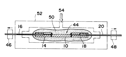
Next, as shown in rig. 5, the module body 44 on
which the resin 50 is applied is placed in a mold 52 of
a molding device while being suspended between the
clamps 46, 48. At this point, the module body 44 is
placed substantially in the center of the space of the
mold 52 and spaced apart from the inner wall surface of
the mold 52. Thereafter, a proper resin 54 is injected
into the mold 52 and cured. The resin 54 must form a
certain shape after cured, and must have the heat
resistance and the moisture resistance. As this sort
of the resin 54, a thermosetting epoxy resin (e. g.,
trade name: EPOTECH product of Epoxy Technology Corp.)
is preferable. When this thermosetting epoxy resin is
used, it is effective that the module is molded in
accordance with the transfer molding. Alternatively,
' an ultra violet ray curing resin (e. g., trade name:
OPTO-DAINE product of DAIKIN Corp.), a silicon resin
(e. g., trade name: Silicone Gel product of Sin-Etsu
Corp.), an urethan resin (e. g., trade name: PEL-
URETHANE product of Nippon Pelnox Corp.) etc. can be
used.
After the resin 54 is cured, the mold 52 is
removed and the clamp members 46, 48 are removed from
the optical fibers 16, 20. There are boot attaching
~13909C~
SEI 94-43
portions 56, 58 (Fig. 1) to which the aforesaid
protecting boots 38, 40 are attached and which are
formed at both ends of the cured resin 54, that is, an
enclosure body 54. When the protecting boots 38, 40
are fitted on the boot attaching portions 56, 58, the
optical device module 100 shown in Fig. 1 is completed.
In the optical device module 100 formed in this
manner, the enclosure body 54 surrounding the module
body 44 is molded with the epoxy resin or the like, so
that the shape of the outer appearance is constant.
Moreover, since the module body 44 is surrounded by the
molded resin 54, the module body 44 is completely
sealed from the external environment. Therefore, the
module~body 44 is protected efficiently from the
external heat, moisture, mechanical shock etc.
Further, since the gel-like resin 50 is interposed
between the module body 44 and the enclosure body 54,
the module body 44 is protected from the external
environment by the resin 50.
The module body 44 is immersed in the gel-like
resin 50, and then flo~.ted and supported inside the
enclosure body 54. Since the resin 50 has the proper
viscosity, if the mechanical shock is applied to the
optical device module 100 from the outside, the shock
is absorbed by the gel-like resin 50. Therefore, the
gel-like resin 50 functions as the cushioning material.
11
X139090
SEI 94-43
Moreover, even though the heat is applied to the
optical device module 100 and the adhesive 42 in the
coupled portion of the module body 44 is thermally
expanded or thermally shrunk, the gel-like resin 50 can
accommodate the movement of the fiber connectors 14,
18.
There is shown in Fig. o ar. optical device module
200 formed in accordance with the second embodiment of
the present invention. The optical device module 200
of the second embodiment is different from the optical
device module of the first embodiment in that the gel-
like resin 50 is not applied onto the whole module body
44. In this case, the gel-like resin 50 is applied
onto the whole first and second fiber connectors and
portions of the waveguide substrate 10 adjacent to
these fiber connectors 14, 18. Since to be influenced
by the external mechanical shock, heat and moisture is
the coupled portions between the fiber connectors 14,
18 and the waveguide substrate 10, and the fiber
connectors 14, 18, if at least these parts are
protected by the gel-like resin 50, the same effect as
in the first embodiment will be attained.
When the urethan resin is used as the gel-like
resin 50, it can be used in the form of a gel. But,
because the cured urethan resin is superior in
elasticity, it can be used as a cushioning material.
12
X139090
SEI 94-43
For this reason, like an optical device module 300
shown in Fig. 7, an enclosure body 60 made of urethan
resin is directly formed around the module body 44.
Fig. 8 shows an optical device module 400 formed
in accordance with the fourth embodiment of the present
invention. In the case of forming the optical device
module 100 of the first embodiment, the module body 44
is supported and suspended by the clamps 44, 46.
However, in the case of the optical device module 400
of the fourth embodiment, without using the clamps, the
bottom surface of the waveguide substrate 10 in the
module body 44 is supported by at least one support
rod.
In detail, after the first and second fiber
connectors 14, 18 are coupled to the waveguide
substrate 10, the gel-like resin 50 is applied onto the
module body 44 except the center portion of the bottom
surface of the waveguide substrate 10. Thereafter, as
shown in Fig. 9, the center portion of the waveguide
substrate 10 rests on an upper end face of a support
rod 62 projecting from the bottom surface of mold 52 of
the molding device. Then, the melting resin 54 such as
the epoxy resin is injected into the mold 52 and cured.
Formed in this manner is the optical device module 400
shown in Fig. 8. In Fig. 8, a hole denoted by the
numeral 64 is formed when the support rod 62 is
13
2139090
SEI 94-43
removed. This hole 64 can be utilized in the various
measurement, for example, the measurement of internal
temperature of the optical device module 400. It
should be noted that since a portion 66 of the
enclosure body 54 surrounding the upper end of the hole
64 is tightly in contact with the bottom surface of the
waveguide substrate 10, water and others do not enter
through the hole 64 ane never reach the fiber
connectors 14, 18.
The preferred embodiments of the present invention
have been described in detail but it is needless to say
that the present invention is not limited to the above
embodiments. For example, the resin composing the
enclosure body of the optical device module and the
gel-like resin are not limited to the above-described
ones but any suitable resins can be used. Further, the
optical device may be the one that an optical component
is placed onto the optical waveguide forming surface of
the waveguide substrate.
As described above, according to the present
invention; almost whole module body is coated with the
integrally molded resin such as epoxy resin, so that
the module body is protected efficiently from the
external heat, moisture, mechanical shock etc. Even
though the adhesives between the fiber connectors and
the optical device are thermally expanded or thermally
14
_ . CA 02139090 2004-08-10
shrunk, the gel-like resin accepts 'the movement of the
fiber connectors. Therefore, the excess force does not
act on the module body.
According to the method of the present invention,
S after the gel-like resin is applied onto the module
body, the enclosure body is formed, e_g., in accordance
with the transfer molding method. Therefore, the
module body is resiliently immersed in the geI-like
resin without any space left.
From the invention thus described, it will be
obvious that the invention may be varied in many ways.
Such variations are not to be regarded as a departure
from the spirit and scope of the invention, and all
such modifications as would be obvious to one skilled
in the art are intended to be included within the scope
of the following claims.