Note: Descriptions are shown in the official language in which they were submitted.
2139151
, `
TWO-DIMENSIONAL ACOUSTIC ARRAY AND
METHOD FOR THE MANUFACTURE THEREOF
FIELD OF THE INVENTION
This invention relates to acoustic transducers
and more particularly to a two-dimensional transducer
array for use in the medical diagnostic field.
BACKGROUND OF THE INVENTION
Ultrasound machines are often used for
observing organs in the human body. Typically, these
machines contain transducer arrays, which are comprised
of a plurality of individually excitable transducer
segments, for converting electrical signals into pressure
waves. The transducer array may be contained within a
~ hand-held probe, which may be adjusted in position to
direct the ultrasound beam to the region of interest.
Electrodes are placed upon opposing portions of the
transducer segments for individually exciting each
segment. The pressure waves generated by the transducer
segments are directed toward the object to be observed,
such as the heart of a patient being examined. Each time
the pressure wave confronts an interface between objects
having different acoustic characteristics, a portion of
the pressure wave is reflected. The array of transducers
may receive and then convert the reflected pressure wave
into a corresponding electrical signal.
2139151
.
-- 2 --
Two-dimensional transducer arrays are desirable
in order to allow for increased control of the excitation
along an elevation axis, which is otherwise absent from
conventional single-dimensional arrays. A two-
dimensional transducer array has at least two transducer
segments arranged along each of the array's elevation and
azimuthal axes. Typically in a two-dimensional
transducer array there are 128 transducer segments along
the array's azimuthal axis and two or more segments along
the array's elevation axis. As a result of the two-
dimensional geometry, one is able to control the scanning
plane slice thickness for clutter free imaging and better
contrast resolution.
It is desirable to form high density two-
dimensional transducer arrays because they are compact
and may provide clearer images. However, prior art high
density two-dimensional arrays are typically difficult to
fabricate because the width of the transducer elements is
generally 50 to 100 ~m. In order to produce a high
density two-dimensional transducer array, many leads or
traces are soldered to the small individual transducer
segments in the array in order to provide the appropriate
electrical signals for excitation. Thus, on a typical
two-dimensional transducer array, hundreds of traces must
be soldered to the respective segments to effect
excitation.
213glSl
- ~ j
As a result of the high density form of the
arrays, prior art two-dimensional transducer arrays
typically have unreliable lead attachments to the
respective transducer segments. The dimensions of the
segments are small and the connections between the traces
and the transducer segments may fail. In addition, the
traces and solder connections are subject to heating and
cooling and may not withstand the temperature changes.
As a result, these connections may break apart. Yields
as low as 10 percent for producing high density two-
dimensional arrays are not uncommon. Consequently, prior
art methods for constructing high density two-dimensional
transducer arrays have generally been complex,
unreliable, and cost prohibitive from a yield point of
view.
In addition to the problem of unreliable lead
attachments, typical prior art transducers operating at
higher frequencies with the larger elevation aperture of
the two-dimensional array will clutter imaging in the
shallow portions of the human body. It is desirable to
image regions deep within the human body at higher
frequencies, while maintaining the ability to generate
clear near-field images. Generally, higher frequency
transducer arrays having a smaller elevation aperture are
used to improve the resolution of sectional plane images
of shallow regions within the human body.
2139151
Higher ultrasonic frequencies, however, are
more quickly attenuated in the human body. Therefore, in
conventional ultrasound systems, lower frequencies of
ultrasonic waves are generally used to improve the
resolution of sectional plane images of deeper regions
within the human body. Nonetheless, clearer images of
deeper regions within the human body may be generated if
the transducer array is capable of providing higher
ultrasonic frequencies from an expanded or larger
elevation aperture while also being capable of
maintaining clutter free near field images. Clutter free
near field images may be produced if the same transducer
array is capable of providing higher ultrasonic
frequencies from a smaller elevation aperture (i.e.,
switching-in a smaller elevation aperture).
SUMMARY OF THE INVENTION
There is provided in a first aspect of this
invention a two-dimensional array for use in an acoustic
imaging system which comprises a plurality of transducer
segments each having a trace for exciting an electrode on
each of the transducer segments, the trace and the
electrode being formed of the same material.
According to a second aspect of this invention,
there is provided a two-dimensional array for use in an
acoustic imaging system which comprises a plurality of
transducer segments, each of the segments having a first
21391Sl
, ~,
piezoelectric portion, a second piezoelectric portion, a
first electrode, a second electrode and a third
electrode. The first piezoelectric portion is disposed
on the first electrode, the second electrode is disposed
between the first piezoelectric portion and the second
piezoelectric portion. The second electrode has a trace
for electrically exciting the segment, the second
electrode and the trace forming a one-piece member.
Further, the third electrode is electrically connected to
an opposing surface of the second piezoelectric portion.
According to a third aspect of this invention,
there is provided a two-dimensional array for use in an
acoustic imaging system which comprises an
interconnecting circuit having a first plurality of
traces extending along a first side and a second
plurality of traces extending along a second opposing
side. A piezoelectric layer is disposed on the
interconnecting circuit, the interconnecting circuit and
piezoelectric layer being diced to form individual
transducer segments. Further, an electrode layer is
electrically connected to the piezoelectric layer.
According to a fourth aspect of this invention,
there is provided a two-dimensional array which comprises
at least two transducer segments arranged along an
elevation direction, each of the transducer segments
having a trace for exciting an electrode on each of the
" 21391~1
transducer segments, the trace and electrode being a one-
piece member.
A first preferred method of constructing a two-
dimensional transducer array comprises the steps of
disposing an interconnecting circuit on a support
structure having a first plurality of traces extending
along one side of the support structure and a second
plurality of traces extending along a second opposing
side of the support structure, placing a piezoelectric
layer on the interconnecting circuit, dicing the
piezoelectric layer and interconnecting circuit to form a
plurality of transducer segments, and disposing an
electrode layer on the diced transducer segments. Each
of the segments is electrically coupled to one of the
traces.
A second preferred method of constructing a
two-dimensional transducer array comprises the steps of
disposing an electrode layer on a support structure
having a first and an opposing second side, disposing a
piezoelectric layer on the electrode layer, disposing an
interconnecting circuit on the piezoelectric layer having
a first plurality of traces extending along the first
side of the support structure and a second plurality of
traces extending along the second side of the support
structure, and dicing the piezoelectric layer and the
interconnecting circuit to form a plurality of transducer
2139151
,
segments. Each of the segments are electrically coupled
to one of ~he traces.
BRIEF DESCRIPTION OF THE DRAWINGS
FIG. l(a) is a perspective view of a flexible
circuit placed over a backing block forming an assembly
and FIG. l(b) further has a piezoelectric layer and
matching layer disposed on the assembly.
FIG. 2 is a perspective view of a first
embodiment of the two-dimensional acoustic array of the
present invention employing a single crystal design
having a matching layer, and having two transducer
segments in the elevation direction.
FIG. 3 is a cross-sectional view of the
acoustic array of FIG. 2 taken along the lines 3-3 and
also illustrating a mylar shield ground return.
FIG. 4 is a perspective view of a second
embodiment of the two-dimensional acoustic array of the
present invention employing a single crystal design
having a matching layer, and having three transducer
segments in the elevation direction.
FIG. 5 is a cross-sectional view of the
acoustic array of FIG. 4 taken along the lines 5-5 and
also illustrating the mylar shield ground return.
FIGS. 6(a) and (b) are beam profiles showing
~ performance of the transducer design of FIG. 4 by firing
21~9151 i
-- 8 --
only the center segment in the near field and firing the
full aperture in the far field.
FIG. 7 is a cross-sectional view of a third
embodiment of the present invention employing a single
crystal design having two-segments in the elevation
direction and having a flexible circuit disposed under a
matching layer.
FIG. 8 is a cross-sectional view of a fourth
embodiment of the present invention employing a two
crystal design having a matching layer and three segments
in the elevation direction.
FIG. 9 is an enlarged view of the connection
between the two backing blocks of FIG. 8 and also
illustrating the mylar shield ground return.
FIG. 10 is a cross-sectional view of 2 fifth
embodiment of the present invention employing a two
crystal design having a matching layer and two segments
in the elevation direction.
DESCRIPTION OF THE PREFERRED EMBODIMENTS
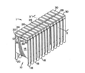
Referring now to FIGS. 2 and 3, there is
provided a high density two-dimensional acoustic array
in accordance with a first preferred embodiment of the
present invention. Referring also to FIG. l(a), a first
assembly 10 consists of an interconnecting circuit or
flexible circuit 12 and a support structure or backing
block 14. The backing block 14 serves to support the
2139151
. ~
.
transducer structure. Although the upper surface of the
backing block 14 supporting the transducer structure is
shown to have a flat surface, this surface may comprise
other shapes, such as a curvilinear surface. The
flexible circuit 12 will eventually serve to provide the
respective signal electrodes and corresponding traces or
leads once the flexible circuit 12 is severed, as will be
described. The first assembly 10 is also used to
construct other embodiments of this invention.
Flexible circuit 12 has a center pad 16 which
is disposed on the backing block 14. As shown in FIGS. 1
through 3, the flexible circuit 12 has a plurality of
adjacent traces or leads 18 and 20 extending from
opposing sides of the center pad 16. The flexible
- 15 circuit 12 is typically made of a copper layer bonded to
a piece of polyimid material, typically KAPTON-.
Flexible circuits such as the flexible circuit 12 are
manufactured by Sheldahl of Northfield, Minnesota.
Preferably, the flexible circuit thickness is
approximately 25~m for a flexible circuit manufactured by
Sheldahl.
Of course, materials other than the copper
layer and polyimid material may be used to form the
flexible circuit 12. The flexible circuit may comprise
any interconnecting design used in the acoustic or
integrated circuit fields, including solid core,
stranded, or coaxial wires bonded to an insulating
2139151
. ~
-- 10 --
material, and conductive patterns formed by known thin
film or thick film processes. In addition, the material
forming the backing block 14 is preferably acoustically
matched to the flexible circuit 12, resulting in better
performance. Further, the acoustic impedance of the
flexible circuit is approximately equal to that of the
epoxy material for gluing the flexible circuit 12 to the
backing block 14, which is described later.
As shown in FIGS. l(b), 2 and 3, a
piezoelectric layer 22 is disposed on the center pad 16
of the flexible circuit 12 of the first assembly 10. In
addition, an acoustic matching layer 24 may then be
disposed on the piezoelectric layer 22 to further
increase performance.
The piezoelectric layer 22 may be formed of any
piezoelectric ceramic material such as lead zirconate
titanate (PZT) or lead meaniobate. In addition, the
piezoelectric layer 22 may be formed of composite
material such as the composite material described in R.E.
Newnham et al. "Connectivity and Piezoelectric-
Pyroelectric Composites", Materials Research Bulletin,
Vol. 13 at 525-36 (1978) and R.E. Newnham et al.,
"Flexible Composite Transducers", Materials Research
Bulletin, Vol. 13 at 599-607 (1978). Alternatively, the
piezoelectric layer 22 may be formed of polymer material
polyvinylidene fluoride (PVDF).
2139151
11 --
The backing block may be formed of a filled
epoxy comprising Dow Corning's part number DER 332
treated with Dow Corning's curlng agent DEH 24 and has an
aluminum oxide filler. In addition, preferably the
matching layer is formed of a filled polymer. The
matching layer may be coated with electrically conductive
materials, such as nickel and gold.
Preferably, the backing block 14, the flexible
circuit 12, the piezoelectric layer 22, and the matching
layer 24 are glued to one another in one step by use of
an epoxy adhesive. The epoxy adhesive is placed between
the backing block 14 and the flexible circuit 12, between
the flexible circuit 12 and the piezoelectric layer 22,
and between the piezoelectric layer 22 and the matching
layer 24. These layers are secured to one another by
fixturing all layers together and applying pressure to
the layers. Preferably, 60psi is applied in oràer to
secure the layers together.
Alternatively, the layers may be glued to one
another at different stages (i.e., the flexible circuit
may first be glued to the backing block and in a separate
step, the piezoelectric layer is later secured to the
flexible circuit). However, this increases the time for
securing the layers to one another.
An epoxy of HYSOL~ base material number 2039
having a HYSOL~ curing agent number HD3561, which is
manufactured by Dexter Corp., Hysol Division of Industry,
.~ 2139151
~, ~
.
- - - 12 -
California, may be used for gluing the various materials
together. Preferably, the thickness of the epoxy
material is approximately 2~m or less.
As shown in FIG. 2, the center pad 16 of the
flexible circuit 12, the piezoelectric layer 22 and the
acoustic matching layer 24 are diced by forming kerfs 26
and 28 therein with a standard dicing machine. Kerfs 26,
which are parallel to the elevation axis of the array 1,
are located between adjacent traces 18 and adjacent
traces 20. Preferably, the kerfs 26 are formed by dicing
between adjacent traces 18 and 20 starting at one end of
the array 1 and making parallel kerfs until reaching the
other end of the array. The kerf 28 may be located
parallel to the azimuthal axis of the array, preferably
equidistant between the traces 18 and the traces 20, as
shown in FIGS. 2 and 3. The kerfs 26 and 28 may extend a
short distance into the backing block 14. Since the
backing block 14 is not substantially cut (i.e., 5 to 10
thousandths of an inch in depth), piezoelectric layer 22
and acoustic matching layer 24 are still supported by the
backing block 14.
As a result of the dicing operation, transducer
segments 30 are formed, each segment 30 having an
electrode 32, a piezoelectric portion 34 and an acoustic
matching layer portion 36. The electrode 32, the
piezoelectric portion 34, and the acoustic matching layer-
portion 36 are preferably coextensive in size along the
~_ 213~151
.
- - 13 -
azimuthal and elevation axes. Further, the traces 18 and
20 have a width which is substantially coextensive in
size with a width of the electrode 32.
It is preferable that the traces 18 are aligned
with the traces 20 parallel to the elevation axis of the
array 1. This permits all transducer segments 30
arranged parallel to the elevation axis of the array 1 at
a given azimuthal position to be cut at the same time by
forming a single kerf 26. However, the traces 18 do not
have to line up with the traces 20 to practice the
invention. If the traces 18 are not aligned with the
traces 20, additional dicing may be required. That is,
dicing should be performed in a region between adjacent
traces 18 and adjacent traces 20 in order to form the
-~ 15 respective transducer segments.
An electrode or layer 38 may be placed over the
acoustic matching layer portions 36, as shown in FIG. 3.
The electrode 38 may be at common ground or alternatively
at any appropriate reference potential. The electrode 38
is preferably a 12.5 ~m MYLAR electrode coated with 2000-
3000 A of gold. The gold coating is placed on the MYLAR
layer by use of sputtering techniques. This gold coating
is preferably in contact with the matching layer portions
36 and may be applied by sputtering prior to applying the
MYLAR layer. Further, 500 A of chromium may be sputtered
on the MYLAR layer prior to sputtering the gold coating
213`~151
.
- 14 -
in order to allow the gold coating to better adhere to
the MYLAR layer.
The matching layer portions 36 are preferably
electrically coupled to the electrode 38 via a
metalization layer across the four edges of the matching
layer portion. That is, both the upper surface and the
four side edges of the matching layer portion are coated
with electrically conductive material, shorting the
electrode 38 to the respective piezoelectric portions 34.
An electrically conductive matching layer material such
as magnesium or a conductive epoxy may be used to short
the electrode 38 to the piezoelectric portion 34. This
results in an electroded acoustic matching layer.
Because the flexible circuit 12 is diced as
described above, the center pad 16 of the flexible
circuit 12 is formed into an individual electrode 32 for
each of the transducer segments 30. The individual
electrodes 32 electrically couple the signal for exciting
the respective transducer segments 30 from the traces 18
and the traces 20, which are automatically and integrally
formed with the respective electrodes 32 because of the
dicing process. For a given transducer segment 30, the
trace 18 or 20 and the electrode 32 are a one-piece
member and are formed of the same material. However, the
electrode 32 and trace 18 or 20 may be formed by other
methods. For example, if the~electrode 32 and trace 18
or 20 were formed by a thin film process on a composite
2139151
. ` . .
s -- 15 --
ceramic material, there would be no need to dice between
adjacent electrodes 32. Ir. addition, there are two
electrodes 32 and 38 for exciting a given transducer
segment 30.
Referring to FIGS. 4 and 5, there is provided a
second embodiment of the present invention where like
components are labeled similarly to the first embodiment.
Rather than having two transducer segments 30 arranged
along the elevation direction, the second embodiment has
three transducer segments 30a, 30b, and 30c arranged
along the elevation direction. It is desirable, although
not necessary to practice this invention, to have an odd
number of transducer segments 30 arranged along the
elevation direction for symmetry of construction.
,.~,J 15 Symmetry of construction is desirable because
it allows focusing from a point in the near field to a
point in the far field along the same scanning line
without the need to otherwise shift the position of the
transducer. When focusing in the near field, only the
center segment is activated. When focusing in the far
field, segments equidistant from the center segment are
activated as well. Were the transducer to have an even
number of-segments, it may be necessary to reposition the
transducer in order to effect focusing at a different
point for a given scan line.
A joined assembly 50 is formed by severing the
first assembly 10 of FIG. l(a), forming a severed
213glSl
- 16 -
assembly 40, and bonding the severed assembly 40 to a
second asse...bly 46 along bonding region 48. The first
assembly 10 is severed along the longitudinal direction
4-4, shown in FIG. l(a), to form the severed assembly 40,
as shown in FIGS. 4 and 5. Preferably, the first
assembly 10 is severed approximately along the line
through the center pad 16 that is equidistant from the
traces 18 and the traces 20. The severed assembly 40
contains the remaining backing block 42, the remaining
flexible circuit 44 having remaining traces 45. The
second half of the first assembly 10 may be discarded or
used for constructing a second transducer array assembly.
The second assembly 46 is similar in
construction to the first assembly 10 of FIG. l(a).
Preferably, the dimensions of the first assembly lO and
second assembly 46 are identical. The severed assembly
40 is bonded to the second assembly 46 by use of an epoxy
adhesive, such as the HYSOL~ epoxy adhesive described
earlier.
A piezoelectric layer 22 is disposed on the
joined assembly 50. An acoustic matching layer 24 may
also be disposed on the piezoelectric layer 22. As
described with regard to the two-dimensional array of
FIG. 2, all of the gluing between layers as well as the
gluing of the severed assembly 40 to the second assembly
-46 are preferably performed in one step. Further, it is
preferable to make sure that adjacent traces 20 line up
~ 2139151
- 17 -
,with adjacent traces 18 and adjacent traces 45. This
allows dicing at a given point along the azimuthal
direction to be accomplished by one cut rather than a
series of cuts.
It is preferable that the traces 18, 20, and 45
be aligned parallel to the elevation axis of the array.
In order to help align the traces, tooling holes, not
shown, may be placed along extensions, not shown, of the
center pad 16 which extend in the azimuthal direction
beyond both longitudinal ends of the backing block 14.
Preferably, there are two such tooling holes at each end
of the center pad 16 of the first assembly shown in FIG.
l(a). When the severed assembly 40 is formed, one
tooling hole at each end of the extensions of the center
pad 16 remains on the remaining flexible circuit 44.
Further, the second assembly 46 has two tooling holes at
each end. As a result, an operator may align the traces
45 of the severed assembly 40 with the traces 18 and the
traces 20 of the second assembly 46.
As with the first embodiment, a dicing machine
is then used to dice the center pad 16 of the flexible
circuit 12, the remaining flexible circuit 44,
piezoelectric layer 22 and acoustic matching layer 24.
As described earlier, the kerfs extend only a short
distance into the backing blocks. Dicing occurs between
adjacent traces 20, 18, and 45.
~_ , 2139151
.
- 18 -
A kerf 52 may be formed in a region of the
remaining flexible circuit 44, piezoelectric layer 22,
and acoustic matching layer 24 disposed approximately
above the bonding region 48 between the severed assembly
40 and the second assembly 46. Preferably, the kerf 52
is formed along the severed edge of the severed assembly
40, beginning in the elevation direction just far enough
away from the traces 18 so as not to cut through or
disturb the flexible circuit 12, as best seen in FIG. 5.
The kerf 52 should cut through the remaining flexible
circuit 44 to ensure isolation between the remaining
flexible circuit 44 and flexible circuit 12.
Alternatively, the first assembly 10 may be severed such
that the remaining flexible circuit 44 is isolated from
flexible circuit 12 when the severed assembly 40 and the
second assembly 46 are joined, i.e., the remaining
flexible circuit 44 is cut where the kerf 52 would
otherwise extend into remaining flexible circuit 44, so
that there is no need for the kerf 52 to also sever the
remaining flexible circuit 44.
Another kerf 54 is placed in a region of the
flexible circuit 12, piezoelectric layer 22, and acoustic
matching layer 24 above the second assembly 46,
preferably near the longitudinal center line of the
second assembly 46. Thus, individual transducer segments
30a, 30b, and 30c are formed. That is, for a given
azimuthal position, three segments 30a, 30b, and 30c are
2139151
. ~'.
.
- 19 -
formed along the elevation direction each having an
electrode 32 with a trace 18, 20, or 45 integral
therewith, a piezoelectric portion 34, and an acoustic
matching layer portion 36. A common ground electrode 38
may be placed over the acoustic matching layer 36.
The traces 18, 20, and 45 may then be connected
to the external circuitry for exciting the individual
transducer segments 30a, 30b, and 30c. Preferably, the
traces 20 and 45 for a given azimuthal position may be
electrically connected by wire 56. A nosepiece or
enclosure is placed around the transducer structure.
This nosepiece may have a hole where a cable may be
inserted, providing the electrical wires from the
acoustic imaging system for exciting each of the
respective transducer segments 30a, 30b, and 30c.
As with the first embodiment, because the
flexible circuits 12 and 44 are diced as described above,
the traces 18, 20, and 45 coupled to the respective
transducer segments 30a, 30b, and 30c are automatically
formed and are each integrally connected with the
electrode 32 which is formed. The respective electrode
32 and trace 18, 20 or 45 form a one-piece member of the
same material. In addition, the electrode 32 is
coextensive in size with the piezoelectric portion 34
along the azimuthal and elevation axes. Thus, a
dependable connection is made from each trace 18, 20, or
45 feeding the signal to the appropriate electrode 32, as
~_ 2139151
.
- 20 -
well as between the electrode 32 and the piezoelectric
portion 34 of the respective transducer segment 30a, 30b,
and 30c. In order to further increase electrical
coupling between the flexible circuits 12 and 44 and the
respective transducer piezoelectric portion 34, the
flexible circuits may be gold plated.
When forming a transducer array 1 having three
segments along the elevation direction, as shown in FIG.
4, the dimension of the backing block 14 preferably is
1.5cm in the elevation direction, 2.5cm in the azimuthal
direction, and 2cm in the range direction. In addition,
the center pad 16 preferably is coextensive in size with
the backing block 14 along the azimuthal and elevation
axes. The traces 18, 20 and 45 preferably have a width
19, shown in FIG. 1, of 50 to 100 ym. In addition, the
spacing between the traces are typically one-half to two
times the wavelength of the operating frequency in the
body being examined.
Further, the dimension of the piezoelectric
layer 22 for the construction shown in FIG. 4 is
preferably 1.5cm in the elevation direction, 2.5cm in the
azimuthal direction, and 0.25mm in the range direction.
The dimension of the matching layer 24 is preferably
1.5cm in the elevation direction, 2.5cm in the azimuthal
direction, and 0.125mm in the range direction. The kerfs
26 are preferably approximately 50.8 ~m in width. The
kerfs 52 and 54 are preferably 101.6 ~m in width.
~, 213gl51
- ; :
FIG. 6 illustrates a beam profile in accordance
with the principles of this invention. FIG. 6(a)
illustrates beam 68 which is the beam profile for
focusing in the near field where only the center
transducer segments 30a of the two-dimensional array 1
are activated for the construction shown in FIG. 4. The
range of utilization 67 is 0 to approximately 5 to 6 cm.
In addition, the aperture width 69 of the exiting beam is
approximately 5mm. FIG. 6(b) illustrates beam 70, which
is the beam profile for focusing in the far field. The
range of utilization 72 is approximately 5cm to 20cm.
Further, the aperture width 71 of the exiting beam is
approximately 15mm. In the far field, the full aperture
is activated, resulting in more energy for larger depth
;~ 15 of penetration. Because the aperture may be expanded
when focusing in the far field, higher frequency imaging
can be achieved without sacrificing near field image
quality. Thus, clearer images may be produced.
Although FIGS. 4 and 5 show a single second
assembly 46 being combined with a single severed assembly
40, additional severed assemblies 40 may be appropriately
bonded to the joined assembly 50. Thus, four or more
transducer segments 30 may be provided along the
elevation axis. Preferably, an odd number of transducer
segments 30 are provided in the elevation direction for
symmetry of construction. Should an odd number of
transducer segments 30 be chosen, then segments
~, 2139151
.
- 22 -
equidistant from the center segment may be electrically
connected, as shown by the wire 56 in FIG. 5. Further;
one or more joined assemblies 50 may be combined if the
traces at the binding region are appropriately
electrically isolated from one another.
For example, if a high density two-dimensional
array 1 is employed having five transducer segments 30 in
the elevation direction, then the outer two segments may
be electrically joined together and the second and fourth
segments may be electrically joined together. In order
to form such a construction, two severed assemblies 40
may be bonded at each end of the construction shown in
FIG. 4 whereby each of the traces 45 for a given severed
assembly 40 is placed on the side opposing the bonding
region 48.
Although with the configurations shown in FIGS.
1 through 5, the flexible circuit 12 lies below the
electrode layer 38, the electrode layer may be placed
directly above the backing block, as shown in FIG. 7. In
this alternate embodiment, the piezoelectric layer 22 is
placed above the electrode layer 38, the center pad 16 of
the flexible circuit 12 is placed above the piezoelectric
layer 22, and an acoustic matching layer 24 may be
disposed upon the center pad 16 of the flexible circuit
12 if a matching layer is used. The width of the
electrode 38, the piezoelectric layer 22, and the
matching layer 24 are preferably 0.5mm shorter at each
~ 2139151
,
- 23 -
end of the backing block. This will later allow for
electrical isolation between the electrodes to be formed.
As described earlier, the ground layer may be at common
ground or any appropriate reference potential and the
acoustic matching layer may be an electroded acoustic
matching layer.
When dicing the assembly to form the individual
transducer segments 30, only the flexible circuit 12, the
acoustic matching layer 24, and the piezoelectric layer
22 would be severed. The kerfs would not necessarily
extend into the common ground electrode or the backing
block. As a result,` a top electrode would couple the
excitation signal to a corresponding transducer segment
from a trace which is formed of the same material as that
respective top electrode, forming a one-piece member.
Further, an array with three segments 30 in the elevation
direction may be constructed from a first assembly joined
to a second assembly, as previously described with
respect to FIGS. 4 and 5, wherein the cross-section of
each transducer segment is as shown in FIG. 7.
Now referring to FIGS. 8 and 9, there is shown
an alternate embodiment for a two crystal design 60
wherein like components are labeled similarly. The two
crystal design differs from the single crystal design
shown in FIGS. 2 through 5 in that a first ground layer
62 is placed above the backin-g block 14 and a first
piezoelectric layer 64 is disposed above the ground layer
~ ~ 21391~1
,
- 24 -
62. Thus, referring also to FIG. l(a), both a ground
layer 62 and a first piez~electric layer 64 would be
placed above backing block 14 and below the center pad 16
of flexible circuit 12, forming a first assembly 10. The
width of the first ground layer 62 and the first
piezoelectric layer 64 are preferably 0.5mm shorter at
each end of the backing block 14. This will later allow
for electrical isolation between the electrodes to be
formed. This first assembly 10 is severed as was done
with the single crystal design, forming a severed
assembly 40. The severed assembly 40 is bonded to a
second assembly 46 preferably having similar dimensions
to the first assembly 10 along bonding region 48.
As with the embodiments of FIGS. 4 and 5, a
second piezoelectric layer 22 is disposed above the
joined assembly 50. To further increase performance, an
acoustic matching layer 24 may also be disposed above the
second piezoelectric layer 22. Then, as before, the
joined assembly is diced in the azimuthal direction with
kerfs between the adjacent traces 18, 20, and 45. The
layers and assemblies are bonded together as described
earlier.
Once the dicing is complete, a kerf 52 may
sever the acoustic matching layer 24, second
piezoelectric layer 22, remaining flexible circuit 44,
first piezoelectric layer 64 and ground layer 62. This
ensures that the segments to be formed (i.e., the
~ 2139151
.
S - 25 -
segments above the remaining backing block 42) are
electrically isolated from the adjacent segments along
the elevation direction. The kerf 52 is parallel to the
azimuthal axis and, as described in regard to FIG. 5, is
located above the bonding region 48 between the severed
assembly 40 and the second assembly 46.
Another kerf 54 may also be placed in a region
above the second assembly 46, preferably near the
centerline of the second assembly. The kerf 54 should
cut acoustic matching layer 24 into matching layer
portions 36, second piezoelectric layer 22 into
piezoelectric portions 34, flexible circuit 12 into
electrodes 32 having traces 18, 20 integral therewith,
and first piezoelectric layer into first piezoelectric
portions 66 and electrode layer 62 into electrodes 63.
Once this is complete, a mylar shield ground return 38,
as described earlier, may be placed above the acoustic
matching layer portions 36. This ground return 38 is
electrically connected to ground layers 62. The two
crystal design results in a more sensitive transducer
probe.
In a preferred operation of the two-dimensional
array shown in ~IGS. 4 and 8, the transducer array 1 may
first be operated at a higher frequency (e.g., 5 MHz)
along a given scan line in order to focus the ultrasound
~ beam at a point in the near field. When imaging in the
near field, typically one to six centimeters in depth of
`-` 21391~1
. - .
- 26 -
the object of interest, only the center segments 30a of
the array 1 are activated. Thus, an excitation signal is
provided to traces 18. As the transducer array 1 is
gradually focused along successive points along the scan
line, the outer segments 30b and 30c may also be
activated. An excitation signal is provided to traces
18, 20, and 45. Thus, the elevation aperture is expanded
and more energy penetrates into the body, producing
clearer images in the far field. When using the
embodiment shown in FIGS. 4 and 8,.it is preferable that
the outer traces for a given azimuthal position be
connected by the wire 56 in order to simplify
construction. Thus, only one electrical signal is
required to activate an outer segment 30b and a
~- 15 corresponding outer segment 30c when focusing in the far
field.
It should be noted that even though a two-
crystal design was shown in FIGS. 8 and 9 having three
segments in the elevation direction, a two-crystal design
having two segments may be provided, as illustrated in
FIG. 10. With such a construction, the severed assembly
40 would not be bonded to the second assembly 46.
Rather, the piezoelectric layer 22 and acoustic matching
layer 24 would be placed directly on the flexible circuit
12, dicing between the adjacent traces 18 and 20, and
placing the kerf 54 in a region above backing block 14.
Should more than three segments be required along the
~ 213gl51
elevation axis, then the appropriate number of severed
assemblies 40 may be bonded on each side of the second
assembly 46, placing a kerf 52 for each severed assembly
employed above the bonding region 48. In addition, each
of the embodiments described may be used with
commercially available units such as Acuson Corporation's
128 XP System having acoustic response technology (ART)
capability.
It is to be understood that the forms of the
invention described herewith are to be taken as preferred
examples and that various changes in the shape, size and
arrangement of parts may be resorted to, without
departing from the spirit of the invention or scope of
the claims.