Note: Descriptions are shown in the official language in which they were submitted.
CA 021392~9 1998-03-10
NE-638
TITLE OF THE INVENTION
2 "DS/CDMA Receiver Using Parallel-Operating Multi-Purpose Correlators"
3 BACKGROUND OF THE INVENTION
4 Field of the Invention
The present invention relates generally to direct sequence spread
6 spectrum (code division multiple access) receivers. This invention is
7 particularly concerned with a sync acquisition and tracking technique for
8 direct sequence spread spectrum receivers of cellular mobile
9 communications systems in which transmitted signals are severely
10 affected by Rayleigh fading and multipath fading.
11 Description of the Related Art
12 Commercial interest in direct sequence spread spectrum (code
13 division multiple access) communication systems has recently risen due to
14 their potential ability to provide service to more users than is offered by
15 other multiple access techniques. In the cell-site station of the DS/CDMA
16 system, a data symbol is spread by multiplying it with orthogonal
17 pseudo-random number (PN) sequences assigned to the cell site as well
18 as with orthogonal Walsh codes assigned to the channel over which the
19 spread signal is transmitted. In order to enable the mobile station to
20 provide sync acquisition and tracking operation, a pilot signal is
21 superimposed on the data symbol sequence. At the mobile station, a
22 sliding correlation technique is used to shift the phase timing of a local PN23 sequence by a predetermined amount each time a correlation is taken
24 between the received and local sequences and determine the correct
25 phase timing for the local sequence when the correlation exceeds some
26 critical value. Such phase shifting is performed at predetermined
27 "window" intervals. Once synchronization is established, the phase
28 difference is monitored and maintained to within one half of the chip
29 interval. During transmission, the signal undergoes reflections from
30 various land structures, producing a complex pattern of standing waves
CA 021392~9 1998-03-10
NE-638
due to mutual interference. As a result, the propagation path of the
2 signal exhibits a field intensity distribution which is approximated by the
3 Rayleigh distribution. Thus, the signal experiences a phenomenon called
4 "Rayleigh fading" and the envelope of the signal at the mobile station as
s well as its phase violently fluctuate.
6 Under such unfavorable conditions, the sliding correlation
7 technique is not ideal to achieve quick synchronization in response to the
8 rapidly varying signal levels. In addition, there is often a need to update
9 the mobile's phase timing due to the arrival of a strong reflection or a
10 signal of significant level from an adjacent cell site. Under such
11 circumstances, the prior art system sets the correlation circuitry to the new2 phase timing immediately in response to the arrival of a new strong signal
13 without taking the old symbols, which may be left in the correlation
14 circuitry, into account. The use of the old symbols for the new phase
15 timing results in timing discontinuity and produces over-correlation or
16 under-correlation.
17 SUMMARY OF THE INVENTION
18 The primary object of the present invention is therefore to
19 provide a direct sequence spread spectrum receiver capable of
20 establishing quick synchronization under varying signal levels.
21 Another object of the present invention is to provide a direct
22 sequence spread spectrum receiver which ensures seamless transition
23 when updating the phase timing of correlation process.
24 According to the present invention, there is provided a direct
25 sequence spread spectrum receiver which comprises a plurality of
26 correlators for despreading a spread data signal and a spread pilot signal,
27 a plurality of pilot demodulators, a plurality of data demodulators and an
28 adder. The data demodulators and the adder constitute a RAKE receiver.
29 During a sync acquisition mode, the pilot demodulators are connected to
30 the correlators, respectively, and during a subsequent tracking mode, the
CA 02l392~9 l998-03-lO
NE-638
data demodulators are connected to the correiators to produce a
2 plurality of demodulated data signals which are combined by the adder
3 to produce an output for the RAKE receiver. A plurality of despreading
4 codes of different phase positions are generated and supplied to the
correlators, respectively, causing the correlators to despread one of the
6 spread data and pilot signals. During the sync acquisition mode, the
7 phase position of each despreading code is successively shifted and high
8 correlation values are determined from the outputs of the pilot
9 demodulators. During the tracking mode, the phase positions of the
despreading codes are set according to the high correlation values. Since
11 multiple correlators operate in parallel during the sync acquisition mode,
12 the time taken to search through the range of possible phase positions is
13 significantly reduced. In practical aspect, the data demodulators are
14 provided in number corresponding to the number of multipath fading
1 s channels.
16 The despreading codes are generated such that, during the sync
17 acquisition mode, all the correlators provide correlations for the incoming
18 pilot signal only, and during the tracking mode, one half of the
19 correlators provide correlation for the data signal and the remainder
provides correlation for the pilot signal.
21 The despreading code comprises a pseudo-random number
22 (noise) sequence uniquely identifying a cell site area and a Walsh code
23 identifying a communication channel. When the Walsh code is set to an
24 all-zero code, the correlators supplied with this code is set to provide
correlation with the pilot signal.
26 In a preferred aspect, a second despreading code of different
27 phase position is supplied to a specified one of the correlators during the
28 tracking mode to continue searching for best phase positions. The phase
29 position of the second despreading code is shifted in the neighborhood
3 0 of those previously set in the sync acquisition mode and high correlation
CA 021392~9 1998-03-10
NE-638
values are newly determined from output signals from one of the pilot
2 demodulators. The previously set phase positions are updated
3 according to the new high correlation values during an update mode.
4 To ensure smooth transition when new phase positions are
determined and old phase positions are to be updated, a second data
6 demodulator is provided. This data demodulator is connected to the
7 output of the specified correlator at the time the specified correlator is set
8 to a new phase position. In response to the connection of the second
9 data demodulator to the specified correlator, a ramp-up time is
introduced to allow old symbols to be replaced with new symbols, and
11 immediately following the ramp-up time, a successive one of the outputs
2 of the other data demodulators is disconnected from the adder for a
13 predetermined interval and, instead, the output of the second data
14 demodulator is connected to the adder during that predetermined
1 s interval.
16 BRIEF DESCRIPTION OF THE DRAWINGS
17 The present invention will be described in further detail with
18 reference to the accompanying drawings, in which:
19 Fig. 1 is a block diagram of a direct sequence spread spectrum
receiver according to the present invention;
21 Fig. 2 is a circuit diagram of each correlator of Fig. 1;
22 Figs. 3A, 3B and 3C are block diagrams of the processor Fig. 1
23 during sync acquisition, tracking and update modes, respectively;
24 Fig. 4 is a circuit diagram of each pilot demodulator of Figs. 3A,
3B and 3C;
26 Figs. 5A and 5B are circuit diagrams of different embodiments of
27 each data demodulator of Figs. 3A, 3B and 3C; and
28 Figs. 6A, 6B and 6C are block diagrams of the phase shift
29 controller Fig. 1 during sync acquisition, tracking and update modes,
respectively.
3 1 DETAILED DESCRIPTION
CA 021392~9 1998-03-10
NE-638
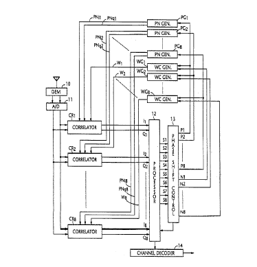
Referring now to Fig. 1, there is shown a receiving circuit of a
2 mobile station for a DS/CDMA cellular communications system according
3 to the present invention. At a cell-site station, a baseband downlink (cell-4 to-mobile) signal is initially encoded by a channel encoder into a known
s coded form that is optimized for radio transmission. At the chip rate
6 much higher than the symbol rate, the symbols of the encoded signal
7 are spread with PN (pseudo-random number) spreading sequences PN
8 and PNq commonly assigned to the service area in which the mobile
9 station is currently located and further spread with orthogonal Walsh
codes uniquely assigned to the downlink channel. A pilot signal, which
11 may be a series of all zeros or ones, is spread at the same chip rate with
12 the same PN sequences PNj and PNq with orthogonal Walsh all-zero
3 codes. The in-phase and quadrature components of spread spectrum
14 downlink signal are combined with the corresponding components of
spread spectrum pilot signal to produce an I signal and a Q signal which
16 are modulated onto orthogonal radio-frequency carriers, amplified and
17 transmitted.
18 The spread spectrum signal from the cell-site is received by the
19 mobile station and supplied to a quadrature demodulator 10 which
includes radio-frequency amplification and demodulation stages. Using
21 orthogonal local carriers, the demodulator 10 recovers the original i and
22 q signals. After analog-to-digital conversion by an A/D converter 11, the
23 digital i and q signals are fed in parallel to correlators CR1 to CRg of
2 4 identical configuration.
As illustrated in Fig. 2, each of the correlators CRk (where k = 1,
2 6 2, .. , 8) comprises a pair of multipliers 20i and 20q for multiplying the I27 and Q digital signals from A/D converter 11 with the pseudo-random
28 despreading sequences PNj(k) and PNq(k) to produce an in-phase output
2 9 ik = I x PNik from multiplier 20i and a quadrature output signal qk = Q x
3 o PNqk from multiplier 20q. The PN sequences PNik and PNqk are the two
CA 021392~9 1998-03-10
NE-638
inputs to an exclusive-OR gate 30 producing a switching signal. The
2 output signal ik Of multiplier 20i and the output signal qk of multiplier 20q
3 are the inputs to switches 21 i and 21 q. If the switching signal is a binary
4 1, the output of multiplier 21 i appears at the output of switch 21 i as a
s signal Idk. If the switching signal is a binary 0, the signal Idk is equal to
6 the output of multiplier 21 q. Similarly, the output of multiplier 20q
7 appears at the output of switch 21 q as a signal Qdk when the switching
8 signal is 1. Otherwise, the output of multiplier 20i appears as Qdk.
9 Correlator CRk further includes a pair of multipliers 23i and 23q for
despreading the signals Idk and Qdk with a Walsh code Wk. As will be
11 described, all the Walsh codes supplied to correlators CR1 to CR8 are all-
12 zero Walsh codes when the receiver is in a sync acquisition mode and
13 some of these codes change to distinct Walsh codes of different Walsh
14 code numbers when it is in a tracking mode. Since the pilot signal was
spread at the transmitter with the all-zero Walsh code, the outputs of
16 multipliers 23i and 23q represent the in-phase and quadrature
17 components of the despread pilot signal during the sync acquisition
18 mode and represent the in-phase and quadrature components of the
19 despread data signal during the tracking mode. The outputs of
multipliers 23i, 23q are respectively integrated over a symbol interval to
21 produce in-phase and quadrature pilot or data symbols Ik, Qk.
22 Returning to Fig. 1, the orthogonal output signals from each of
23 the correlators CR are supplied to a data processor 12 where they are
24 processed in a manner to be described and applied to a phase shift
2 5 controller 13 as correlation sum signals 51 ~ 58. During the sync
26 acquisition mode, pilot symbols are demodulated from the outputs of all
27 correlators and applied to the phase shift controller. During the tracking
28 mode, data symbols are demodulated from the outputs of correlators
29 CR1 to CR6 and a sum of these signals is supplied to a channel decoder
14, while pilot signals are demodulated from the outputs of correlators
CA 021392~9 1998-03-10
NE-638
CR7 and CR8 and applied to the phase shift controller as signals S7 and S8
2 and binary O's are fed to the phase shift controller as signals S1 to S6.
3 The CDMA receiver enters an update mode in which the phase timing
4 obtained during the tracking mode is used to update the phase timing of
s the PN sequences applied the correlators CR7 and CRg which were used
6 during the tracking mode to produce pilot symbols. In this update mode,
7 the outputs of all correlators are used to recover data symbols which are
8 summed together and applied to the channel decoder 14.
9 In response to signals S1 ~ S8, the phase shift controller 13
10 produces phase position signals P1 ~ P8 and Walsh code numbers N1 ~
11 N8. During the sync acquisition mode, the phase shift controller
12 produces eight sequences of different phase position signals and supplies
13 these sequences simultaneously as sequences P1 ~ P8 to PN sequence
14 generators PG1 ~ PG8 and Walsh code generators WG1 ~ WGg,
15 respectively, and supplies zero Walsh code numbers (Cdo) to all the Walsh
6 code generators. During this acquisition mode, the phase shift controller
17 makes a search through the correlation sum signals S1 to S8 generated as
18 a result of successive phase shifts through all the range of the PN
19 sequence (corresponding to the shifts of O to 216 bits) and determines the
20 highest three values and identifies corresponding phase positions ~1 to
21 ~3
22 During the tracking mode, these phase position signals are
23 applied as signals P1 to P6 to PN generators PG1 to PG6 in pairs so that
24 the PN generators of each pair are driven by the same phase position.
PN generators PG7 and PG8 are then sequentially driven by signals P7
26 and P8 at phase positions which are located in the neighborhood of ~1
27 to ~33 to continue the search to precisely determine the optimum phase
28 positions from the signals P7 and P8. At the same time, Walsh code
29 numbers c~ C1)3 and ~5 are respectively supplied to Walsh code
3~ generators WG1, WG3 and WGs corresponding to phase positions
CA 021392~9 1998-03-10
NE-638
~2 and ~3, respectively, and zero code numbers cl~O are supplied to
2 Walsh code generators WG2, WG4, and WG6 to WGg. As a result, during
3 the tracking mode, the outputs of correlators CRk (where k = 1, 3 and 4)
4 are orthogonal data symbols, while the outputs of correlators CRk+1 are
s orthogonal pilot symbols.
6 During the update mode, the phase position signals ~1 to ~3
7 are respectively updated with the optimum phase positions represented
8 by signals P7 and P8.
9 By using the phase position signals P1 ~ P8, PN generators PG1 ~
10 PGg respectively produce pairs of PN sequences PNjl, PNql~ PNj2, PNq2~
11 ...... , PN;g, PNqg for coupling to correlators CR1 ~ CRg, respectively. Each
12 Walsh code generator WGk uses a phase position signal P(k) and a
13 corresponding code number N(k) to produce a Walsh code at the phase
14 timing of the signal P(k) for coupling to the corresponding correlator CRk.
Details of the data processor 12 are shown in Figs. 3A, 3B and 3C
16 for sync acquisition, tracking and update modes, respectively. As
17 illustrated in Fig. 3A, the processor 12 includes three groups of switches
18 31-i, 32-i and 33-j (where i = 1 ~ 4, j = 1 ~ 3). All of these switches
19 operate in response to a switching signal supplied from a mode controller
22. The outputs of correlators CR1 to CR8 are coupled in pairs via
21 corresponding switches 31-1, 31-2, 31-3 and 31-4 to pairs of pilot
22 demodulators (PD1, PD2), (PD3, PD4),(PD5, PD6) and (PD7, PDg) or data
23 demodulators DDl, DD2, DD3 and DD4. The outputs of pilot
24 demodulators of each pair are supplied via switch 32 corresponding to
that pair to phase shift controller 13 as correlation sum signals S1 and S2
26 and the output of the data demodulator associated with that pair is
27 supplied via corresponding switch 33 to an adder 34 as a signal "rj".
28 Therefore, the outputs of correlators CR3 and CR4, for example, are
29 coupled via switch 31-2 to pilot demodulators PD3, PD4 or data
3 0 demodulator DD2 and the outputs of these pilot demodulators are
CA 021392~9 1998-03-10
NE-638
coupled via switch 32-2 to phase shift controller 13 as correlation sum
2 signals S3 and S4 and the output of data demodulator DD2 being coupled
3 via switch 33-2 to adder 34 as a signal r2.
4 Mode controller 30 supplies a mode indicating signal to phase
shift controller 13 and responds to a signal from phase shift controller 13
6 by operating the switches to change the operating mode to the next.
7 During the sync acquisition mode, mode controller 30 set all the
8 switches so that the orthogonal output signals Ik and Qk (where k = 1, 2,
9 , 8) are coupled to corresponding pilot demodulator PDk to supply
correlation sum signals S1 to S8 to phase shift controller 13, and all the
11 inputs to adder 34 are set to zero.
2 During the tracking mode (Fig. 3B), the outputs of correlators CR
13 to CR6 are switched to the corresponding data demodulators DD1 ~ DD3
4 producing output signals rl, r2 r3, which are connected via switches 33-1,
33-2, 33-3 to the adder 34. Switches 32-1, 32-2 and 32-3 are switched to
16 the binary 0 position to set the output level of signals S1 to S6 to zero. On
17 the other hand, the outputs of correlators CR7 and CRg remain connected
18 to pilot demodulators PD7 and PDg to produce correlation sum signals S7
1 9 and S8.
During the update mode (Fig. 3C), the outputs of all the
21 correlators are connected in pairs to the corresponding data
22 demodulators to generate output signals rl ~ r4. As will be described,
23 switches 33-1, 33-2 and 33-3 are controlled to combine two of the signals
24 rl, r2 and r3 with the signal r4 by adder 34 for a brief period immediately
following a "ramp-up" time.
26 As shown in Fig. 4, each pilot demodulator includes a pair of
27 integrators 40i and 40q, a pair of squaring circuits 41 i and 41 q and an
28 adder 42. The in-phase and quadrature signals Ik and Qk from correlator
29 CRk are respectively summed by integrators 40i, 40q during the period of
"m" symbols to produce orthogonal sum signals which are squared
CA 021392~9 1998-03-10
N E-63 8
- 10 -
respectively by the squaring circuits 41 i and 41 q. The sum-and-squared
2 signals are combined together by adder 42 to produce the correlation
3 sum signal Sk for the correlator CRk.
4 Details of each data demodulator DDj according to one
embodiment of this invention are illustrated in Fig. 5A (where j = 1, 2,
6 4). Each data demodulator DDj includes a pair of multipliers 43i and 43q
7 and an adder 44. Multiplier 43i takes correlation between the output
8 signal Ik of correlator CRk and the output signal Ik+1 of correlator CRk+
9 and multiplier 43q takes correlation between the output signals Qk and
Qk+1- As described above, during the tracking mode, output signals Ik
11 and Qk are orthogonal data symbols, while output signals Ik+1 and Qk+1
12 are orthogonal pilot symbols. Therefore, the multiplication of a data
13 symbol of each in-phase or quadrature component with a pilot symbol
14 of the corresponding orthogonal component at multiplier 43 causes the
data symbol to be rotated to the reference axis of the l-Q plane and
16 weighted by the amplitude of the pilot symbol. The outputs of
17 multipliers 43i and 43q are summed together by adder 44 to produce an
18 output signal rj. The output of adder 44 is supplied to the channel
19 decoder 14 where it undergoes a process inverse to that of the
transmitter's channel encoder.
21 The amplitude of the pilot signal is usually much higher than that
22 of the data signal, and the phase difference between these signals is
23 negligibly small. In order to obtain the output signal rj the data signal
24 vector is projected onto the I axis of the l-Q complex plane by multiplying
each data signal component with a complex conjugate of the
26 corresponding pilot signal component and summing the products as
2 7 follows:
2 8 rj = Re [ rd cos ~3d ( rp cos ~p - J rp sin Op ) + rd sin ~d ( rp sin ~p
2 9 + J rp cos ~p) ]
3 0 = Re [ rp rd ( cos ~p cos ~3d + sin ~p sin ~3d ) + J rp rd ( cos ~p sin ~d
CA 021392~9 1998-03-10
NE-638
- sin ~p cos ~d) ]
2 = rp rd (cos ~p cos ~d + sin ~p sin ~d)
3 = rp rd cos (~p - ~d) ( )
4 where rd is the amplitude of the data symbol, rp is the amplitude of the
s pilot symbol, ~d and ~p are the angle of phase of the data and pilot
6 symbols, respectively. Equation (1 ) indicates that a unit vector of the data
7 signal is rotated clockwise to the I axis of the l-Q complex plane and
8 weighted by the scalar product rp rd.
9 Rotation of the data vector onto the l-axis of the l-Q complex
plane allows for the simple summation of signals at the inputs of the adder
1 1 34 of processor 12. The use of the pilot vector in the rotation method
12 described above reduces the effect of fading on the signal outputted from
13 adder 24 as the pilot vector weights the data symbol and stronger
14 multipath signals will have stronger moving-averaged pilot strong signals
which indicate low levels of fad;ng.
16 Another, but preferred embodiment of each data demodulator
17 iS shown in Fig. 5B in which each data demodulator further includes a pair18 of delay circuits 45i, 45q for introducing a delay of one half of "s" data19 symbols to the output signals Ik and Qk, respectively, and a pair of
moving average circuits 46i, 46q for successively integrating "s" symbols
21 of the output signals Ik+1 and Qk+1, respectively, to produce a moving
22 average value of pilot signals. Each of the moving average circuits is
23 implemented with an s-stage shift register and an adder. The shift
24 register receives an input signal from the preceding circuit and the adderiS connected to all the stages of the register for successively summing the
26 values of their contents so that the adder produces a signal representing
27 the moving average of the values of "s" pilot symbols (corresponding to
28 "S" data symbols) for each phase component. Thus, for each delayed
29 data symbol, a moving average value is derived from s/2 pilot symbols
that precede the delayed symbol as well as from s/2 pilot symbols that
CA 021392~91998-03-10
NE-638
- 12 -
succeed it. If several data symbols are severely corrupted by noise
2 during transmission, the corresponding pilot symbols are moving-
3 averaged and the effect of the noise on the pilot signal is reduced in this
4 manner, leading to a reduction in the effect of the noise on the signal rj.
The outputs of delay circuit 45i and 45q are supplied respectively
6 to the multipliers 43i and 43q and the moving average values of in-phase
7 and quadrature components are supplied respectively to multipliers 43i
8 and 43q. Since the incoming data symbols are always subjected to
9 multipath fading and Rayleigh fading, an incoming symbol may be
corrupted by random noise during the time the corresponding pilot
1 l symbol is moving-averaged over the period of "s" symbols. The
2 introduction of s/2-symbol delays has the effect of reducing noise-related
13 problems to a minimum.
14 Referring to Figs. 6A to 6C, details of the phase shift controller 13are illustrated for the sync acquisition, tracking and update modes of
16 operation, respectively. The phase shift controller comprises a controller
17 60, a phase position data source 61, a selector 62 and a Walsh code
18 number generator 63.
19 In Fig. 6A, controller 60 is responsive to a mode indicating signal
from processor 12. During a sync acquisition mode, controller 60
21 commands the phase position data source 61 to simultaneously generate
22 phase position sequences Pk (where k = 1, 2, .. , 8) each comprising
23 position signals ~Hk1 to ~kn. The phase position signals P1 ~ P8 are
24 applied through selector 62 to the PN generators PG1 ~ PGg and Walsh
code generators WG1 ~ WG8, respectively. At the same time, controller
26 60 commands the Walsh code number generator 63 to generate zero
27 Walsh code numbers c~o and applies these numbers as signals N1 ~ N8 to
2 8 the Walsh code generators WG1 ~ WG8, respectively.
29 In response to a sequence P(k) of phase position signals ~kl to
~kn, each PN generator PNk (Fig. 1 ) successively supplies a sequence of
CA 021392~9 1998-03-10
NE-638
in-phase pseudo-random numbers PNj(k) and a sequence of quadrature
2 pseudo-random numbers PNq(k) to the corresponding correlator CRk. At
3 the same time, the correlator CRk is supplied with a Walsh code sequence
4 Wk that is produced by the Walsh code generator WGk according to the
5 corresponding Walsh code number N(k) at successive phase positions
6 A~k1 to ~3kn-
7 All the correlators CR operate in parallel to take correlations
8 between the incoming signal and the respective despreading codes (each
9 comprising PN sequences and a Walsh sequence) during the sync
acquisition mode, using divided sequences of phase position signals to all
1 1 phase shift controller 13. Since the Walsh code sequences are all-zero
12 sequences during the sync acquisition mode, mode controller 30 at data
13 processor 12 initially sets all the switches A, B, C, D in a manner as
14 illustrated in Fig. 3A, so that all pilot demodulators PD1 ~ PDg are
connected to the outputs of corresponding correlators CRl ~ CR8 to
16 produce correlation sum signals S1 through S8.
17 Returning to Fig. 6A, controller 60 is responsive to the signals S1
18 ~ S8 for selecting the highest three values of correlation sums from all
19 phase positions A~1 1 to ~8n and the first, second and third highest
values are stored into registers RS1, RS2 and RS3, respectively. Phase
21 position signals ~ H2 and A~3 corresponding respectively to the first,
22 second and third highest values are detected by controller 60 and stored
23 into registers RP1, RP2 and RP3, respectively. Controller 60 returns an
24 end-of-search signal signifying the end of a sync acquisition mode to the
processor 12 to allow it to proceed to a tracking mode. As a result, the
26 amount of time taken to complete a search through the whole range of
27 phase positions is therefore 1/8 of the sync acquisition time which would
28 be taken by a single correlator using a non-divided sequence of phase
29 positions ~1 1 to ~8n
. In response to the end-of-search signal, the data processor 12
CA 021392~9 1998-03-10
NE-638
- 14 -
operates the switches 31, 32 and 33 as shown in Fig. 3B for coupling the
2 inputs of data demodulators DD1 to DD3 to the outputs of corresponding
3 correlators CR1 to CR6 and their outputs to adder 34 and disconnecting
4 pilot demodulators PD1 to PD3 from their associated correlators CR to set
the level of signals S1 to S6 to zero. The outputs of pilot demodulators
6 PD7 and PDg continue producing the signals S7 and S8. Mode controller
7 30 supplies a tracking mode signal to the controller 60 of phase shift
8 controller 1 3.
9 In Fig. 6B, controller 60 responds to the tracking mode signal by
controlling the selector 62 to read the phase position signals stored in
11 registers RP1 to RP3 and delivered from the selector as signals P1 to P6.
12 Specifically, the first phase position signal ~1 in register RP1 is coupled to
13 PN generators PG1 and PG2 as signals P1 and P2, the second phase
14 position signal ~2 in register RP2 being coupled to PN generators PG3
and PG4 as signals P3 and P4, and the phase position signal ~3 in
16 register RP3 being coupled to PN generators PG5 and PG6 as signals P5
17 and P6. Concurrently, controller 60 selects phase positions (~1 1 ' to
18 A~l m') and (~1 1 " to ~1 m") in the neighborhood of the phase position
1 9 A~1, phase positions (~21 ' to ~2m') and (~21 " to ~2m") in the
neighborhood of the phase position ~2, and phase positions (~31~ to
21 ~3m ) and (~31 '1 to ~3m") in the neighborhood of the phase position
22 ~3. Controller 60 directs the phase position data source 61 to
23 simultaneously generate a first sequence of phase position signals (~21~
24 to ~2m'), (~21 1 to ~2m') and (~31~ to ~3m') and a second sequence
2 5 of phase position signals (~1 1 " to ~1 m"), (A~21 ' to ~2m ) and (~31
26 to ~3m") and supply the first and second sequences as signals P6 and P7
27 to the PN generators PG7 and PG8, respectively.
28 Controller 60 commands the Walsh code nurnber generator 63
29 to supply the following code numbers:
3 0 N1 = cl)1 (corresponding to
CA 021392~9 1998-03-10
NE-638
N2 = ~o
2 N3 = cl~3 (corresponding to ~2)
3 N4 = ~o
4 NS = C1~5 (corresponding to ~3)
N6 = C)0
6 N7 = ~o
N8 = C)o
8 As a result, correlators CR1, CR3, CRs produce orthogonal data
9 signals (I1, Q1), (13, Q3), (15, Q5), respectively, while correlators CR2, CR4,
CR6 produce orthogonal pilot signals (12, Q2), (4, Q4), (16, Q6),
11 respectively. It is seen in Fig. 5A (or 5B), data signals 11 and Q1 are
12 multiplied with pilot signal 12 and Q2 to produce an output signal rl.
13 Similarly, data signals 13 and Q3 are multiplied with pilot signal 14 and Q4,
14 producing a signal r2 and data signals 15 and Qs are multiplied with pilot
signal 16 and Q6, producing a signal r3. The signals rl, r2 and r3 are
16 summed by adder 34 and fed to the channel decoder 14.
17 On the other hand, correlators CR7 and CR8 use the despreading
18 sequences successively generated as a result of new phase positions to
19 cause processor 12 to supply correlation sum signals S7 and S8 to
controller 60 to allow it to search for the highest value of these correlation
21 sums during this tracking mode. The first, second and third highest
22 values are registers RS1, RS2 and RS3, respectively, and corresponding
23 phase position signals ~u~ u2 and ~u3 are stored into register RP4,
24 RP5 and RP6, respectively. Controller 60 then supplies a start-of-update
Si9 nal to the processor 1 2 .
26 In response to the start-of-update signal, the phase shift
27 controller 13 enters an update mode. To ensure seamless transition of
28 phase positions from those detected in the sync acquisition mode to
29 those detected in the tracking mode (without over-correlation or under-
3 0 correlation), mode controller 30 (Fig. 3C) introduces a "ramp-up" time at
CA 021392~9 1998-03-10
NE-638
- 16 -
the instant the PN generators PG7 and PGg are set to a new phase
2 position according to each of the new phase position signals ~u~ u2
3 and ~u3-
4 More specifically, mode controller 30 receives the start-of-update
S signal and directs the switch 31-4 to couple the outputs of correlators CR76 and CRg to data demodulator DD4 and introduces a ramp-up time (RUT)
7 in response to the data demodulator DD4 being coupled to the
8 correlators CR7, CRg. If the circuit of Fig. 5A is used for the data
9 demodulators, the ramp-up time corresponds to one symbol interval and
the transient period (i.e., t2-t3, t4-ts, t6-t7) in which the signal r4 is
1 1 connected to the adder also corresponds to one symbol interval. . If use is12 made of the circuit of Fig. 5B both of the ramp-up time and the transient
13 period correspond to the "s" symbol interval.
14 As shown in Fig. 6C, new phase position signals A~U1, ~u2 and
~u3 are respectively set into registers RP4, RP5 and RP6 and the selector
16 62 sets the phase position signals P7 and P8 to the new phase position
17 ~U1 at time t1 and Walsh code number generator 63 sets the code
18 number N7 to cl)u1 corresponding to ~u1-
19 In response to the start-of-update signal, mode controller 30 (Flg.
3C) introduces the ramp-up time corresponding to several symbols ("s"
21 symbols in the case of Fig. 5B) which prevails until time t2. The
22 introduction of the ramp-up time allows previous residual data which may
23 be left in correlators CR7 and CRg and data demodulator DD4 to be
24 cleared and replaced with symbol or symbols resulting from the new
phase position. Thus, the previous phase position ~1 is still used and
26 adder 34 produces a signal R = rl + r2 + r3 during the tirne prior to time t2.
27 During the interval t2 to t3, mode controller 30 (Fig. 3C) controls
2 8 the switch 33-1 to connect the output signal r4 of demodulator DD4 to
29 adder 34, instead of signal r1, producing a signal r4 + r2 + r3.
At time t3, register RP1 (Fig. 6C) is updated with the new phase
CA 021392~9 1998-03-10
NE-638
position signal ~u1 so that PN generators PG1 and PG2 are thereafter
2 driven at the new phase position ~u1 and Walsh code number
3 generator 63 updates the code number N1 with C~)u1 replacing the
4 previous number c~1 and sets the code number N7 to Cl~u3 corresponding
S to ~u2- Switch 33-1 (Fig. 3C) is returned to the uppermost position for
6 coupling the output rl of demodulator DD1 so that the output signal R of
7 adder 34 during the interval t3 to t4 is equal to R = rl + r2 + r3 (see Fig.8 6C).
9 Although the new phase position is used for the correlators CR
and CR2, the signal r2 resulting from the previous phase position ~~2 is
11 still used during the interval t3 to t4. Therefore, the interval t3 to t4 is the
12 ramp-up time for correlators CR7 and CR8 and demodulator DD4 to allow
13 their residual signals resulting from the phase position ~~u1 to be cleared.14 During the subsequent interval t4 to t5, switch 33-2 is moved to the
lowermost position for coupl;ng the signal r4, instead of signal r2, to adder
16 34, producing a signal r1 + r4 + r3. At time ts, register RP2 (Fig. 6C) is
17 updated with the new phase position signal ~u2 so that PN generators
18 PG3 and PG4 are thereafter driven at the new phase position ~u2
19 Concurrently, Walsh code number generator 63 updates the code
number N3 by replacing (d3 with Cl)u3 corresponding to the new phase
21 position A~U2-
22 During the subsequent interval tS to t6, a ramp-up time is
23 introduced for correlators CR7, CR8 and demodulator DD4 to allow their
24 residual signals resulting from the phase position signal ~u2 to be
cleared in preparation for the new phase position A~u3. During interval t6
2 6 to t7, switch 33-3 is moved to the lowermost position for coupling the
27 signal r4 to adder 34, instead of signal r3, producing a signal rl + r2 + r4.
2 8 At time t7, register RP3 (Fig. 6C) is updated with the new phase position
29 signal ~~u3 so that PN generators PG5 and PG6 are thereafter driven at
the new phase position ~~u3- Concurrently, Walsh code number
CA 021392~9 1998-03-10
NE-638
- 18 -
generator 63 updates the code number N5 by replacing C1~5 with Cdu5
2 corresponding to the new phase position ~u3
3 At time t7, controller 60 controller 60 (Fig. 6B) directs the phase
4 position data source 61 to regenerate the previously mentioned first and
s second sequences of phase position signals corresponding to those in the
6 neighborhood of phase positions ~ 2 and ~3 and apply these
7 sequences as phase position signals P7 and P8 to PN generators PG7 and
PG8 to resume the search for optimum phase positions and commands
9 the Walsh code number generator 63 to set the code number N7 to ~0.
10 At the same time, controller 60 supplies an end-of-update signal to
processor 12. In response, mode controller 30 of the processor operates
12 switch 33-3 to return to the uppermost position, producing a signal r1 + r2
13 + r3. The receiver now resumes the tracking mode.