Note: Descriptions are shown in the official language in which they were submitted.
WO 94/00923 ~ ~ ~ ~ ~ ~ ~ PCT/US92/05523
DUAh MODE RECEIVER
HAVING BATTERY SAVING CAPABILITY
BACKGROUND OF THE INVENTION
FIEZD OF THE INVENTION:
This invention relates to the field of communication
receivers, and more particularly to a selective call
communication receiver providing high speed data and voice
communication with battery saving capability.
DESCRIPTION OF THE PRIOR ART:
There are many communication systems in operation
today, including virtually all of today's paging systems,
which utilize frequency (FM) modulation for addressing, and
for data and voice transmission. The current communication
receivers, including paging receivers, utilize
sophisticated receiver architectures, and today's paging
systems utilize well known and established signaling
formats. The current receiver~architectures and signaling
formats have been optimized to provide both high receiver
sensitivities and excellent battery saving capabilities.
In many metropolitan areas, many paging systems were
being operated at, or near, the maximum system capacity, in
both the number of subscribers that can be accommodated,
and the message transmission time that was available. Such
paging system operation has resulted in reduced customer
satisfaction due to extended holding, or "camp-on" times
required to access the paging system, and also due to
. extended delays in message delivery due to equally extended
paging system message transmission queues. In an effort to
improve the message throughput in such prior art systems,
such services as voice paging, were eliminated on many
systems, and were replaced by newer services, such as
numeric and alphanumeric messaging. These newer services
WO 94/00923 , PCT/US92/05523
~1~~~1b 2
greatly increased the number of subscribers which could be
accommodated on the paging system, by greatly reducing the
air-time requirements for message transmission. However,
as the demand for even more improved paging services has
increased, such as for improved methods for handling and
processing large alphanumeric data messages, many paging
systems are again nearing the maximum system capacity. In
an effort to continue to improve the grade of service being
provided in such paging systems, new signaling formats,
such as the 1200 baud POCSAG signaling format, have been
implemented to ease the burden on the paging system by
providing ever increasing message throughput.
When used in simulcast transmission systems, standard
FM modulation is not suitable for data transmission at high
bit rates due to transmitter equalization problems.
Because of the limitations of FM modulation for high speed
message transmission, other forms of modulation, such as
linear modulation techniques are required to provide for
transmission at the higher data rates. While linear
modulation techniques are available to provide the
increased message transmission speeds, such modulation
techniques generally are incompatible for use with existing
receiver architectures, are incompatible with present day
signaling protocols, and require significantly more current
drain for operation than required for circuits receiving
and demodulating existing signaling protocols transmitted
using standard FM modulation techniques. There is a need
to provide a receiver architecture which retains
compatibility within existing FM modulated paging signaling
protocols, thereby taking advantage of the battery saving
capabilities of these existing paging signaling protocols.
Furthermore, there is a need to provide a receiver
architecture which includes linear demodulation for voice
and high speed data capability, to provide the increased
message throughput required for these ever expanding
~~.39~1~i
WO 94/00923 ., ; . PCT/US92/05523
3
services, without compromising the battery saving
performance of the existing paging signaling protocols.
SZJN~iARY OF THE INVENTION
' 5
A dual mode communication receiver is described
comprising a first receiver for receiving and detecting
information transmitted in a first modulation format, and a
second receiver, responsive to the information detected in
the first modulation format, for receiving and detecting
information transmitted in a second modulation format. The
first and second receiving means share a common receiver
front end.
In an alternate embodiment of the present invention,
the dual mode communication receiver is described
comprising a first receiver for receiving and detecting
information transmitted in a first modulation format, and a
second receiver for receiving and detecting information
transmitted in a second modulation format. A power
conservation circuit is provided for supplying power to the
first receiver for enabling the receiving and detecting of
the information transmitted in the first modulation format.
The power conservation circuit is further responsive to the
information received and detected in the first modulation
format for supplying power to the second receiver for
enabling the receiving and detecting of the information
transmitted in the second modulation format. The first and
second receiving means share a common receiver front end to
which power is supplied by the power conservation circuit
is response to a battery saving protocol established for
. information transmitted in the first modulation format, and
further in response to information intended for the dual
mode communication receiver which is transmitted in the
second modulation format.
WO 94/00923 ~ ~ PCT/US92/05523
4
BRIEF DESCRIPTION OF THE DRAWINGS
The features of the invention which are believed to be
novel are set forth with particularity in the appended
claims. The invention itself, together with its further
objects and advantages thereof, may be best understood by
reference to the following description when taken in
conjunction with the accompanying drawings, in the several
figures of which like reference numerals identify identical
elements, in which, and wherein:
FIG. 1 is an electrical block diagram of the dual mode
communication receiver of the present invention.
FIGS. 2A and 2B are timing diagrams describing the
preferred signaling format for the dual mode communication
receiver of the present invention.
FIG. 2C is a timing diagram showing the battery saving
operation of the dual mode receiver of the present
invention.
FIG. 2D is a timing diagram describing an alternate
signaling format for the dual mode receiver of the present
invention.
FIG. 3 is an expanded electrical block diagram of the
dual mode communication receiver of the present invention.
FIG. 4 is an electrical block diagram showing details
of the battery saving features of the dual mode
communication receiver of the present invention.
FIGS. SA and 5B are flow charts describing the
operation of the dual mode communication receiver of the
present invention.
~~.~~~1
WO 94/00923 ~ PCT/US92/05523
DESCRIPTION OF THE PREFERRED EMBODIMENTS
As has been described above, prior art communication
systems, such as paging systems, have provided address and
' 5 message transmission in a predetermined signaling protocol
using a single modulation format. Analog signaling
protocols, such as two tone and five tone signaling
protocols, and analog voice messages were modulated using
either phase or angle modulation formats, or a direct
frequency modulation format in FM modulated carrier systems
which are prevalent in the industry today. Other
signaling protocols, such as digital signaling protocols,
have typically utilized a frequency shift keying (FSK)
modulation format for both the address and message
transmissions. The existing signaling protocols, such as
the POCSAG signaling protocol at 512 and 1200 bits per
second, or the Golay Sequential Code protocol at 600 bits
per second, were developed to provide superior performance
in wide area communication systems, such as those systems
providing simulcast message transmission. However, as
previously described, there is a limit at which
transmission of information at high data bit rates using
an
FM modulation format becomes impractical, due largely to
problems encountered in equalizing simulcast transmission
systems for such transmissions, and due to the frequency
spectrum required to utilize conventional frequency
modulation formats to provide such higher speed data
communications .
Alternate modulation formats are available to provide
improved throughput of message information. These
alternate modulation formats include those modulation
formats which are often termed linear modulation formats.
Such linear modulation formats enable the modulation of
the
carrier signal whereby the message information is encoded
in both the amplitude and the instantaneous phase angle
of
the carrier. Examples of linear modulation formats
CA 02139516 1999-06-25
WO 94/OU923 PCf/US92/Q»23
6
include, but are not limited to, quadrature amplitude
mcdulation (QAM modulation), and spectrally efficient data
modulation (SEDM modulation), such as described in U.S.
Patent No. 4,737,969 to Steel et al., entitled "Spectrally
Efficient Digital Modulation Method and Apparatus" which is
assigned to the assignee of the present invention,;
Other forms of
linear modulation include those modulation formats which
simultaneously modulate both the amplitude and the phase of
the transmitted signal to encode the message information,
and also shape the transmitted spectrum, to provide adjacent
channel protection. An example of such modulation format
is the QPSK signaling format. While such linear modulation
formats are available for the transmission of message
information at very high data rates, well in excess of that
which can be provided by convention frequency modulation
formats, such linear modulation formats are generally
incompatible for use with the established paging signaling
protocols which have been developed to provide both
excellent receiver sensitivities and battery saving
performance. This incompatibility is due largely to the
requirement of providing linear receivers which require
significantly more power to operate than that required for
selective call receivers operating in paging systems which
employ such well known signaling formats as the POCSAG, or
Golay Sequential Code signaling protocols.
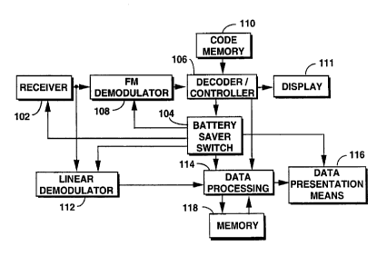
FIG. 1 is an electrical block diagram of a dual mode
communication receiver of the present invention which
overcomes the problems described, and which is compatible
for use on existing paging systems, using existing paging
signaling protocols. The dual mode communication receiver
of the present invention, enables the transmission of data
at very high data bit rates, such as eight kilobits per
second and higher. The dual mode communication receiver of
the present invention is compatible with the existing
paging signaling protocols to provide excellent battery
.,_ WO 94/00923
PCT/US92/05523
7
saving performance characteristics, and to maintain the
receiver sensitivity characteristics of the prior art
' communication receivers using the conventional paging
signaling protocols. The dual mode communication receiver
' S of the present invention is capable of the operation
described above by providing a first receiving means for
receiving and detecting information transmitted in a first
modulation format, such as in the conventional FM modulated
format, and by providing a second receiving means which
is
responsive to the information detected by the first
receiving means in the first modulation format for
receiving and detecting information transmitted in a second
modulation format, such as in one of the linear modulation
formats which enables the high speed transmission of
message information. The transmission format is described
in FIGS. 2A - 2C, and will be described in detail below.
The transmission protocol of FIGS. 2A - 2C enables the
transmission of information which is modulated in a
conventional FM modulation format, and further enables the
transmission of message information which is modulated in
a
linear modulation format to enable high speed data
transmission. Referring to FIG. 1, the information
modulated in either the FM modulation format, or the linear
modulation format, is received by receiver 102. A battery
saving switch 104, under the control of a decoder/
controller 106, supplies power to the receiver 102 to
enable the reception of the transmitted information. The
battery saving switch 104 also couples to an FM demodulator
108 to enable FM modulated information received by receiver
102 to be demodulated. The demodulated information is
provided to the decoder/controller 106. A code memory 110
is provided which couples to the decoder/controller 106,
and which stores address information assigned to the dual
mode communication receiver. When an address is detected
in the demodulated information which corresponds to the
predetermined address information assigned to the
WO 94/00923 PCT/US92/05523 _
g
communication receiver, one of two operations will occur,
which will be described in greater detail below. In the
first instance, the battery saving switch 104, under the
control of the decoder/controller 106 will maintain the
supply of power to the FM demodulator 108 to enable further
demodulation of message information received in the FM
modulation format. The received message information is
temporarily stored in a memory, such as a random access
memory, which is generally located within the
decoder/controller 106. The stored message information is
recalled by the user for display on display 111. The
receiving operating and the decoding of the address
information is well known to one of ordinary skill in the
art.
However, unlike the prior art receivers, power to the
FM demodulator 108 is suspended by battery saver switch
104, under the control of the decoder/controller 106, and
power is then supplied to the linear demodulator 112, to
enable the demodulation of information received in the
second modulation format. The information received in the
second modulation format is received by receiver 102, which
then couples the received information to the linear
demodulator 112. The demodulated message information is
coupled from the output of the linear demodulator 112, to
the input of a data processing unit 114. When the linear
demodulator 112 is enabled, battery saving switch 104 also
supplies power to the data processing unit 114, and to the
data presentation means 116. The decoder/controller 106 is
coupled to the data processing circuit 114, enabling the
data processing circuit 114 to process the message
information received in the second modulation format. The
processed message information is temporarily stored in
memory 118, and can be recalled by the user and displayed
on the presentation means 116.
FIGS. 2A and 2B are timing diagrams describing the
signaling format for the dual mode communication receiver
CA 02139516 1999-06-25
WO 94/00923 PCT/L'S92/p5523
9
of the present invention. As shown in FIG. 2A, when a
message transmission is initiated on the channel, a
preamble 202, modulated in the FM modulation format, is
transmitted on the channel, followed by a plurality o=
message batches 204 - 206. Each of the message bathes 204
- 206 has a predetermined transmission time interval, and
enables the transmission of address and message information
which is modulated in the FM modulation format, or for high
speed data, which is modulated in a linear modulation
format. The modulation of address and message information
in the FM modulation format is well known in the art. The
modulation of data in a linear modulation format, such as
the SEDM modulation format, is described in U.S. Patent No.
4,737,969 to Steel et al, entitled "Spectrally Efficient
Digital Modulation Method and Apparatus" which is assictned
to the assignee of the present invention
All information
transmitted in a given batch is modulated in a common
modulation format. As will be described in further detail
below, one or more batches of information are modulated in
the FM modulation format and can be interleaved with one or
more batches of information which are modulated in a linear
modulation format. Depending upon the channel loading, a
break 208 in the transmission can occur, after which the
preamble 202 is again transmitted to enable the receivers
to re-synchronize with the batch transmission.
FIG. 2B shows in further detail the interleaving of
batches modulated in the FM modulation format with batches
modulated in the linear modulation format. In the
preferred embodiment of the present invention, the preamble
202 is a sequence of alternating one and zero bits which
are modulated using the FM modulation format. The preamble
202 enables the receiver to awake from a battery saving
time interval, recognize that a transmission on the channel
has been initiated, and enables the receiver to obtain bit
synchronization with the transmitted signal. Following the
WO 94/00923 ~ PCT/US92/05523 _
preamble 202 transmission, each batch comprises a
synchronization code word 219, followed by address 210 and
message 212 information, or by high speed data 216. The
synchronization code word 214 is modulated in the
5 modulation format appropriate for the type of data being
transmitted in the batch, and enables synchronization with
the transmitted information. In the example shown. in FIG.
2B, the synchronization code word 214 is modulated in the
FM modulation format, followed by addresses 210 and
10 messages 212 which are also modulated in the FM modulation
format. Each transmission batch is coded using a coded
synchronization code word and allows for the transmission
of a predetermined number of address and/or message
information code words, which, as for example, is sixteen.
As shown, the address 210 of a first receiver and the
associated message 212 are transmitted, followed by the
address 210' of a second receiver and the associated
message 212', and so forth. Message 212' for the second
receiver is not a normal message information code word, but
is a predetermined "batch" pointer, directing the receiver
to the transmission batch in which the high speed message
information directed to the receiver is to be transmitted,
which as shown is in the next transmission batch 218'. As
shown, batch 218' contains the high speed message
information 216 which is modulated in a linear modulation
format. Batch 218' begins with the synchronization code
word 214' which is used to signal the start of the message
information, as will be described below. Following the
transmission of batch 218', additional high speed message
information can be transmitted in additional batches, other
conventionally modulated address and message information
can be transmitted in additional batches, or as shown, the
batch transmission can be terminated until a later time
when additional address and message information is
available for transmission.
WO 94/00923 ~ 9 ~ i ~ PCT/US92/05523
11
FIG. 2C is a timing diagram describing the battery
saver operation for the dual mode communication receiver of
the present invention. Power is initially supplied to the
receiver section, during time interval 220, and to the FM
demodulator, during time interval 222, to enable receiving
the preamble and synchronization code word information
modulated in the FM modulation format. The supply of power
to the linear demodulator is inhibited during time interval
224, thereby conserving power within the receiver. After
having detected the preamble and synchronization code word,
the supply of power to the receiver is maintained during
time interval 220', and to the FM demodulator during time
interval 222', in order to receive any additional address
and message information transmitted in the first
transmission batch. The supply of power to the receiver
section is maintained during time interval 230 since the
next transmission batch includes the high speed data
directed to the receiver. However, the supply of power to
the FM demodulator is suspended during time interval 228,
and power is supplied to the linear demodulator, during
time interval 232. After receiving the high speed data
information during time interval 232, the supply of power
is suspended during time interval 234 to the receiver
section, and during time interval 236 to the linear
demodulator. Power is again supplied to the receiver
section during time interval 238, and to the FM
demodulator, during time interval 240, to again enable
reception of the message information in the next sequence
of message batch transmissions.
In summary, power is regularly supplied to the
receiver and to the FM demodulator to enable reception of
an address and message information using a signaling
protocol which provides battery saving capability to the
receiver. When the message information indicates a high
35~ speed data transmission is forthcoming, the supply of power
to the FM demodulator is suspended, and power is supplied
WO 94/00923 ~ ~ PCT/US92/05523
12
to the linear demodulator to enable the reception of the
high speed data. By supplying power to the linear
demodulator and high speed data storage sections only
during the transmission of high speed data, the receiver
battery life can be greatly extended as compared to
receiving all information in the linear modulation format.
An alternate embodiment of the signaling format for
the dual mode receiver of the present invention is shown in
FIG. 2D. In this embodiment, information is transmitted on
two channels, a first channel 250 which is utilized for the
transmission of low speed message information modulated in
an FM modulation format, and a second channel 252 which is
utilized for the transmission of high speed message
information modulated in a linear modulation format. The
batches of low speed data 204A-206A overlay in time the
batches of high speed data 204B-206B. The dual mode
receiver of the present invention operates on the first
channel receiving message information, which can include
conventional numeric or alphanumeric messages intended for
the dual mode receiver. When long alphanumeric messages or
voice messages are to be transmitted, the message pointer
information is transmitted on the first channel directing
the dual mode receiver to a predetermined message batch to
be transmitted on the second channel. After having
received the pointer information, the dual mode receiver
selects the second channel for receiving the high speed
message information during the predetermined batch
identified by the pointer. After having received the high
speed message, the receiver again selects the ffirst
channel. The alternate embodiment of the present invention
shown in FIG. 2D allows a very efficient method of mixing
conventional paging receivers which receive information
modulated in an FM modulation format, with the dual mode
receivers of the present invention by maintaining all low
speed message transmission on the first channel, and all
high speed message transmission on the second channel.
._ WO 94/00923 PCf/US92/05523
13
This enables the use of conventional signaling formats to
be utilized for the transmission of information in the
batches 204A-206A on the first channel, enabling both
conventional receivers and dual mode receivers to be
readily intermixed.
FIG. 3 is an expanded electrical block diagram which
will be used to describe the receiver operation of the dual
mode communication receiver of the present invention. The
transmitted information signal, modulated in the FM
modulation format, or in a linear modulation format, is
intercepted by the antenna 302 which couples the
information signal to the receiver section 102, and in
particular to the input of the radio frequency (RF)
amplifier 306. The message information is transmitted on
any suitable RF channel, such as those in the high band,
UHF band, and 900 MHz band, The RF amplifier 306 amplifies
the received information signal, such as that of a signal
received on a 930 MHz paging channel frequency, coupling
the amplified information signal 306A to the input of the
first mixer 308. A first oscillator signal 310A, which is
generated in the preferred embodiment of the present
invention by a frequency synthesizer 310, also couples to
the first mixer 308. The first mixer 308 mixes the
amplified information signal 306A and the first oscillator
signal 310A, to provide a first intermediate frequency, or
IF, signal 308A, such as a 45 MHz IF signal, which is
coupled to the input of the first IF filter 312. It will
be appreciated that other IF frequencies can be utilized as
well, especially when other paging channel frequencies are
utilized. The output of the IF filter 312 which is the on-
channel information signal 312A, is coupled to the input of
the second conversion section 314, which will be described
in further detail below. The second conversion section 314
mixes the on-channel information signal 312A to a lower
intermediate frequency, such as at 455 KHz, using a second
oscillator signal 310B, which is also generated by the
WO 94/00923 PCT/US92/05523
14
synthesizer 310. The second conversion section 314
amplifies the resultant intermediate frequency signal, to
provide a second IF signal which is suitable to be coupled
to either the FM demodulator section 108, or to the linear
output section 324.
Receiver section 304 operates in a manner similar to a
conventional FM receiver, however, unlike a conventional FM
receiver, the receiver section 304 of the present invention
also includes an automatic frequency control section 316
which is coupled to the second conversion section 314, and
which appropriately samples the second IF signal to provide
a frequency correction signal 316A which is coupled to the
frequency synthesizer 310 to maintain the receiver tuning
to the assigned channel. The maintenance of receiver
tuning is especially important for the proper reception of
the high speed data information which is transmitted in the
linear modulation format. The use of a frequency
synthesizer to generate the first and second oscillator
frequencies enables the operation selection of the receiver
on multiple operating frequencies, selected such as by code
memory programming. It will be appreciated that other
oscillator circuits, such as fixed frequency oscillator
circuits which can be adjusted by a frequency correction
signal from the automatic frequency control section 316,
can be utilized as well.
An automatic gain control 320 is also coupled to the
second conversion section 314 of the dual mode receiver of
the present invention. The automatic gain control 320
samples the second IF signal, providing a gain correction
signal 320A which is coupled to the RF amplifier 306 to
maintain a predetermined gain for the RF amplifier 306.
The gain correction signal also couples to the second
conversion section 314 to maintain a predetermined gain for
the second conversion section 314. The mainterv~nce of the
gain of the RF amplifier 306 and the second c~w~ersion
section 314 is required for proper reception of the high
WO 94/00923 PCT/US92/05523
speed data information transmitted in the linear modulation
format, and further distinguished the dual mode receiver of
the present invention from a conventional FM receiver.
When the message information is transmitted in the FM
5 modulation format, the second IF signal is coupled to the
FM demodulator section 108, as will be explained in detail
below. The FM demodulator section 108 demodulates the
second IF signal in a manner well known to one of skill in
the art, to provide a recovered data signal 108A which is a
10 stream of binary information corresponding to the received
address and message information transmitted in the FM
modulation format. The recovered data signal 108A couples
to the input of a microcomputer 106, which functions as a
decoder and controller, through a single data input line of
15 input/output port, or I/O port 328. The microcomputer 106
provides complete operational control of the communication
receiver 300, providing such functions as decoding, message
storage and retrieval, display control, and alerting, just
to name a few. The microcomputer 106 is preferably a
single chip microcomputer, such as the MC68HC05
microcomputer manufactured by Motorola, and includes a CPU
340 for operational control. An internal bus 330 connects
each of the operational elements of the microcomputer 106.
I/0 port 328 (shown split in FIG. 3) provides a plurality
of control and data lines providing communications to
microcomputer 106 from external circuits, such as the
battery saver switch 104, audio processor 114, a display
111, and digital storage 368. A timing means, such as
timer 334 is used to generate the timing signals required
for the operation of the communication receiver, such as
for battery saver timing, alert timing and message storage
and display timing. Oscillator 332 provides the clock for
operation of CPU 340, and provides the reference clock for
timer 334. RAM 338 is used to store information utilized
in executing the various firmware routines controlling the
operation of the communication receiver 300, and can also
WO 94/00923 PCT/US92/05523
16
be used to store short messages, such as numeric messages.
ROM 336 contains the firmware routines used to control the
microcomputer 106 operation, including such routines as
required for decoding the recovered data signal 322A,
battery saver control, message storage and retrieval in the
digital storage section 368, and general control of the
pager operation and message presentation. An alert
generator 342 provides an alerting signal 1066 in response
to decoding the FM modulated signalling information. A
code memory 110 (not shown in FIG. 3) couples to
microcomputer 106 through the I/O port 328. The code
memory is preferably an EEPROM (Electrically Erasable
Programmable Read Only Memory) which stores one or more
predetermined addresses to which communication receiver 300
is responsive.
When the FM modulated signaling information is
received, it is decoded by the microcomputer 106,
functioning as a decoder in a manner well known to one
skilled in the art. When the information in the recovered
data signal 322A matches any of the stored predetermined
addresses, the subsequently received information is decoded
to determine if additional information is directed to the
receiver which is modulated in the FM modulation format,
or if the additional information is modulated in the linear
modulation format. When the additional information is
transmitted in the FM modulation format, the recovered
message information is received and stored in the
microcomputer RAM 338, or in the digital storage section
368, as will be explained in further detail below, and an
alerting signal 1066 is generated by alert generator 342.
The alerting signal 1066 is coupled to the audio processing
circuit 344 which drives a transducer 346, delivering an
audible alert. Other forms of sensible alerting, such as a
tactile or vibrating alert, can also be provided to alert
the user as well.
WO 94/00923 . PCT/US92/05523
17
When additional information is to be transmitted in
the linear modulation format, the microcomputer 106 decodes
the pointer information. The microcomputer 106 maintains
the operation of monitoring and decoding information
transmitted in the FM modulation format, until the end of
the current batch, at which time the supply of power is
suspended to the receiver until the next assigned batch, or
until the batch identified by the pointer is reached,
during which high speed data is transmitted. The
microcomputer 106, through I/O port 328 generates a battery
saving control signal 106D which couples to battery saver
switch 104 to suspend the supply of power to the FM
demodulator 108, and to supply power to the linear
demodulator 112, including linear output section 324, the
quadrature demodulator 350, and the digital storage section
368, as will be described in detail below.
The second IF output signal, which now carries the
high speed data information is coupled to the linear output
section 324. The output of the linear output section 324
is coupled to the quadrature detector 350, specifically to
the input of the third mixer 352. A third local oscillator
also couples to the third mixer 352, which is preferably in
the range of frequencies from 35-150 KHz, although it will
be appreciated other frequencies may be utilized as well.
The signal from the linear output section 324 is mixed with
the third local oscillator signal 354, producing a third IF
signal at the output of the third mixer 352, which is
coupled to a third IF amplifier 356. The third IF
amplifier is a low gain amplifier which buffers the output
signal from the input signal. The third output signal is
coupled to an I channel mixer 358 and a Q channel mixer
360. An I/Q oscillator 362 provides quadrature oscillator
signals at the third IF frequency which are mixed with the
third output signals in the I channel mixer 358 and the Q
channel mixer 360, to provide baseband I channel signals
and Q channel signals at the mixer outputs. The baseband I
WO 94/00923 1 PCT/US92/05523
- 18
channel signal is coupled to low pass filter 364, and the
baseband Q channel signal is coupled to low pass filter
366, to provide a pair of baseband audio signals which
represent a stream of information symbol pairs
corresponding to the encoded high speed data information.
The stream of information symbol pairs are coupled to
the digital storage section 368, in particular to the
inputs of an analog to digital (A/D) converter 370. The
A/D converter 370 samples the pair of information symbols
at a rate at least twice the highest frequency component
(in Hz) at the output of 364 and 366. For three kilohertz
voice information encoded on the I and Q channels, the
sampling rate is preferably six kilohertz per I and Q
channel, or twelve kilohertz in total. It will be
appreciated, the data sampling rate indicated is for
example only, and other sampling rates may be used
depending upon the rate at which the message information is
originally encoded.
During the batch during which the high speed data is
transmitted, the microcomputer 106 provides a count
enabling signal 106A which is coupled to the address
counter 372. The A/D converter 370 is also enabled to
allow sampling of the information symbol pairs. The A/D
converter 370 generates high speed sample clock signals
370A which are used to clock the address counter 372 which
in turn sequentially generates addresses for loading the
sampled information symbol pairs into a dual port random
access memory 374 through data lines 370B. The information
symbol pairs which have been loaded at high speed into the
dual port RAM 374 in real time, are processed by the
microcomputer 106 after all high speed data has been
received, thereby producing a significant reduction in the
energy consumed by not requiring the microcomputer 106 to
process the information in real time. The microcomputer
106 accesses the stored information symbol pairs through
data lines 106C and address lines 106B, and in the
21~~~1~
.,~ WO 94/00923 PCT/US92/05523
19
preferred embodiment of the present invention, processes
the information symbol pairs to generate either ASCII
encoded information in the case of alphanumeric data having
been transmitted, or CVSD encoded data in the case voice
data was transmitted. Other data formats, such as a BCD
data format for numeric messages or LPC encoded data format
for voice messages, may be utilized as well. The ASCII
encoded or CVSD encoded data is stored in the dual port RAM
until the information is requested for presentation by the
communication receiver user. The stored ASCII encoded data
is recovered by the user using switches (not shown) to
select and read the stored messages. When the stored ASCII
encoded message is to be read, the user selects the message
to be read and actuates a read switch which enables the
microcomputer 106 to recover the data, and to present the
recovered data 106E to a display 111, such as a liquid
crystal display. When a CVSD encoded message is to be
read, the user selects the message to be read and actuates
the read switch which enables the microcomputer 106 to
recover the data from the dual port RAM, and to present the
recovered data 106E to the audio processor 114 which
functions as a CVSD decoder, converting the digital voice
information into an analog voice signal which is coupled to
a speaker 116 for presentation of the voice message to the
user. The microcomputer 106 can also generate a frequency
selection signal 106H which is coupled to frequency
synthesizer 310 to enable the selection of different
operating frequencies as described above.
FIG. 4 is an electrical block diagram showing details
of the battery saving features of the dual mode
_ communication receiver of the present invention. The
microcomputer 106 controls the battery saving operation of
the communication receiver through battery saver controls
signals 106D coupled to the battery saver switch 104. The
battery saver switch 104 enables power to be selectively
supplied to the receiver section 102 via receiver supply
WO 94/00923 ~ ~ ~ ~ ~ PCT/US92/05523 _
line 104A, to the quadrature detector 350 via quadrature
detector supply line 104B, to the digital storage section
368 via digital storage supply line 104C, to the FM
demodulator section 108 which includes a data limiter 380
5 coupled to an FM demodulator 322 via FM demodulator supply
line 104D, and to the linear output section 324 via linear
output supply line 104E. Elements for selectively
switching the supply of power to the each of the receiver
sections are well known, and include such switching devices
10 as transistor switches and switched current source
references, just to name a few. The microcomputer 106
controls the supply of power to the receiver section 102
which includes such elements as the RF amplifier 306, the
first mixer 308, the frequency synthesizer 310, the IF
15 filter 312, the second mixer 382, the second IF amplifier
384, the automatic gain control section 320, and the
automatic frequency control section 316, and to the FM
demodulator 108 during the transmission of FM modulated
message information. The microcomputer 106 also controls
20 the supply of power to the receiver section, the linear
demodulator and the digital storage during the transmission
of linearly modulated message information. The
microcomputer 326 also controls the supply of power to the
the digital storage section during the processing of the
stored high speed message information, and during the
reading of the stored message. In summary, the battery
saver switch 104 under the control of the microcomputer
106, supplies power only to those circuits which are
currently utilized in the receiving or processing of
information, thereby minimizing the energy consumption of
the battery.
FIGS. 5A and 5B are flow charts describing the
operation of the dual mode communication receiver of the
present invention. Referring to FIG. 5A, when the user
turns power on to the receiver, at step 500, the
microcomputer is initialized, at step 502, enabling the
~I395~6
-. WO 94/00923 PCT/US92/05523
21
battery saving routine. Power is supplied to the receiver,
at step 504, and is also supplied to the FM demodulator
section, at step 506 to begin the preamble search and
acquisition routine. The decoder monitors the information
received on the channel, searching for a preamble signal,
at step 508, or some other signal by which bit
synchronization can be obtained. When a preamble signal,
or other signal is not detected within a predetermined
search window time interval, at step 508, the microcomputer
suspends the supply of power to the receiver and to the FM
demodulator, at step 510, and returns to the battery saving
routine, at step 512, until the next time interval during
which power is again supplied to the receiver and to the FM
demodulator.
When preamble is detected, at step 508, and bit
synchronization is obtained, in a manner well known in the
art, the microcomputer begins the synchronization code word
acquisition routine, at step 514. When the synchronization
code word is not detected within a predetermined period of
time, at step 514, the microcomputer suspends the supply of
power to the receiver and to the FM demodulator, at step
510, and returns to the battery saving routine, at step
512, until the next time interval during which power is
again supplied to the receiver and to the FM demodulator.
When the synchronization code word is detected, at
step 514, corresponding to the batch to which the receiver
is assigned, the microcomputer monitors the received
address and message information, in order that any
addresses and messages directed to the receiver can be
detected, at step 516. When an address is not detected
within the current batch, the microcomputer monitors the
received signal for the synchronization code word, at step
514.
When an address is detected, at step 516, the
microcomputer evaluates the next received code word, at
step 518 to determine if the message information being
WO 94/00923 PCT/US92/05523
22
transmitted is low speed or high speed message information.
When the information transmitted is low speed message
information, the microcomputer recalls information from the
code memory identifying the received address as either a
data address, or a tone only address, at step 520. When
the address is a data address, at step 520, the message
information following the address is stored, at step 522,
and the user is alerted to indicate a message was received.
When the address is identified as a tone only address, at
step 520, the user is alerted to indicate a page was
received. After having received and processed the message,
at steps 522, or 524, the microcomputer returns to the
battery saving routine, suspending the supply of power to
the receiver, at step 510, when no other information is to
be received in the current batch.
When the information received in the first modulation
format indicates a high speed data message is to be
received in the second modulation format, at step 518, the
microcomputer decodes the data pointer, at step 526 of FIG.
5B. When the end of the current batch is detected, the
supply of power to the FM demodulator is suspended, at step
528. The microcomputer determines if the high speed
message information is transmitted on the second channel,
at step 530. When the high speed message is transmitted on
a second channel, the second channel is selected at step
532. When a second channel is not selected at step 530, or
is selected at step 532, power is next supplied to the
linear demodulator during the batch indicated by the
pointer, at step 534, and to the digital storage section,
at step 536. The microcomputer provides an enable signal
to the address counter and to the D/A converter, at step
538, which enables the high speed sampling and storage of
the received data, at step 540. When an end of message
(EOM) character is received, or after a predetermined
number of message bits have been received, at step 540, the
user is alerted that a message has been received, at step
~13951~
.._ WO 94/00923 PCT/US92/05523
23
544. The microcomputer suspends the supply of power to the
linear demodulator, at step 546. Power is maintained to
the digital storage section during Which time the received
high speed data is processed. Upon the completion of the
processing of the high speed message information, the
supply of power is then suspended to the digital storage
section, at step 548. The microcomputer determines~if a
second channel was selected for receiving the high speed
message information at step 550. When a second channel was
selected, at step 550, the microcomputer reselects the
first channel at step 552. When the first channel was
selected at steps 550 or 552, the microcomputer returns to
the normal battery saving routine, at step 512 of FIG. 5A.
A dual mode receiver has been described which is
capable of receiving addresses and messages which are
transmitted in an FM modulation format, and further which
is capable of receiving high speed data messages which are
transmitted in a linear modulation format on either the
same or a different radio frequency channel. The dual mode
receiver includes a battery saving function which
individually controls the supply of power to the FM
demodulator, the linear demodulator, and to the digital
storage section, thereby minimizing the supply of power
being consumed during normal receiver operation in the FM
modulation mode. When high speed message information is
being received, the digital storage section samples and
stores the high speed message information in real time,
after which the stored message information is processed by
the microcomputer decoder to prepare the information for
display.
While specific embodiments of this invention have been
shown and described, further modifications and improvements
will occur to those skilled in the art. All modifications
which retain the basic underlying principles disclosed and
claimed herein are with the scope and spirit of the present
invention.