Note: Descriptions are shown in the official language in which they were submitted.
2139911
TTTT.F;~ OF TE~T~ TNVT~NTTON
Class AB Push-Pull Drive Circuit, Drive Method Therefor And
Class AB Electronic Circuit Using The Same
RAcKGRouNn OF T~T~ TNVT~NTTON
a) Field of the Invention
The present invention relates to a circuit for driving a
load in a class AB push-pull manner, such as a loudspeaker
drive circuit in an acoustic system, a motor drive circuit in
a servo system or an output circuit in an operational amplifi-
er, and a drive method for such a load driving circuit.
b) Description of the Prior Art
There is known such a class AB push-pull drive circuit
as shown in Fig. 23, for example. The illustrated circuit
comprises an NPN transistor Q1o1 and a PNP transistor Q102,
the emitters of which are connected to each other. A positive
supply voltage Vcc is applied to the collector of the transis-
tor Q1o1 while a negative supply voltage Vss is applied to the
collector of the transistor Q102- A constant current source
Q103 is connected between the collector and base of the tran-
sistor Q1o1 while a constant current source Q104 is connected
between the base and collector of the transistor Q102- Two
diodes D1o1 and D102 are further connected in series between
the bases of the transistors Q1o1 and Q102 These diodes D1o1
and D102 are in a forward biased direction relative to the P-N
junction between the base and emitter of the transistors Q1o1
2139911
and Q102- An external voltage Vi is applied to the connecting
point of the diodes D1ol and D102 while the emitters of the
transistors Qlol and Q102 output a drive current io toward a
load in the post-stage (not shown).
The illustrated circuit can make the drive current io
class AB, as shown in Fig. 24. More particularly, if it is as-
sumed that the emitter voltage of the transistors Qlol and
Q102 is Vo, the collector currents in and ip of the transis-
tors QolOl and Q102 will vary relative to Vi - Vo in such a
manner as shown by broken line in Fig. 24. As a result, the
drive current io = in - ip will vary as shown by solid line in
Fig. 24.
Fig. 25 shows another layout of the class AB push-pull
drive circuit. This circuit uses an N-channel FET (Field-
Effect Transistor) Q105 in place of the NPN transistor Qlo1 as
in the prior art shown in Fig. 23 and a P-channel FET Q106 in
place of the PNP transistor Q102 The sources of the FET Q105
and Q106 are co~n~cted to each other. The connected sources
output a drive current io toward a load in the post-stage (not
shown). A positive supply voltage VDD is applied to the drain
of the FET Q105 while a negative supply voltage Vss is applied
to the drain of the FET Q106 A constant current source Q103
is connected between the gate and drain of the FET Q105 while
a constant current source Q104 is connected between the gate
and drain of the FET Q106 Further, the circuit uses an N-
channel FET Q107 in place of the diode Dlol shown in Fig. 23
and a P-channel FET Q108 in place of the diode Q102- The gates
2l3aall
and drains of the FETs Q107 and Q108 are externally short-
circuited to one another, with the sources thereof receiving a
voltage Vi. This circuit can also provide such characteristics
as shown in Fig. 24.
However, such circuits as shown in Figs. 23 and 25
cannot be used if the supply voltages Vcc, VDD or Vss are low.
In other words, the base voltage of the transistor Q1o1 or the
gate voltage of the FET Q105 cannot exceed the positive supply
voltage Vcc or VDD. Actually, the base voltage of the transis-
tor Q1o1 or the gate voltage of the FET Q105 will further be
limited since the transistor Q1o1 or the FET Q105 has a drop
in the voltage between the base and emitter or between the
gate and source. Similarly, the base voltage of the transistor
Q102 or the gate voltage of the FET Q106 cannot be lower than
the negative supply voltage Vss. There is also a drop in the
voltage between the base and emitter of the transistor Q102 or
between the gate and source of the FET Q106- In these prior
arts, since the potential difference between the positive and
negative supply voltages cannot be fully utilized, the ampli-
tude of the output voltage Vo is smaller than a level deter-
mined by the potential differentce. In other words, these
circuits of the prior art cannot be driven by a relatively low
voltage source.
To overcome such problems, there has been proposed such
a class AB push-pull drive circuit as shown in Fig. 26. This
circuit comprises a PNP transistor Q112 and an NPN transistor
Q114, the collectors of which are connected to each other. A
2l3aall
positive supply voltage Vcc is applied to the emitter of the
transistor Q112 while a negative supply voltage Vss is applied
to the emitter of the transistor Q114- The collectors of the
transistors Q112 and Q114 output a drive current io toward a
load in the post-stage, with a voltage being Vo at this point.
If it is assumed that the collector current of the transistor
Q112 is ip and the collector current of the transistor Q114 is
in~ the outputted drive current io becomes ip - in.
The transistors Q112 and Q114 are connected to PNP and
NPN transistors Qlll, Q113, respectively. An e~ternal voltage
Vi is applied to the base of the transistor Qlll and also to
the collector of an NPN transistor Q118 which forms part of a
differential input circuit 101. In addition to the transistor
Q118, the differential input circuit 101 comprises another NPN
transistor Q117 having its emitter connected to that of the
first transistor Q118, a constant current source Qll9 for
supplying a constant current to the emitters of the transis-
tors Q117 and Q118, and constant current sources Q120 and Q121
for supplying constant currents to the collectors of the
transistors Q117 and Q118- The transistor Q118 is connected in
parallel to two diodes Dl11 and D112 which are connected in
series to each other in the forward biased direction relative
to the P-N junction between the base and emitter of the tran-
sistor Q118- The diodes Dll1 and D112 receive a constant
current from a constant current source Q122- Thus, the voltage
between the base and emitter of the transistor Q118 is main-
tained constant. The base of the transistor Q113 is connected
- 213~911
to the collector of the transistor Q117 which is paired with
the transistor Q118-
The base of the transistor Q117 is connected to thecollector of the PNP transistor Q115 and also to the emitter
of the PNP transistor Q116- A positive supply voltage Vcc is
applied to the emitter of the transistor Q115 while a negative
supply voltage Vss is applied to the collector of the transis-
tor Q116- In the circuit of the prior art, therefore, the
voltage between the base and emitter of the transistor Q112 is
transferred between the base and emitter of the transistor
Q116, so that the sum of the voltage between the base and
emitter of the transistor Q114 and the voltage between the
base and emitter of the transistor Q112 is applied to the base
of the transistor Ql17- As described, the base of the transis-
tor Q117 receives a voltage relating to two P-N junctions
between the diodes D111 and D112. The differential input
circuit 101 compares the voltages relating to these diodes
with the voltages between the base and emitter in the transis-
tors Q114 and Q112- Thus, the current io can be driven in
class AB.
Unlike the circuit shown in Fig. 23, the circuit of Fig.
26 can be driven by a relatively low supply voltage since the
amplitude range of the output voltage Vo will not be affected
by the voltage between the base and emitter in the transistors
Q112 and Q114 which relate to the output. However, such a
circuit of the prior art also raises other problems.
First, the circuit of Fig. 26 produces a phase dif-
2l3~
-
ference between signals amplified by two push-pull amplifica-
tion paths, since they provide a large path difference. More
particularly, the circuit of Fig. 26 provides two amplifica-
tion paths, a first path of the base of the transistor Q111
the emitter thereof~ the base of the transistor Q112 ~ the
collector thereof and a second path of the base of the tran-
sistor Q111 ~ the emitter thereof ~ the base of the transistor
Q115 ~ the collector thereof ~ the base of the transistor Q117
the collector thereof~ the base of the transistor Q113 ~ the
emitter thereof ~ the base of a transistor Q114 ~ the collec-
tor thereof. As can be seen from Fig. 26, the difference
between these two signal amplification paths is very large.
Second, the circuit of Fig. 26 includes two closed
negative-feedback loops for class AB drive. These closed
negative-feedback loops tend to oscillate. More particularly,
these two closed negative-feedback loops are a first loop of
the base of the transistor Q111 ~ the emitter thereof ~ the
base of the transistor Q115 ~ the collector thereof ~ the base
of the transistor Q117 ~ the emitter thereof ~ the emitter of
the transistor Q118 ~ the collector thereof ~ the base of the
transistor Q111 and a second loop of the base of the transis-
tor Q113 ~ the emitter thereof ~ the base of the transistor
Q116 ~ the emitter thereof ~ the base of the transistor Q117
the collector thereof ~ the base of the transistor Q113 Both
of these loops tend to oscillate.
2139911
~IJM~Y OF T~ TNV~TTON
It is a first object of the present invention to provide
a class AB push-pull drive circuit and drive method therefor,
which can increase the output amplitude thereof to perform a
class AB drive to a load even if the supply voltage is rela-
tively low. A second object of the present invention is to
provide a class AB push-pull drive circuit and a drive method
therefor, which can provide a reduced difference between push-
pull signal amplification paths so that no phase difference
between signals will be produced, for example, in a high-
frequency region. A third object of the present invention is
to provide a class AB push-pull drive circuit and a drive
method therefor which do not require any closed negative-feed-
back loop for class AB drive and which can thus make the class
AB drive more stable with reduced oscillation. A fourth object
of the present invention is to provide a class AB push-pull
drive circuit and a drive method therefor which can be made
more stable by temperature-compensating the operation.
In a first aspect of the present invention, there is
provided a class AB push-pull drive circuit comprising:
a) first to fourth semiconductor elements each having a
supply electrode, a drive electrode and a control electrode,
the first and second semiconductor elements having a first
polarity and the third and fourth semiconductor elements
having a second polarity, the supply electrodes of the first
to fourth semiconductor elements being connected together, a
current substantially equal to that of each respective supply
2i39~1i
electrode flowing through each of the drive electrodes, the
current flowing in each of the drive electrodes being con-
trolled by the corresponding one of the control electrodes;
b) a first constant voltage circuit for maintaining a
constant voltage between the control electrodes of the first
and third semiconductor elements;
c) a second constant voltage circuit for maintaining a
constant voltage between the control electrodes of the second
and fourth semiconductor elements; and
d) a first output circuit for outputting a class AB
drive current which is generated by inverting and adding the
currents flowing in the drive electrodes of the first and
third semiconductor elements.
In a second aspect of the present invention, there is
provided an class AB push-pull drive circuit comprising:
. a) first to fourth semiconductor elements each having a
supply electrode, a drive electrode and a control electrode,
the first and second semiconductor elements having a first
polarity and the third and fourth semiconductor elements
having a second polarity, the supply electrodes of the first
to fourth semiconductor elements being connected together, a
current substantially equal to that of each respective supply
electrode flowing through each of the drive electrodes, the
current flowing in each of the drive electrodes being con-
trolled by the corresponding one of the control electrodes;
b) a first constant voltage circuit for maintaining a
constant voltage between the control electrodes of the first
2139911
and third semiconductor elements;
c) a second constant voltage circuit for maintaining a
constant voltage between the control electrodes of the second
and fourth semiconductor elements; and
d) a second output circuit for outputting a class AB
drive current which is generated by inverting and adding the
currents flowing in the drive electrodes of the second and
fourth semiconductor elements.
In the first and second aspects, the voltage between the
control electrodes (bases or gates) of the first and third
semiconductor elements is maintained constant by the first
constant voltage circuit while the voltage between the control
electrodes of the second and ~ourth semiconductor elements is
maintained constant by the second constant voltage circuit.
The supply electrodes (emitters or sources) of these semicon-
ductor elements (e.g., bipolar transistors or FETs) are con-
nected together. Therefore, the drive electrode currents
(collector or drain currents) of the semiconductor elements
will increase or decrease in the exponential function manner
(bipolar transistor) or in the quadratic function manner (FET)
relative to the voltage between the control electrodes of the
first and second semiconductor elements or the voltage between
the control electrodes of the third and fourth semiconductor
elements. The drive electrode currents of the first and fourth
semiconductor elements increases or decreases with those of
the second and third semiconductor elements in the differen-
tial relationship. When the first output circuit is used to
2139~11
invert and add the drive electrode currents of the first and
third semiconductor elements or when the second output circuit
is used to invert and add the drive electrode currents of the
second and fourth semiconductor elements, therefore, a class
AB drive current can be provided. At this time, the circuit of
the present invention will not produce any phase difference
between signals in a high-frequency region, since it provides
a reduced difference between signal amplification paths for
class AB drive. The circuit of the present invention does not
require any loop for class AB drive. Thus, the circuit can
operate more stably with less abnormal oscillation.
In a third aspect of the present invention, there is
provided an class AB push-pull drive circuit comprising:
a) first to fourth semiconductor elements each having a
supply electrode, a drive electrode and a control electrode,
the first and second semiconductor elements having a first
polarity and the third and fourth semiconductor elements
having a second polarity, the supply electrodes of the first
to fourth semiconductor elements being connected together, a
current substantially equal to that of each respective supply
electrode flowing through each of the drive electrodes, the
current flowing in each of the drive electrodes being con-
trolled by the corresponding one of the control electrodes;
b) a first constant voltage cirCuit for maintaining a
constant voltage between the control electrodes of the first
and third semiconductor elements;
c) a second constant voltage circuit for maintaining a
2139911
-
constant voltage between the control electrodes of the second
and fourth semiconductor elements;
d) a first output circuit for outputting a class AB
drive current which is generated by inverting and adding the
currents flowing in the drive electrodes of the first and
third semiconductor elements; and
e) a second output circuit for outputting another class
AB drive current which is generated by inverting and adding
the currents flowing in the drive electrodes of the second and
fourth semiconductor elements.
In the third aspect of the present invention, the first
and second output circuits are both provided. Thus, the cir-
cuit can output the class AB drive currents in a differential
manner. More particularly, an electronic class AB circuit for
outputting the class AB drive currents in the differential
manner can be realized since the first class AB drive current
provided by the first and third semiconductor elements is in
the differential relationship with the second class AB drive
current provided by the second and fourth semiconductor ele-
ments.
According to the present invention, the first and second
output circuits are formed by current mirror circuits. First
and third current mirror circuits, respectively corresponding
to the first and third semiconductor elements, are connected
to each other such that the output currents from these semi-
conductor elements are inverted and added to generate a class
AB drive current. Similarly, second and fourth current mirror
2139~11
,
circuits, respectively corresponding to the second and fourth
class AB drive currents, are connected to each other such that
the output currents from these semiconductor elements are
inverted and added to generate a class AB drive current.
Therefore, a load in the post-stage can be driven through an
increased current by setting an increased mirror ratio in the
current mirror circuits. The connections between the first and
third current mirror circuits and between the second and
fourth current mirror circuits can be realized by push-pull
connecting the output transistors of the current mirror cir-
cuits.
The first to fourth semiconductor elements may be bipo-
lar transistors or FETs. With bipolar transistors, the charac-
teristics of the collector currents are of exponential func-
tion relative to inputs. The characteristics of the FET drain
currents are of quadratic function relative to inputs.
Each of the first and second constant voltage circuits
includes a first or second temperature characteristic compen-
sating means. The temperature-to-voltage characteristics of
the first and third semiconductor elements is compensated by
the first temperature characteristic compensating means while
the temperature-to-voltage characteristics of the second and
fourth semiconductor elements are compensated by the second
temperature characteristic compensating means. Such an ar-
rangement can realize a class AB push-pull drive circuit which
is stable relative to temperature independently of the temper-
ature-to-voltage characteristics of each of the semiconductor
213~
elements between the control and supply electrodes.
Each of the temperature characteristic compensating
means may be formed by two temperature compensating elements.
More particularly, four temperature compensating elements are
provided each having its temperature-to-voltage characteris-
tics substantially equal to those of the corresponding one of
the first to fourth semiconductor elements. The first tempera-
ture compensating element having its temperature-to-voltage
characteristics substantially equal to those of the first
semiconductor element is forwardly connected in series to the
third temperature compensating element having its temperature-
to-voltage characteristics substantially equal to those of the
third semiconductor element. The second temperature compensat-
ing element having its temperature-to-voltage characteristics
substantially equal to those of the second semiconductor
element is forwardly connected in series to the fourth temper-
ature compensating element having its temperature-to-voltage
characteristics substantially equal to those of the fourth
semiconductor element. Further, the series connection between
the first and third temperature compensating elements is
forwardly connected in parallel to the first and third semi-
conductor elements while the series connection between the
second and fourth temperature compensating elements is for-
wardly connected in parallel to the second and fourth semicon-
ductor elements. In such a manner, the temperature compensa-
tion can preferably be realized.
The temperature compensating elements may be provided by
2l3sall
P-N junctions. More particularly, P-N junctions of the same
design as those between the control and supply electrodes of
the first to fourth semiconductor elements may be used as
first to fourth temperature compensating elements. These P-N
junctions receive a constant current from the first constant
current source.
Where the first to fourth semiconductor elements are
formed by bipolar transistors, the P-N junctions are also
formed by bipolar transistors of the same design as those of
the first to fourth semiconductor elements. By short-circuit-
ing between the collector and base of each of the bipolar
transistors, it can provide a P-N j unction between the base
and emitter. Alternatively, the P-N junction between the base
and emitter of a bipolar transistor having the same design as
those of the first to fourth semiconductor elements and driven
by a biasing bipolar transistor may be used when a circuit for
driving the base of the bipolar transistor is used and the
base of the biasing transistor is driven by the first constant
current source. Alternatively, the P-N junction between the
base and emitter of a bipolar transistor having the same
design as those of the first to fourth semiconductor elements
and driven by a biasing bipolar transistor may be used when a
circuit for driving the base of the bipolar transistor is used
and the base of the biasing transistor is driven by the second
constant current source. If the first to fourth semiconductor
elements are formed by FETs, the temperature compensation
similar to that of the bipolar transistors can be realized by
14
2139~11
short-circuiting between the gate and drain of each of the
FETs and using the first constant current source. At this
time, the second constant current source may be used to drive
the gate of the FET. When the class AB push-pull drive circuit
is formed into an integrated circuit, the temperature compen-
sation may be further improved by utilizing the bipolar tran-
sistors or FETs since they can easily realize components of
the same characteristics as those of the first to fourth
semiconductor elements.
The present invention further provides three different
methods for driving the class AB push-pull drive circuit which
are classified depending on in which manner a differential
input voltage is applied to the first to fourth semiconductor
elements. More particularly, there are a first method, in
which the differential input voltage is applied directly to
the first and second semiconductor elements; a second method,
in which the differential input voltage is applied directly to
the third and fourth semiconductor elements; and a third
method, in which the differential input voltage is applied to
all the semiconductor elements indirectly (i.e., through parts
of the first and second constant voltage circuits). All the
methods can drive the class AB push-pull drive circuit very
well.
The first class AB electronic circuit of the present
invention includes a differential input circuit for generating
a differential current on application of the differential
input voltage, the differential current being then supplied to
2139911
the first and second constant voltage circuits. The first and
second constant voltage circuits are responsive to the differ-
ential current to execute the aforementioned function of
holding the constant voltage. The second class AB electronic
circuit includes first and second differential input circuits
which are driven by the same constant current. Each of the
first and second differential input circuits is responsive to
the differential input voltage for outputting first or second
differential current. The first constant voltage circuit
directly or indirectly receives the first and second differen-
tial currents to execute the constant voltage holding function
while the second constant voltage circuit uses the interme-
diate value between the positive and negative supply voltages
as a reference to execute the constant voltage holding func-
tion. Thus, the load in the post-stage can be class AB driven
even when a difference between the positive and negative
supply voltages is relatively small or even if the supply
voltage is relatively low.
RRT~F n~ RTpTToN OF THF. l)RAWTNG.C;
Fig. 1 is a circuit diagram showing the primary parts of
a first embodiment according to the present invention.
Fig. 2 is a circuit diagram showing the primary parts of
a second embodiment according to the present invention.
Fig. 3 is a circuit diagram showing the primary parts of
a third embodiment according to the present invention.
Fig. 4 is a view showing the characteristics of collec-
2139~11
tor current where IeOl=IeO2
Fig. 5 is a view showing the characteristics of collec-
tor current where IeOl~IeO2
Fig. 6 is a circuit diagram showing the primary parts of
a fourth embodiment according to the present invention.
Fig. 7 is a circuit diagram showing the primary parts of
a fifth embodiment according to the present invention.
Fig. 8 is a circuit diagram showing the primary parts of
a sixth embodiment according to the present invention.
Fig. 9 is a view showing the characteristics of drain
current.
Figs. lOA - lOE are views showing various constant vol-
tage circuits usable in the first to third embodiments.
Figs. llA - llC are views showing various constant vol-
tage circuits usable in the first to third embodiments.
Fig. 12 is a circuit diagram of a class AB differential
output circuit formed by using the circuit relating to the
second embodiment of the present invention.
Fig. 13 is a circuit diagram of a class AB differential
output circuit formed by using the circuit relating to the
fifth embodiment of the present invention.
Fig. 14 is a circuit diagram showing an operational
amplifier formed by using the circuit relating to the second
embodiment of the present invention.
Fig. 15 is a circuit diagram showing an operational
amplifier formed by using the circuit relating to the fifth
embodiment of the present invention.
213~911
-
Fig. 16 is a circuit diagram showing an operational
amplifier formed by using the circuit relating to the second
embodiment of the present invention.
Fig. 17 is a circuit diagram showing an operational
amplifier formed by using the circuit relating to the second
embodiment of the present invention.
Fig. 18 is a circuit diagram showing an operational
amplifier formed by using the circuit relating to the fifth
embodiment of the present invention.
Fig. 19 is a circuit diagram showing another output
circuit.
Fig. 20 is a circuit diagram showing still another
output circuit.
Fig. 21 is a circuit diagram showing a further output
circuit.
Fig. 22 is a circuit diagram showing a further output
circuit.
Fig. 23 is a circuit diagram showing a first circuit
constructed in accordance with the prior art.
Fig. 24 is a view illustrating a class AB push-pull
drive circuit constructed according to the prior art.
Fig. 25 is a circuit diagram showing a second circuit
constructed in accordance with the prior art.
Fig. 26 is a circuit diagram showing a third circuit
constructed in accordance with the prior art.
18
2139911
n~TATT~T~n nT~cRTpTToN OF T~ p~T~T~T~RRT~n T~MRonTMT~T~
Some preferred embodiments of the present invention will
now be described with reference to the drawings.
a) Arrangements of First to Third Embodiments
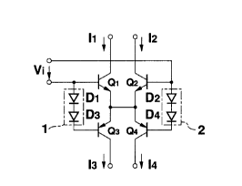
Fig. 1 shows the primary parts of a class AB push-pull
drive circuit constructed according to the first embodiment of
the present invention. The first embodiment includes NPN
transistors Q1, Q2 and PNP transistors Q3, Q4, the emitters of
which are connected together. A constant voltage circuit 1
consisting of two diodes D1 and D2 is connected between the
bases of the transistors Q1 and Q3 while a constant voltage
circuit 2 consisting of two diodes D2 and D4 is connected
between the bases of the transistors Q2 and Q4. Each of the
diodes D1 to D4 is forwardly connected to the P-N junction
between the base and emitter of the corresponding one of the
transistors Q1 to Q4. A differential input voltage V1 is
applied across the bases of the transistors Q1 and Q2.
Fig. 2 shows a class AB push-pull drive circuit con-
structed according to the second embodiment of the present
invention. The second embodiment is different from the first
embodiment in that the differential input voltage Vi is ap-
plied across the connecting point between the diodes D1 and D3
and the connecting point between the diodes D2 and D4.
Fig. 3 shows the primary parts of a class AB push-pull
drive circuit constructed according to the third embodiment of
the present invention. In the third embodiment, the differen-
tial input voltage Vi is applied across the bases of the
2139911
transistors Q3 and Q4.
In any of these embodiments, the emitters of two NPN
transistors Ql and Q2 and the emitters of two PNP transistors
Q3 and Q4 are connected together. Further, the differential
input voltage Vi is applied to across the bases of the tran-
sistors Ql and Q2 and across the bases of the transistors Q3
and Q4 directly or through parts of the voltage circuits 1 and
2. As will be described later, the constant voltage circuits 1
and 2 receive constant currents to maintain the voltages
between the bases of the transistors Ql and Q3 and between the
bases of the transistors Q2 and Q4 constant. According to the
first to third embodiments, the class AB push-pull drive
circuit which can be driven by a relatively low drive voltage
is realized to increase the output amplitude. The ciucuit
also provides a reduced difference in signal paths which
results in an improved symmetry and is stable in temperature
without the need of any loop for class AB operation.
b) Driving Mechanism of First to Third Embodiments
The driving mechanism of the first to third embodiments
will be described below:
The relationship between the base-emitter voltage Vbe
and the emitter outflow current Ien Of an NPN transistor, the
relationship between the emitter-base voltage Veb and the
emitter inflow current Iep of a PNP transistor and the rela-
tionship between the voltage Vd and the current Id of a P-N
junction diode can be generally represented by the following
formulas:
213~911
Vbe = VT-ln (Ien/Isn)
Veb = VT ln (Iep/Isp)
Vd = VT ln (Id/Isd) (1)
VT = k-T/q (2)
where ISn~ Isp and ISd are reverse~direction saturation cur-
rents determined by the manufacturing process of the transis-
tors or diodes, and the size of the transistors or diodes
used; k is Boltzmann's constant (= 1.38066 x 10⁻²³ (J/K)); and
q is a unit charge = 1.60216 x 10⁻¹⁹ (C). Therefore, the
voltage VT depending on the absolute temperature T (K) is
about 26 (mV) at room temperature and the temperature coeffi-
cients of the above voltages Vbe, Veb and Vd become equal to
about -2 mV/~C.
To illustrate the operation of each of the embodiments
in symplified manner, it is now assumed that the transistors
Ql and Q2 are of the same size; the transistors Q3 and Q4 are
of the same size; and the constant voltage circuits 1 and 2
are of the same size. It is also assumed that the voltage
drops of the constant voltage circuits 1 and 2 are equal to
each other and also equal to Es. Further, the emitter currents
and base-emitter voltages of the transistors Ql to Q4 are
respectively represented by Iel to Ie4 and Vbel to Vbe4 and
the emitter current when the differential input voltage Vi is
equal to zero is represented by IeO. A formula (3) obt~;ne~
when the aforementioned formula (1) is applied to the transis-
tors Ql and Q2, a formula (4) obtained when the aforementioned
formula (1) is applied to the transistors Q3 and Q4, a formula
2139911
(5) obtained when the aforementioned formula (1) is applied to
the transistors Q1 and Q3 and a formula (6) obtained when the
aforementioned formula (1) is applied to the transistors Q1
and Q3, when the differential input voltage Vi is equal to
zero, are as follows:
Vi = Vbel - Vbe2
= VT-ln (Iel/ISn) - VT-ln (Ie2/Isn)
= VT-ln (Iel/Ie2) (3)
Vi = (Es + Vbe4) - (Es + Vbe3)
= VT-ln (Ie4/Isp) - VT-ln (Ie3/ISp)
= vT-ln (Ie4/Ie3)
Es = Vbel + Vbe3
= VT-ln (Iel/Isn) + VT-ln (Ie3/ISp)
= VT-ln {(Iel-Ie3)/(Isn~Isp)}
Es = Vbel + Vbe3
= VT-ln (IeO/Isn) + VT ln (Ieo/ISp)
= VT-ln {(IeO-IeO)/(Isn~Isp)} (6)
Since the emitters of the transistors Ql to Q4 are
connected together, the following formula is established:
Ie1 + Ie2 = Ie3 + Ie4 (7)
A formula (8) obtained by comparing the formulas (3) and
(4), a formula (9) obtained by the comparison result of the
formulas (5) and (6) and by the formula (8), and a formula
(10) obtained by comparing the formulas (7) and (8), are as
follows:
Ie1/Ie2 = Ie4/Ie3 (8)
Iel~Ie3 = Ie2~Ie4 = IeO2 (9)
21~9~11
Iel = Ie4 ~ Ie2 = Ie3 ( 10 )
By modifying the formulas (3), (4), (9) and (10), the
following formulas (11) to (13) are obtained:
Vi = VT-ln (Iel~Ie4/Ieo2)
= VT-ln (Ieo2/Ie2-Ie3)
= 2-vT-ln (Iel/IeO)
= 2-vT-ln (Ie4/IeO)
= 2-vT-ln (IeO/Ie2)
= 2-vT-ln (IeO/Ie3) (11)
Iel = Ie4 = Ieo-exp (Vi/VT) (12)
Ie2 = Ie3 = Ieo-exp (-Vi/VT) (13)
Thus, the emitter current Iel of the transistor Ql
becomes equal to the emitter current Ie4 Of the transistor Q4
while the emitter current Ie2 Of the transistor Q2 becomes
equal to the emitter current Ie3 Of the transistor Q3. The
emitter currents Iel, Ie4 and Ie2, Ie3 exponentially increase
or decrease relative to the differential input voltage Vi, the
former Iel, Ie4 and latter Ie2, Ie3 being in differential
relationship to each other. In addition, as is well known, the
emitter current of a transistor is substantially equal to the
collector current of the same. Therefore, the characteristics
of the collector currents Il to I4 of the respective transis-
tors Ql to Q4 in each of the aforementioned embodiments rela-
tive to the differential input voltage Vi are as shown in Fig.
4. As will be apparent therefrom, differential currents bet-
ween the currents Il and I3 and between the currents I2 and I4
become class AB currents.
213~
When an output circuit for inverting and adding the
currents is used with the circuits shown in Figs. l to 3, a
load supplied with the currents through the output circuit can
be driven as in class AB. Even where a plurality of signal
amplification paths are generated, a difference between the
paths can be eliminated. Therefore, any phase difference
between signals in the high-frequency region can be prevented.
Further, it is difficult any abnormal oscillation to be creat-
ed, since the circuit does not require a loop for class AB
drive. In addition, the class AB push-pull drive circuit will
be more stable in temperature by compensating the temperature
characteristics of the P-N junction between the base and
emitter of each of the transistors Ql to Q4 through the diodes
Dl to D4, since the constant voltage circuits l and 2 are de-
fined by the diodes Dl to D4.
Fig. 5 shows the characteristics of the collector cur-
rents Il to I4 when the emitter current Ieol of the transistor
Ql is not equal to the emitter current Ieo2 Of the transistor
Q2 when the differential input voltage Vi is equal to zero.
Such characteristics as shown in Fig. 5 can be represented by
the following formulas:
/ leol+leo2 eXp(vi/vr)
r eo1 t Ieo 2~ ex p ( -Vi / Vr )
leol exp(-vi/vT)-Ieoz (15)
leol ~ exp ( vi / Vr)+Ieo2
24
2139911
eol ~ leoz . ex p ( - vi / VT) (16)
eOI t leo2 exp ( vi/vr)
/ Ieo~ ~ exp ( Vi /Vr) + Ieoz
~i Ieol exp ~ -vi/vr) ~leo2
As will be apparent from these graph and formulas, the
class AB current can be similarly obtained.
c) Arrangements of Fourth to Sixth Embodiments
Fig. 6 shows the primary parts of a class AB push-pull
drive circuit constructed according to the fourth embodiment
of the present invention. The fourth embodiment uses N-channel
FETs Q5 and Q6 in place of the NPN transistors Q1 and Q2 in
the first embodiment and also utilizes P-channel FETs Q7 and
Q8 in place of the PNP transistors Q3 and Q4. The sources of
the FETs Q5 to Q8 are connected together. The constant voltage
circuit 1 is formed by N-channel FET Q9 and P-channel FET Q11
the gates and drains of which are connected together. The
constant voltage circuit 2 iS formed by N-channel FET Qlo and
P-channel FET Q12, the gates and drains of which are connected
together. Each of the FETs Q9 to Q12 iS connected in the
forward biased direction relative to the gate-source voltage
of the corresponding one of the FETs Q5 to Q8. A differential
input voltage Vi is applied to between the gates of the FETs
Q5 and Q6-
Fig. 7 shows a class AB push-pull drive circuit con-
structed according to the fifth embodiment of the present
2139~11
invention. The fifth embodiment is different from the fourth
embodiment in that the differential input voltage Vi is ap-
plied across the connecting point of the FETs Qg and Q11 and
the connecting point of the FETs Q1o and Q12
Fig. 8 shows a class AB push-pull drive circuit con-
structed according to the sixth embodiment of the present
invention. In the sixth embodiment, the differential input
voltage Vi is applied across the gate of the FET Q7 and the
gate of the FET Q8
In any of the fourth to sixth embodiments, the sources
of the two N-channel FETs Qs, Q6 and sources of the two P-
channel FETs Q7, Q8 are connected together. Further, the
differential input voltage Vi is applied directly across the
gates of the FETs Qs and Q6, or directly across the gates of
the FETs Q7 and Q8, or through parts of the voltage circuits 1
and 2. As in the first to third embodiments, the constant
voltage circuits 1 and 2 receive a constant current to main-
tain the voltage between the base of the FET Qs and the gate
of the FET Q7 or between the gate of the FET Q6 and the gate
of the FET Q8 constant. According to the fourth to sixth
embodiments, thus, the class AB push-pull drive circuit which
can be driven by a relatively low voltage is realized to
increase the output amplitude. The circuit also reduces the
difference between signal path lengths, which results in
improved symmetry. Further, the class AB push-pull drive
circuit can be more stable in temperature. The circuit can be
implemented without the need of any loop for class AB drive.
26
2139~11
d) Driving Mechanism of Fourth to Sixth Embodiments
The driving mechanism of the fourth to sixth embodiment
will now be described.
The drain currents Idn and Ipn of N-channel and P-chan-
nel FETs are generally represented by the following formulas:
Idn = ~q~n (coxwl/2Ll)(vgsl-vtl)2
= KnVg12 (18)
pn = q~p (Coxw2/2L2)(vgs2-vt2)2
= KpVg22 ( 19 )
where q = unit charge;
~n and~p = mobility of electron and hole;
COX = thickness of gate oxide film;
W1 and W2 = gate width;
L1 and L2 = gate length;
Vgsl and Vgs2 = gate-source voltage;
Vt1 and Vt2 = threshold voltage;
Kn = ~n (coxwl/2Ll);
Kp = ~p (coxw2/2L2);
Vg1 = Vgsl - Vtl;
Vg2 = Vgs2 - Vt2;
Subscript 1 = N channel; and
Subscript 2 = P channel.
For illustration, it is assumed that the FETs Qs and Q6
are of the same size; that the FETs Q7 and Q8 are of the same
size; and that the voltage drops of the constant voltage cir-
cuits 1 and 2 are equal to each other. It is also assumed that
the absolute value of Kn is equal to that of Kp (K = Kn =
2139911
-Kp). When the drain currents of the FETs Qs to Q8 are respec-
tively represented by Is to I8 while the gate-source voltages
thereof are respectively represented by Vgs to Vgg, the drain
currents Is to I8 when the differential input voltage Vi is
inputted can be represented by the following formulas:
Is = Kn (Vgl - Vg2)2 = KVi2 (20)
I6 = ~Kn (Vg1 - Vg2)2 = -KVi2 (21)
I7 = Kp (Vg4 - Vg3)2
= Kp (Vg1 - Vg2)2 = -KVi2 (22)
I8 = -Kp (Vg4 - Vg3)2
= -Kp (Vgl - Vg2)2 = KVi2 (23)
Therefore, formulas (24) and (25) are obtained from the
formulas (20), (23) and (21), (22), respectively.
Is = I8 (24)
I6 = I7 (25)
As will be apparent from the formulas (24) and (25), the
drain current Is of the FET Qs is equal to the drain current
I8 Of the FET Q8 while the drain current I6 Of the FET Q6 is
equal to the drain current I7 of the FET Q7. As can also be
seen from the formulas (20) to (24), the drain current pairs
(Is, I6) and (I7, Ig) will increase or decrease relative to
the differential input voltage Vi in the quadratic function
manner, these pairs being in differential relationship to each
other. Thus, the relationship of the drain currents Is - I8 in
the FETs Qs - Q8 Of the fourth to sixth embodiments with the
differential input voltage Vi will be as shown in Fig. 9. As
will be apparent from such characteristics, the differences
2139911
between the currents Is and I7 and between the currents I6 and
I8 become class AB currents.
When the circuits shown in Figs. 6 - 8 are used with an
output circuit for inverting an adding the currents, a load
supplied with the currents through the output circuit can be
driven in class AB. Even where a plurality of signal amplifi-
cation paths are generated, a difference between the paths can
be eliminated. Therefore, any phase difference between signals
in the high-frequency region can be prevented. Further, it is
difficult for any abnormal oscillation to be created since the
circuit does not require a loop for class AB drive. In addi-
tion, the class AB push-pull drive circuit will be more tem-
perature stable due to compensation of the temperature charac-
teristics between the gate and source of each of the FETs Qs -
Q8 through the N-channel FETs Qg, Q1o and P-channel FETs Q11,
Q12 the gates and sources of which are connected together,
since the constant voltage circuit 1 and 2 are defined by the
FETs Qg - Q12
e) Forms of Constant Voltage Circuit
Figs. lOA to lOE show five forms of the constant voltage
circuit 1 or 2 which are usable in the first to third embodi-
ments of the present invention.
In a constant voltage circuit shown in Fig. lOA, the
diode D1 or D2 is connected in series with the diode D3 or D4.
These diodes are further connected in series with two resis-
tors I and to two constant current sources (Q13 or Q14) and
(Q15 or Q16)- The constant current sources (Q13 or Q14) and
2139911
(Q15 or Q16) provide constant currents to the diodes (Dl or
D2) and (D3 or D4) to maintain a constant voltage drop Es. The
resistors I serve to regulate the voltage drop Es.
In a constant voltage circuit shown in Fig. lOB, the
diode (Dl or D2) is formed by a transistor (Q17 or Q18) which
is short-circuited between the collector and base thereof. The
diode (D3 or D4) is formed by a transistor (Ql9 or Q20) which
is short-circuited between the base and collector thereof.
In a constant voltage circuit of Fig. lOC, the transis-
tor (Q17 or Q18) is of NPN type, rather than PNP type as in
Fig. lOB. Similarly, the transistor (Ql9 or Q20) is of PNP
type, rather than NPN type.
In a constant voltage circuit of Fig. lOD, the collector
and base of the transistor (Q17 or Q18) are shunted by an NPN
transistor (Q21 or Q22) while the collector and base of the
transistor (Ql9 or Q20) are shunted by a PNP transistor (Q23
or Q24)
In a constant voltage circuit shown in Fig. lOE, two
resistors I are connected between the base of a transistor
(Q25 or Q26) and the base of a transistor (Q27 or Q28) The
connecting point between these resistors I serves as a voltage
application point. The bases of the transistors (Q25 or Q26)
and (Q27 or Q28) receive constant currents from two constant
current sources (Q29 or Q30) and (Q31 or Q32), respectively.
The emitter of the transistor (Q2s or Q26) receives a constant
current from a constant current source (Q33 or Q34) while the
emitter of the transistor (Q27 or Q28) receives a constant
2139311
current from a constant current source (Q3s or Q36) A voltage
Es appearing between the emitters of the transistors (Q25 or
Q26) and (Q27 or Q28) is constant. In other words, this em-
bodiment provides the diode (Dl or D2) defined by the transis-
tor (Q25 or Q26) and the upper resistor I and the diode (D3 or
D4) formed by the transistor (Q27 or Q28) and the lower resis-
tor I.
Figs. llA - llc show three different forms of the con-
stant voltage circuit 1 or 2 which are usable in the fourth to
sixth embodiments of the present invention.
In a constant voltage circuit shown in Fig.llA, an N-
channel FET (Qg or Q1o) is connected in series with a P-chan-
nel FET (Qll or Q12) These FETs are further connected in
series with two resistors I and two constant current sources
(Q13 or Q14) and (Q15 or Q16) The constant current sources
(Q13 or Q14) and (Q15 or Q16) provide constant currents to the
FETs (Qg or Qlo) and (Qll or Q12) to maintain the illustrated
constant voltage drop Es. The resistors I serve to regulate
the voltage drop Es.
A constant voltage circuit shown in Fig. llB utilizes a
P-channel FET (Q37 or Q38) in place of the N-channel FET (Qg
or Q1o) and an N-channel FET (Q3g or Q40) in place of the P-
channel FET (Qll or Q12)
In a constant voltage circuit of Fig. llC, two resistors
are connected between the gates of FETs (Q41 or Q42) and
(Q43 or Q44), the connecting point between these resistors
being a voltage application point. The gates of the FETs (Q41
21399'11
or Q42) and (Q43 or Q44) receive constant currents from two
constant current sources (Q29 or Q30) and (Q31 or Q32)- The
source of the FET (Q41 or Q42) is supplied with a constant
current from a constant current source (Q33 or Q34) while the
source of the FET (Q43 or Q44) is supplied with a constant
current from a constant current source (Q3s or Q36)- There-
fore, a constant voltage Es will appear between the sources of
the FETs (Q41 or Q42) and (Q43 or Q44)-
f) Applied Circuit Examples
Fig. 12 shows a class A8 output circuit modified from
the second embodiment of the present invention, the circuit
having a differential output. Although the illustrated circuit
includes the same constant voltage circuits 1 and 2 as in Fig.
lOB, they may be replaced by those of Fig. lOA and lOC - lOE.
The collectors of the transistors Q1 - Q4 are respec-
tively connected to the collectors and bases of transistors
Q4s ~ Q48 which function as input diodes of current mirror
circuits 3 - 6. The collector of an output transistor Q4g in
the current mirror circuit 3 is connected to the collector of
an output transistor Qs1 in the current mirror circuit 5.
Similarly, the collector of an output transistor Q50 in the
current mirror circuit 4 is connected to the collector of an
output transistor Qs2 in the current mirror circuit 6. Thus,
the collectors of the transistors (Q49, Q51) and (Q50, Q52)
will provide two different class AB drive currents which are
in a differential relationship with each other. Such a differ-
ential relationship will be apparent from Figs. 4 and 5.
32
2139911
Fig. 13 shows a class AB output circuit having a differ-
ential output, which is modified from the fifth embodiment of
the present invention. In this circuit, the PNP and NPN tran-
sistors (Q1 ~ Q4), (Q17 ~ Q20) and (Q45 - Q52) are replaced by
P- and N-channel FETs (Q5 ~ Q8), (Q37 - Q40) and (Q53 ~ Q60)
Although the class AB output circuit uses the same constant
voltage circuits as shown in Fig. llB, they may be replaced by
those of Figs. llA or llC.
Fig. 14 shows an operational amplifier formed by the
second embodiment of the present invention, which uses the
same constant voltage circuits 1 and 2 as shown in Fig. lOB.
The operational amplifier comprises a differential input
circuit 7 formed by two NPN transistors Q61 and Q62 A differ-
ential input voltage Vi is externally applied to the bases of
the transistors Q61 and Q62 A current mirror circuit 8
provides, to the emitters of the transistors Q61 and Q62, a
constant current which is determined by the supply voltages
Vcc, Vss, a resistance R and its own mirror ratio. The emit-
ters of the transistors Q17 and Q18 in the constant voltage
circuits 1 and 2 receive currents corresponding to the collec-
tor currents of the transistors Q62 and Q61 through current
mirror circuits 9 and 10, respectively. Further, the emitter
current of the transistor Ql9 is maintained at the same amount
as that of the transistor Q20 by a current mirror circuit 11.
The collectors of the transistors Q2 and Q4 are connected to
current mirror circuits 12 and 13, respectively. The output
transistors Q63 and Q64 Of the current mirror circuits 12 and
33
213~
13 function as output transistors in the illustrated opera-
tional amplifier. The collectors of the transistors Q17 and
Ql9 are respectively connected to those of the transistors Q63
and Q64 through a capacitor Cl.
In such an arrangement, the operational amplifier may
have the aforementioned advantages with a class AB output.
Fig. 15 shows another operational amplifier formed by
the fifth embodiment of the present invention. This operation-
al amplifier uses the same constant voltage circuits as shown
in Fig. llB and P- or N-channel FETs Q6s ~ Q68 in place of the
PNP or NPN transistors Q61 or Q64 as in Fig. 14.
Fig. 16 shows a further operational amplifier construct-
ed according to the second embodiment of the present inven-
tion. Unlike the circuit of Fig. 14, the operational amplifier
shown in Fig. 16 utilizes the same constant voltage circuits 1
and 2 as shown in Fig. lOD. Each of current mirror circuits 14
and 15 defining an output circuit includes a PNP transistor
Q6g or Q70 having its collector which is driven by Vss or Vcc.
In such an arrangement, therefore, the mirror ratio in the
current mirror circuits 14 and 15 can be increased. As a
result, a load can be driven by a relatively large current.
Fig. 17 shows a still further operational amplifier
constructed according to the second embodiment of the present
invention, in which the same constant voltage circuits 1 and 2
as in Fig. lOE are used.
The emitter of a transistor Q2s receives a positive
constant current through current mirror circuits 16 and 17,
34
2139911
the constant current being determined by the supply voltages
Vcc, Vss, resistance ~ and mirror ratios. More particularly,
the aforementioned constant current source Q33 is formed by
the resistor R and current mirror circuits 16, 17. Similarly,
the emitter of a transistor Q27 receives a constant current
from a constant current source Q3s which is formed by the
resistor R and current mirror circuit 17. The base of the
transistor Q2s receives a constant current from a constant
current source Q2g which is defined by the resistor R and
current mirror circuits 17, 18 while the base of the transis-
tor Q27 receives a constant current from a constant current
source Q31 which is formed by the resistor R and current
mirror circuits 19, 20.
The emitter of a transistor Q26 defining the constant
voltage circuit 2 receives a constant current from a constant
current source Q34 which is defined by the resistor R and
current mirror circuits 16, 17 while the emitter of a transis-
tor Q28 defining the constant voltage circuit 2 receives a
constant current from a constant current source Q36 which is
defined by the resistor R and current mirror circuits 17. The
bases of the transistors Q26, Q28 externally receive an inter-
mediate voltage between the positive supply voltage Vcc and
the negative supply voltage Vss, that is, (Vcc + Vss)/2.
The differential input voltage Vi is applied across the
bases of the transistors Q6s and Q66 and also across the bases
of the transistors Q67 and Q68. The transistors Q6s and Q66
define a differential input circuit, with their emitters
2139911
receiving a constant current from the current mirror circuit
17. The collectors of the transistors Q6s and Q66 are respec-
tively connected to transistors Q6g and Q70 each of which is
short-circuited between the base and collector thereof. The
transistor Q6g serves as an input transistor in a current
mirror circuit 21 while the transistor Q70 serves as an input
transistor in a current mirror circuit 18. The collector of an
output transistor Q71 in the current mirror circuit 21 is
connected to the bases of transistors Q72 and Q73 in the
current mirror circuit 20 while the collector of the transis-
tor Q73 is connected to the bases of transistors Q2s and Q27
The collector of an output transistor Q74 in the current
mirror circuit 18 is also connected to the bases of the tran-
sistors Q25 and Q27
The transistors Q67 and Q68 similarly define a differen-
.tial input circuit. The emitters of the transistors Q67 and
Q68 receive a constant current from a current mirror circuit
19. The collector of the transistor Q67 is connected to an
input transistor Q7s in a current mirror circuit 22 while the
collector of the transistor Q68 is connected to an input
transistor Q72 in the current mirror circuit 20. An output
transistor Q76 Of the current mirror circuit 22 is connected
to the base of an output transistor Q74 of the current mirror
circuit 18 such that the output transistor Q76 is exactly
symmetrical with the transistor Q71
When, in such a manner, the constant voltage circuit 2
is actuated by each reference voltage (Vcc + Vss)/2, the base
36
2139~11
of the transistor Q2s is driven by the output of the differen-
tial input circuit formed by the transistors Q6s and Q66 and
the base of the transistor Q2s is driven by the output of the
differential input circuit defined by the transistors Q67 and
Q68, and a load connected to the post-stage can be driven in
the class AB drive manner even if a difference between the
supply voltages Vcc and Vss is relatively low, for example,
equal to about 1.5 Volts.
Fig. 18 shows a further operational amplifier construct-
ed according to the fifth embodiment of the present invention.
The operational amplifier uses the same constant voltage
circuits 1 and 2 as in Fig. llE and FETs (Q5 ~ Q8), (Q41 ~
Q44) and (Q77 ~ Q88) in place of the bipolar transistors (Ql ~
Q4), (Q25 ~ Q28) and (Q65 ~ Q76) which are shown in Fig. 17.
g) Supplement
As described, the output circuits in the first to third
embodiments are current mirror circuits formed using bipolar
transistors while the output circuits in the fourth to sixth
embodiments are current mirror circuits defined by FETs.
However, the present invention is not limited to such output
circuits.
As shown in Fig. 19, for example, the bases of output
transistors Q8g and Qgo may be driven by the collectors of the
transistors Q2 and Q4. In such a case, the collector currents
of the transistor Q2 and Q4 are inversely amplified and thus
obtained currents flow through the collectors of the transis-
tors Q8g and Qgo. Namely, the current output characteristics
37
2l3sall
within the inversely amplifying characteristics of the bipolar
transistors Q8g and Qgo are obtained. Alternatively, the cur-
rent mirror circuits 12 and 13 at the output stage may be
comprised of FETs as shown in Fig. 20. In this figure, the
transistors Q91 and Q92 which constitute the current mirror
circuit 12 are PMOSFETs, respectively, while the transistors
Qg3 and Qg4 which constitute the current mirror circuit 13 are
NMOSFETs, respectively. The aforementioned advantages are also
obtained by this circuit structure.
As shown in Fig. 21, for example, the bases of output
transistors Qgs and Q96 may be driven by the drains of the
FETs Q6 and Q8. In such a case, the drain currents of the FETs
Q6 and Q8 are inversely amplified and thus obtAine~ currents
flow through the collectors of the transistors Qgs and Q96
Namely, the current output characteristics within the inverse-
ly amplifying characteristics of the transistors Qgs and Q96
are obtained. Alternatively, as shown in Fig. 22, the current
mirror circuits 12 and 13 at the output stage may be comprised
of bipolar transistors. In this figure, the transistors Qg7
and Q98 which constitute the current mirror circuit 12 are PNP
transistors, respectively, while the transistors Qgg and Q1oo
which constitute the current mirror circuit 13 are NPN tran-
sistors, respectively. The aforementioned advantages are also
obtained by this circuit structure.
h) Advantages
As described, the class AB push-pull drive circuit of
the present invention comprises first to fourth semiconductor
38
2139911
elements having their supply electrodes connected together,
the voltages between the control electrodes of the first and
third semiconductor elements and between the control elec-
trodes of the second and fourth semiconductor elements being
maintained constant. Therefore, a current obtained by invert-
ing and adding the drive electrode currents of the first and
third semiconductor elements or the drive electrode currents
of the second and fourth semiconductor elements becomes a
class AB drive current. The class AB push-pull drive circuit
does not require any loop for class AB drive. Therefore, an
abnormal oscillation will not be produced and a difference
between signal amplification paths can be reduced to make the
circuit more stable. Where each of the first and second con-
stant voltage circuits for holding the constant voltages is
formed by two P-N junctions connected in series with each
other, the temperature characteristics of each of the semicon-
ductor elements can be compensated to stabilize the class AB
push-pull drive circuit with respect to temperature.
Where an electronic circuit such as operational amplifi-
er is formed by a class AB push-pull drive circuit constructed
according to the present invention, current mirror circuits
are used as output circuits. If the mirror ratio is increased,
a load can be driven by a relatively large current in the
class AB drive manner. When the class AB push-pull drive
circuit is so constructed that the second constant voltage
circuit is actuated by an intermediate voltage between the
positive and negative supply voltages as a reference and that
39
2t39911
the first constant voltage circuit is actuated by a differen-
tial input voltage, the post-stage load can be driven in the
class AB drive manner even if a difference between the posi-
tive and negative voltages is relatively low. In other words,
the class AB push-pull drive circuit can be actuated by a
relatively low voltage.