Note: Descriptions are shown in the official language in which they were submitted.
2I39972
DATA CONVERTING DEVICE
Background of the Invention
The present invention relates to a data converting device
for converting input data such as image data or voice data
according to a users request, and more particularly, to a
data converting device for converting data by employing a
multitude of look-up-tables (LUTs) composed of converting data
corresponding to input data.
In the conventional image output apparatus such as a
color printer or facsimile, when image quality is compensated
l5 for brightness, contrast or tilt employing an LUT, LUTs for
compensating each image quality, which are defined by each
compensation mode, have to be stored in discrete ROMs. For
example, when image quality is compensated by three kinds of
compensation modes, three memory devices are needed for
storing three kinds of LUTs.
FIG. 1 is a block diagram showing a data converting
device using LUT in a conventional color printer. First,
second and third ROMs 12, 14 and 16 are memory devices for
storing LUT data for each converting mode. First, second and
third latches 11, 13 and 15 latch the data input to each latch
so as to output the latched data in accordance with a clock
signal. First and second delays 17 and 18 generate a delayed
clock signal for controlling latches 13 and 15 connected to
the output of each ROM.
When input data 101 is input periodically, first latch 11
1
~1~99'~2
latches input data 101 and output the latched data to first
ROM 12 in accordance with clock signal 110. Output data 102
from first latch 11 becomes a lower address of first ROM 12. A
first condition data 107 determines converting level with
respect to the LUT stored in first ROM 12 and becomes an upper
address of first ROM 12. That is, an address for accessing
first ROM 12 consists of a lower address, i.e., output data
102 of first latch 11, and an upper address, i.e., first
condition data 107. Data 103 output from first ROM 12 is data
which is converted by a first LUT according to input data 101
and first condition data 107.
A first delay 17 delays clock signal 110 by a time period
equal to the time delay between the input and output of first
ROM 12 and generates the delayed clock signal 111 to be output
IS to second latch 13. Second latch 13 connected to an output of
first ROM 12 outputs to second ROM 14 the latched data 103
output from first ROM 12 according to the delayed clock signal
111. An address for accessing second ROM 14 consists of a
lower address, i.e., output data 104 of second latch 13, and
an upper address, i.e., second condition data 108. Data 105
output from second ROM 14 is data which is secondly converted
,by a second LUT according to second condition data 108 and
data 104 which is firstly converted by the first LUT.
Second delay 18, third latch 15 and third ROM 16 operate
as described above. Then, the data 113 thirdly converted by a
third LUT of third ROM 16 according to the secondly converted
data 106 and third condition data 109 is finally output.
The relationship between first, second and third
2
condition data 107, 108 and 109 and the LUTs stored in first,
second and third ROMs 12, 14 and 16 can be explained as
follows. First condition data 107 determines a conversion
level with respect to the converting mode of the first LUT and
generally given by a user. For example, if input data is 8-bit
image data, the first LUT stored in first ROM 12 is for
controlling a brightness level of image, and the brightness
level can be controlled by four steps, the number of input
data is 2$ - 256, that is, from 0 to 255, the first LUT
consists of 256 byte (256 x 8 bits) data by steps, and the
first condition data consists of 2-bit data for representing
the four steps.
FIG. 2A to FIG. 2C illustrate the data structure of the
ROM employed for the conventional data converting device. Each
LUT can compensate data in accordance with four steps in each
converting mode, and the memory capacity of each ROM is
divided into four regions, and converting data in accordance
with each step is stored in each divided region.
As described above, the conventional data converting
device connects in series ROMs which are as many as the number
of the required LUTs and sequentially reads LUT data stored in
each ROM, to thereby perform a data conversion. In general, a
plurality of devices included in the peripheral control
circuitry of ROMs can be miniaturized into a single chip such
as ASIC, but ROMs for storing LUTs are not included in ASIC,
considering modification of ROM contents, if necessary.
Accordingly, device miniaturization is restricted and the
volume of the required hardware and manufacturing cost are
3
~~399'~2
increased since memory devices are needed in accordance with
the number of LUTs according to the kinds of converting mode.
Summary of the Invention
Accordingly, it is an object of the present invention to
provide a data converting device for storing a multitude of
LUTs in a single memory device to convert data.
To accomplish the above object, there is provided a data
converting device for generating, with reference to two or
more LUTs sequentially, a converted output data corresponding
to input data and converting level selected by each LUT, the
data converting device comprising:
a single memory device for storing two or more LUTs
corresponding to the number of data converting modes by block
units, each block including a plurality of sub-LUTs
corresponding to the number of converting levels defined in
each corresponding converting mode; and
an address generator for generating an address for
accessing the memory device by an input data, the data
selected among the output data read from the memory device and
the data for selecting converting level in each converting
mode, the address being generated repeatedly as many times as
correspond to the number of LUTs stored in the memory device.
Brief Description of the Drawings
The above objects and other advantages of the present
invention will become more apparent by describing in detail a
preferred embodiment thereof with reference to the attached
4
~~99~~
drawings in which:
FIG.1 is a block diagram showing the constitution of the
conventional data converting device;
FIG.2A to FIG.2C are data structure diagrams of the ROMs
shown in FIG.1;
FIG.3 is a data structure diagram of a ROM applied to the
present invention;
FIG.4 is a block diagram of a data converting device of
the present invention;
FIG S is a detailed block diagram of the data converting
device shown in FIG.4; and
FIG.6A to FIG.6I are t~.ming diagrams for illustrating the
operation of the data converting device shown in FIG S.
Detailed Description of the Invention
FIG. 3 is a data structure diagram of a ROM applied to
the present invention.
The entire memory capacity of a memory device is divided
into blocks corresponding to the number of LUTs required for
the kinds of converting mode, and a memory capacity of each
divided block is divided into sub-blocks corresponding to the
number of conversion levels of the corresponding LUT.
Converting data is stored in the divided blocks and sub-blocks
according to the corresponding converting mode and conversion
level .
An embodiment of the present invention governs the case
that the input data is image data consisted of eight bits,
each LUT is defined by converting mode (for example,
5
2139972
brightness, contrast, etc.) for controlling image quality, and
the image quality can be controlled by four conversion levels
in each converting mode.
In applying the present invention, if the number of bits
of input data, the kinds of converting mode and the number of
conversion levels are different from those of the embodiment
of the present invention, the memory capacity of the blocks
and the sub-blocks of a memory device can be divided
appropriately. In addition, if the memory capacity occupied by
each LUT is different, the memory blocks for each LUT can be
divided into equal capacities or can be variably divided for
an efficient use of memory capacity. For the latter case, a
problem in data accessing caused by a variable constitution of
memory capacity has to be~considered.
In addition, LUT data stored in a memory device includes
various converting data required for apparatus to which the
present invention can be applied, for example, audio or
temperature compensation data as well as image compensation
data.
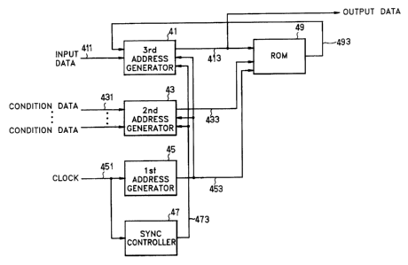
FIG.4 is a block diagram of a data converting device of
the present invention. The data converting device comprises a
ROM 49 for storing a plurality of LUTs in the form as shown in
FIG.3, a first address generator 45 far generating a first
address 453 for sequentially selecting a LUT according to a
converting mode, a second address generator 43 for generating
a second address 433 for selecting a sub-block in the LUT
selected by first address 453 according to a conversion level,
a third address generator 41 for generating a third address
6
CA 02139972 2004-09-30
413 for selecting converting data in the sub-block selected by
first and second addresses 453 and 433, and a sync controller
47 for generating a sync signal 473 for synchronizing first,
second and third addresses 453, 433 and 413 input to ROM 49.
A clock signal 451 is a pulse signal whose period equals
the time interval between input of single input data 411 and
output of the data finally converted by all LUTs stored in ROM
49. Clock signal 451 is synchronized with input data 411 and
input to first address generator 45 and sync controller 47 to
thereby synchronize addresses 453, 433 and 413 for accessing
ROM 49.
First address generator 45 receives clock signal 451 and
generates first address 453 for sequentially selecting the
desired LUT stored in ROM 49. Second address generator 43
generates, according to condition data 431 for determining a
conversion level defined for each LUT, second address 433 for
selecting a sub-block within the LI1T selected by first address
453. Third address generator 41 receives input data 41.1 and
feedback output data 493 and generates third address 413 for
selecting converting data within the selected sub-block. In
other words, input data 411 is generated as third address 413
when data is converted by the first LUT, and the feedback
output data 493 is generated as third address 413 for other
cases. Accordingly, an address for accessing the data of ROM
49 has the order of first, second and third addresses 453, 433
and 413.
FIG. 5 is a detailed block diagram of the data converting
device shown in FIG.4. This embodiment is for the case where
7
three LUTs are stored in ROM 59.
A first address generator 51 comprises a counter 551 for
generating four pulses during one cycle of the input clock
signal 561. The generated signal 550 is output to ROM 59, a
second MUX 531 and a decoder 515.
A second address generator 53 comprises a second MUX 531
having a three-to-one multiplexer for selecting and outputting
one among three types of condition data 541, 542 and 543
according to pulse signal 550 input from counter 551 and a
second latch 532 for latching data 545 output from second MUX
531 and outputting the latched data to ROM 59 according to
sync signal 570.
A third address generator 51 comprises a decoder 515 for
generating the signal 525 for controlling first MUX 511
according to pulse signal 550 input from counter 551, a first
MUX 511 made up of a two-to-one multiplexer where input data
521 and the feedback output data 590 are input for selecting
and outputting one of the input signals 521 and 590 according
to control signal 525 generated from decoder 515, and a first
latch 513 for latching data 523 output from first MUX 511 and
outputting the latched data to ROM 59 according to sync signal
570.
A sync controller 57 comprises first, second and third
delays 571, 572 and 573 for outputting clock signal 561 which
is delayed by a delayed time determined by the data access
time of ROM 59, and an OR gate 575 for performing a logical OR
operation on clock signal 561 and the delayed signals 582, 583
and 584 and thereby generating sync signal 570. The generated
8
sync signal 570 is input to second latch 532 of second address
generator 53 and first latch 513 of third address generator
51.
FIG. 6A to FIG. 6I illustrate the operational timing of
the data converting device shown in FIG.5. Operation of the
device will be explained according to a time sequence and with
reference to the reference numerals of FIG. 5.
FIG. 6A illustrates a waveform of clock signal 561, 6B
illustrates a waveform of input data signal 521, 6C
illustrates a waveform of sync signal 570, 6D illustrates a
waveform of first address signal 550 output from counter 551,
6E illustrates a wavefortn of third address signal 510 output
from first latch 513, 6F illustrates a waveform of second
address signal 530 output from second latch 532, 6G
illustrates a waveform of output signal 582 of first delay
571, 6H illustrates a waveform of output signal 583 of second
delay 572, and 6I illustrates a waveform of output signal 584
of third delay 573.
Sync signal 570 is generated by performing a logical OR
operation on clock signal 561 and the first, second and third
delay signals 582, 583 and 584 which are delayed by a
,predetermined time with respect to clock signal 561. Four
pulses are generated during one cycle of input data signal 521
and are employed for synchronization with addresses input to
ROM 5 9 .
Operation during a first cycle of sync signal 570 can be
explained as follows. Counter 551 outputs first address signal
550 for accessing the first LUT of ROM 59 according to the
9
'~1 ~9~72
clock signal. Second MUX 531 selects first condition data 541
with respect to a conversion level of the first LUT and
outputs the selected data to second latch 532. The latched
data is output as second address signal 530 for accessing ROM
59. Decoder 515 generates a control signal that makes first
MUX 511 select input data 521, and first MUX 511 selects input
data 521 according to the control signal of decoder 515 and
outputs the result to first latch 513, and the latched data is
output as third address signal for accessing ROM 59.
Accordingly, data of the first LUT of ROM 59 is accessed by
the first, second and third address signals 550, 530 and 510,
and the input data is converted by the first LUT and the
first-converted data is fed back and is input to first MUX
511.
Operation during a second cycle of sync signal 570 can be
explained as follows. Counter 551 outputs first address signal
550 for accessing the second LUT of ROM 59 according to the
clock signal. Second MUX 531 selects second condition data 541
with respect to a conversion level of the second LUT and
outputs the selected data to second latch 532. The latched
data is output as second address signal 530 for accessing ROM
,59. Decoder 515 generates a control signal that makes first
MUX 511 select the feedback first-converted data 590, and
first MUX 511 selects the feedback first-converted data 590
according to the control signal of decoder 515 and outputs the
result to first latch 513, and the latched data is output as
third address signal for accessing ROM 59. Accordingly, data
of the second LUT of ROM 59 is accessed by the first, second
2139972
and third address signals 550, 530 and 510, and the feedback
first-converted data is converted by the second LUT and the
second-converted data is fed back and is input to first MUX
511.
Operation during a third cycle of sync signal is the same
as that during the second cycle of the sync signal. Data of a
third LUT of ROM 59 is accessed by first, second and third
address signals 550, 530 and 510, and the feedback second-
converting data is converted by the third LUT and the third-
converted data is fed back and is input to first MUX 511.
During a fourth cycle of the sync signal, first MUX 511
selects the feedback third- converted data 590 and outputs the
selected data to first latch 513. The latched data is output
as finally converted data 510.
According to the present invention, input data is
sequentially converted by all LUTs during one clock cycle, to
thereby generate final output data. Accordingly, when the
number of LUTs for data conversion is increased, output data
is fed back so as to convert data through all LUTs. Therefore,
clock cycle is increased in proportion to the delay time of
ROM. However, such a problem can be solved by reducing the
,access time of the ROM.
As described above, a plurality of LUTs are stored in a
single memory device and a data converting device adopting the
same is provided, so that the data converting device can be
miniaturized by reducing the bulk of the memory device.
11