Note: Descriptions are shown in the official language in which they were submitted.
2140083
Dual-Wavelength Source of High-Repetition Rate,
Tran form-Limited Optical Pul~es
Field of the Invention
This invention relates to a method and apparatus for
producing an optical pulse train. More particularly, this
invention relates to a method and apparatus for producing
optical pulses that are nearly transform-limited which have a
sech-like shape.
Backqround
Numerous methods are known for generating optical pulse
trains at a high-repetition rate in which the pulses are
nearly transform-limited and have a sech-like shape. Such
optical pulses are important, for example, in soliton
transmission systems.
For example, M. Nakazawa, S. Suzuki, Y. Kimura, Opt.
Lett. 15, 715 (1990) disclose optical pulse sources that
employ gain-switched, output-filtered, distributed feedback
(DFB) lasers. However, these lasers suffer from extreme chirp
and excessive timing jitter. Mode-locked semiconductor lasers
using external cavities have also been employed as optical
pulse sources and are disclosed, for example, in the following
references: G. Eisenstein, R. S. Tucker, U. Koren an S.
Korotky, IEEE J. Ouantum Electronics 22, 142 (1986); J. E.
Bowers, P. A. Morton, A. Mar and S. W. Corzine, IEEE J.
Ouantum Electronics, 25, 1426 (1989); R. S. Tucker et al.,
Electron. Lett. 25, 621 (1989); M. C. Wu et al., APpl. Ph~s.
Lett. 57, 759 (1990); and P. B. Hansen et al., IEEE Phot.
2140083
Technol. Lett. 4, 215 (1992). These sources tend to be
difficult to align, have low output power, and are generally
expensive to implement in a practical manner.
Other known sources of optical pulses having the above-
mentioned characteristics include harmonically mode-locked,
modulator-driven, fiber ring lasers. These sources, which
require servo-control of the ring length, also tend to be
expensive and suffer from modulator bias drift. An example of
such a source is disclosed in G. T. Harvey and L. F.
Mollenauer, Opt. Lett. 18, 107 (1993). Other sources, such as
disclosed in M. Suzuki, H. Tanaka, N. Edagawa, K. Utaka, Y.
Matsushima, J. Liqhtwave Technol. 11, 468 (1993), employ an
intensity modulator to carve the pulses from a cw source.
However, these sources also tend to suffer from modulator bias
drift. Finally, some sources employ dual-frequency laser
signals which undergo a nonlinear transformation into the
desired pulse trains. However, for repetition rates less than
20 GMZ, these sources typically require that the pulse-forming
fiber have an impractically long length. An example of such
a source is disclosed in P. V. Mamyshev, S. V. Chernikiov and
E. M. Dianov, IEEE J. Ouantum Electron. QE-27 (2347 (1991).
It is, therefore, an object of this invention to provide
a simple and relatively inexpensive method and apparatus for
generating high quality pulse trains at a high repetition rate
while at the same time avoiding the above-enumerated
deficiencies.
21~0083
Summary
This object is achieved by a method and apparatus in
which
a cw optical signal is phase modulated by an external phase
modulator. The central optical frequencies (i.e., the carrier
frequency and at least one pair of sidebands) of the phase
modulated signal are then removed from the signal. Each of
the remaining side-bands that have not been removed
independently form an optical pulse train of the desired
transform-limited pulses. Accordingly, this example of the
invention forms a dual-wavelength source of high quality
pulses that can form, for example, adjacent channels in a
wavelength-division-multiplexed (WDM) communication system.
In another example of this invention, the initial cw
optical signal is phase modulated as above. At least one of
the Stokes or anti-Stokes components of the modulated optical
signal is then selected. This selected component defines at
least one optical pulse train composed of the desired high
quality pulses.
This invention avoids the deficiencies of known pulse
sources discussed above. For example, this invention requires
no modulator bias setting since only the phase is directly
modulated, not the intensity. Accordingly, the problem of
modulator drift is eliminated.
Brief Description of the Drawinqs
FIG. 1 shows a block diagram of one example of an optical
source for generating high quality optical pulses in
accordance with this invention.
~ 2140083
FIG. 2(a) shows a graph of the external phase modulation
of an optical cw signal as a function of time; FIG. 2(b) shows
a graph of the instantaneous frequency deviation of the phase
modulated cw signal; FIG. 2(c) and 2(d), respectively, show
the anti-Stokes and Stokes spectral components of the phase
modulated cw signal which each form an optical pulse train in
accordance with this invention.
FIG. 3(a) shows an example of the spectral components of
the phase modulated cw signal as a function of the frequency
deviation relative to the unmodulated cw signal; FIGS. 3(b)
and 3(c) show, respectively, the anti-Stokes and Stokes
components of the signal after passing through the optical
filters.
- FIGS. 4(a) and 4(b) show the pulse trains corresponding
to the spectral components shown in FIGS. 3(a) and 3(b),
respectively; FIG. 4(c) shops the pulse train of FIG. 4(b) on
a logarithmic scale.
FIG. 5 shows an expanded view of one of the pulses seen
in FIG. 4(c).
FIG. 6 shows an example of the calculated ratio T/l,
where ~ is the pulse width (FWHM) (solid curve) and the energy
contained in both the Stokes and anti-Stokes pulse trains
(dashed curve), both as a function of the phase modulation
amplitude A.
FIG. 7(a) shows an example of the low-frequency spectral
components for a phase modulation frequency equal to 10 GHz;
FIG. 7(b) is an oscilloscope trace of the 10 GHz pulse train
corresponding to the spectrum of FIG. 7(a).
21~0083
Detailed DescriPtion
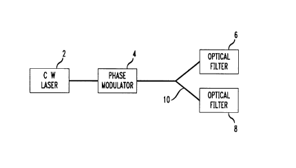
FIG. 1 shows a block diagram of an optical source for
generating high q~ality optical pulses at a high repetition
rate in accordance with this invention. A cw laser 2 is
optically coupled to a phase modulator 4. The phase modulator
4 imparts phase modulation to the cw signal from the laser 2.
The phase modulator 4 is in turn optically coupled to two
optical filters 6 and 8 so that a portion of the signal from
the phase modulator 4 is directed to each of the filters 6 and
8. The optical coupling between the phase modulator 4 and the
optical filters 6 and 8 may be accomplished, for example, with
a Y-branch coupler 10.
The principles upon which the optical source of this
invention operates are as follows. The cw signal from the
laser 2 is phase modulated by the modulator 4 so that its
instantaneous phase is modulated in a periodic manner. While
the periodicity may be chosen as desired, for illustrative
purposes the periodicity will be assumed to be sinusoidal.
Accordingly, the instantaneous phase of the modulated signal
is:
~(t) = Asin(nt) + ~0 (1)
where Q is the modulation frequency and A is the modulation
amplitude. As a result of the modulation, the instantaneous
optical frequency of the modulated signal, ~(t), also changes
with time. The optical frequency deviation is defined as:
214008~
~ (t) _ ~(t) - ~
where ~ is the initial frequency of the cw signal.
Therefore:
8~(t) = a~ = AncOs ( n t) (2)
FIG. l(a) shows the phase modulation of the cw signal
produced by the modulator 4 as a function of time while FIG.
l(b) shows the frequency deviation ~(t) as a function of
time. As FIG. 1 indicates, the signal frequency chirp is
zero (i.e., a(~(t))/at=O) at those times (i.e., t= Txn/2,
where n= O, +- 1, +- 2... , and T= 2~/Q), when the carrier
frequency deviation
¦ ~(t)¦ reaches its maximum value. Those frequency regions
for which the frequency deviation reach a maxima are
indicated by the horizontal dashed lines in FIG. l(b).
These regions define the extreme anti-Stokes (i.e., the
uppermost line) and Stokes (i.e., the lowermost lines)
spectral components of the phase modulated cw signal.
In accordance with this invention, the optical filters
6 and 8 are configured to select, respectively, the extreme
Stokes and anti-Stokes spectral components of the phase
modulated cw signal. Each of these components define a
pulse train that forms the desired high quality, high
repetition-rate pulses. The two pulse trains selected by
the optical filters 6 and 8 are shown in FIGS. 2(c) and
2(d). Thus, as FIGS. 2(c) and 2(d) illustrate, nearly
2190083
transform-limited (i.e., chirp-free) pulses can be obtained
at the corresponding wavelength at a repetition rate R = l/T
determined by the phase modulation frequency.
An important advantage achieved by this invention is
that the generation of the pulse train is independent of the
constant phase bias ~0 (see equations 1 and 2). Thus, this
optical pulse source is insensitive to any drift of the
phase bias which is inherent in most known practical
modulators.
Additional features of this invention will be
illustrated with the use of numerical simulations. FIGS.
3-5 show simulated pulses and pulse trains when the cw laser
signal is phase modulated in accordance with Eq. (1) with
the phase modulation A equal to 1.5~. In particular, FIG.
2(a) shows the spectrum as a function of the frequency
deviation ~(t) (where ~(t) = 0 is the frequency of the
unmodulated cw signal) after the cw signal has undergone
phase modulation but before it has been filtered by the
filters 6 and 8. FIGS. 3(b) and 3(c) show, respectively,
the anti-Stokes and Stokes components of the signal after it
passes through the optical filters 6 and 8. As a comparison
of FIG. 3(a) with FIGS. 3(b) and 3(c) reveals, in this
example the filters 6 and 8 remove the carrier frequency and
the pair of sidebands-nearest to the carrier frequency.
However, the actual number of sidebands removed from the
modulated signal is designer-selectable and depends on the
particular application for which the pulses are to be
employed.
2140083
FIGS. 4(a) and (b) show the pulse trains corresponding
to the spectral components shown in FIGS. 3(a) and (b),
respectively. FIG. 4(c) shows the pulse train of FIG. 4(b)
on a logarithmic scale normalized to the input cw signal
intensity Io~ FIG. 5 shows an expanded view of one of the
pulses seen in FIG. 3(c). As this Figure illustrates, the
shape of the pulses generated by this invention is between
sech2 and Gaussian. In view of this fact, it is not
surprising that the time-bandwidth product is 0.39.
FIG. 6 (solid curve) shows the calculated ratio T/~,
where ~ is the pulse width (FWHM) as a function of the phase
modulation amplitude A. As the curve indicates, the pulse
width decreases as the phase modulation amplitude A
increases. In particular, the ratio T/~ increases from 4.3
to 8.1 as A increases from ~ to 7~.
FIG. 6 also shows (dashed curve) the energy contained
in both the Stokes and anti-Stokes pulse trains (expressed
as a percentage of the input cw signal energy) as a function
of the phase modulation amplitude A. The energy in the
pulse trains varies from 90% to 45~ as the modulation
amplitude A increases from ~ to 7~. It should be noted that
the peak intensity of the generated pulses is 1.7 times
higher than the input cw signal intensity (see FIGS. 4-5).
The spectral sep~ration between the Stokes and anti-
Stokes pulse trains increases with the phase modulation
amplitude A, since the mean frequencies of the two pulse
trains correspond closely to the extrema of the
instantaneous optical frequency created by the phase
--~ 2140083
modulation. Consequently, the difference between the mean,
or carrier frequencies of the pulse trains can be estimated
from Eq.(2):
~ ~ 8~(nt=0) - ~(nt=~) = 2An (3)
A more accurate expression for the difference between the
carrier frequencies of the pulse trains as obtained from
numerical simulations shows that:
~ ~ 1.924(A - 0.9) n (4)
Eq. 4 provides a very good approximation of ~ for a
modulation amplitude A equal to ~ - 7~.
The following numerical example will further illustrate
the features of this invention. If the phase modulator 4
imparts a phase modulation to the cw signal of 10 GHz with
an amplitude A equal to 1.9~, two high-quality 10 GHz trains
with 19 psec pulses are generated. The spectral separation
between the trains is ~/(2~) = 97 GHz. (The corresponding
separation in the wavelength domain ~ is 0.78 nm at ~ =
1550 nm). In this example, the pulse trains contain 77% of
the input cw laser energy. A source of optical pulses such
as set forth in this example could be advantageously
employed in a WDM long-distance soliton transmission system.
In one particular embodiment of the invention, a
single-frequency cw semiconductor laser is employed which
produces a signal at ~ = 1560 nm. The signal is phase
- ' 2140083
modulated by a sinusoidally driven LiNbO3 phase modulator.
The modulation frequency is tunable over a range between 2.5
- 15 GHz. A phase modulation amplitude A approximately
equal to 1.5~ is obtained by applying 32 dBm of rf power to
the modulator. The low-frequency components of the
phase-modulated signal can be selected by using a low-pass
fiber grating filter such as disclosed, for example, in V.
Mizrahi, J. E. Sipe, "Optical Properties of Photosensitive
Fiber Phase Grating", IEEE J. Liqhtwave Technolo~y, 1993.
FIG. 6(a) shows the resulting low-frequency spectrum when
the modulation frequency is equal to 10 GHz. FIG. 6(b)
shows an oscilloscope trace of the 10 GHz pulse train
corresponding to the spectrum of FIG. 6(a). The pulse width
is 21 psec (obtained after deconvolution of the detection
system response of 12 psec), which is in good agreement with
numerical calculations. Similar results can be obtained at
repetition rates of 2.5 -12.6 GHz.
In an alternative example of the invention, the optical
filters 6 and 8 may be replaced by a single filter that
suppresses the central region of the spectrum (i.e., the
carrier signal and possibly one or more pairs of the nearest
side-bands). In this case, of course, further spectral
selection is required to separate the two pulse trains from
one another. This ar~angement is advantageous because pulse
formation and control of the carrier frequency can be
accomplished with a single filter element.