Note: Descriptions are shown in the official language in which they were submitted.
;a~4~99
60557-4762
A DETECTOR PLATE FOR USE IN IMAGING SYSTEMS
Fleld Of The Invention
Thls inventlon relates generally to radlatlon
lmaglng systems and ln partlcular to an lmproved detector
plate for use ln such systems.
Backqround Of The Inventlon
Conventlonal radlatlon lmaglng systems may utlllze
photoconductlve materlals to absorb lncident radlatlon
representatlve of an ob~ect. Unlted States patent 4,176,275
dlscloses a dlgltal x-ray lmaglng system ln whlch a
radlatlon source ls posltioned to dlrect a radlatlon image
of an ob~ect onto the upper surface of a detector plate.
The detector plate lncludes a sultable photoconductlve
materlal that absorbs the radlatlon and produces electron-
hole palrs (flrst charge carrlers) whlch may be separated
from each other by an electrlc fleld applled across the
photoconductor, creatlng a latent lmage of the ob~ect at the
surface of the photoconductor whlch ls typlcally a thln
planar layer wlthln the detector plate. A narrow beam of
scannlng radlatlon substantlally completes dlscharge of the
photoconductor by creatlng the motlon of a second set of
charge carrlers. The dlstrlbutlon of these second charge
carrlers ln the plane of the photoconductor ls affected by
the dlstrlbutlon of the flrst charge carrlers, l.e. by the
latent image. The motlon of the second charge carrlers ls
detected and dlgltlzed ln an approprlate clrcult, thereby
21~019~
60557-4762
capturing the latent lmage ln digital form.
The detector plate is a multi-layered device
having a plane parallel stack of first conductlve,
dlelectrlc (lnsulatlve), photoconductlve and second
conductlve layers. The flrst conductlve layer provldes the
surface to whlch the radlatlon image ls directed, and
therefore both the first conductlve layer and the dlelectrlc
layer must be substantlally transparent to the radlatlon
energy produced by the radlatlon source so that lt can reach
the photoconductlve layer. A D.C. voltage source ls
connected between the flrst and second conductlve layers,
wlth the polarlty typlcally belng that the first conductlve
layer ls posltlve wlth respect to the second conductlve
layer.
Durlng use, large voltages of up to 10 kV are
applled across the sandwlch structure of the detector plate,
resultlng ln electric flelds as hlgh as 10 v/mlcron across
the dlelectrlc. Under the appllcatlon of thls hlgh voltage
and repeated use of the detector plate, the flrst conductlve
layer tends to fall electrlcally due to (1) cracklng, and/or
(2) arclng from the flrst conductlve layer to ground whlch
ls typlcally the second conductlve layer of the detector
plate or posslbly the cassette ln whlch the detector plate
ls housed. Thls type of arcing not only breaks down the
flrst conductlve layer but also could potentlally damage the
rest of the detector plate. Cracklng typlcally occurs after
214Q~l99
60557-4762
repeated appllcation of the hlgh voltage, and can be
considered as a surface "brush dlscharge" whereby the flrst
conductlve layer ls ablated ln the dlscharge area leavlng
the dlelectrlc layer exposed.
It is deslrable to enhance the electrical
stability of the first conductive layer whlle avoldlng the
above deficiencies, thereby prolonging reliability and
usefulness of the detector plate.
Summary Of The Invention
An ob~ect of the invention is to provide a new and
lmproved detector plate for use ln radlation imaging
systems.
Accordlngly, a flrst aspect of the present
lnventlon provldes A detector plate for use ln a radiation
lmaglng system, includlng a flrst conductlve layer, a
dlelectrlc layer, a photoconductlve layer and a second
conductlve layer, arranged as a stack ln that order; sald
first conductive layer and said dlelectrlc layer belng
substantlally transparent to radlatlon energy so as to allow
sald energy to pass therethrough to be recelved by sald
photoconductlve layer; and sald flrst conductlve layer
havlng a perlphery defined by a first edge and said
dielectric layer having a periphery defined by a second
edge, wherein said first edge is offset inward of said
second edge defining a margin between said first and second
edges.
2~4~ 39
60557-4762
A preferred embodiment of the invention includes an
insulative barrier, for example silicone based Sylgard, in the
margin around the periphery of the first (transparent) conductive
layer, in the form of a "dam" to further prevent arcing and the
resulting detector plate failure.
Instead of Sylgard, Kapton which is a polyamide film
could be used as the insulative barrier. A specific brand of
Kapton film suitable for this purpose is 3M Scotch Brand 92.
In accordance with a second aspect of the present
invention, there is provided a detector plate for use in a
radiation imaging system, including a first conductive layer, a
dielectric layer, a photoconductive layer and a second conductive
layer, arranged as a stack in that order; said first conductive
layer and said dielectric layer being substantially transparent to
radiation energy so as to allow said energy to pass therethrough
to be received by said photoconductive layer; and a linear contact
disposed on said first conductive layer adapted to connect a high
voltage electrode of a power supply to said first conductive
layer.
Another embodiment of the detector plate preferably
includes a first conductive layer having arcuated corners (i.e.,
rounded edges) to further reduce the possibility of cracking
occurring.
Brief Description Of The Drawinqs
The invention will be better understood from the
following description of a preferred embodiment and referring to
the accompanying drawings in which:
~14~9g
60557-4762
Figure 1 is a schematic cross-sectional side view of a
prior art detector plate;
Figure 2 is a plan view of a detector plate including a
margin around the periphery of its transparent (first) conductive
layer, in accordance with the invention;
Figure 2a is a schematic cross-sectional side view of a
corner portion of the detector plate shown in Figure 2;
Figure 2b is a schematic cross-sectional side view
similar to that of Figure 2a but illustrating a modification in
which a second margin is provided around the periphery of the
(second) conductive layer of the detector plate;
Figure 3 is a table listing experimental margin
dimensions for the detector plate according to Figures 2 and 2a;
Figure 4 is a table listing the voltages at which
failure of the various detector plates identified in Figure 2
occurred;
Figure 5 is a schematic perspective sectional view of
the detector plate including an electrically lnsulative barrier,
in accordance with the invention;
Figure 6 is a plan view of a test structure comprising a
polycarbonate film on which two IT0 conductive layers are
separated by a gap;
Figure 7 is a graph of voltage difference versus Sylgard
coating thickness for various gap sizes of the structure in Figure
6;
Figure 8 is a graph of voltage difference versus
21A0199
60557-4762
Sylgard coatlng thickness at varlous relatlve humldltles for
the test structure in Flgure 6;
Flgure 9 ls a schematlc cross-sectlonal vlew of a
corner of a cassette houslng a detector plate;
Flgure 10 ls a plan vlew of a detector plate
lncludlng a llnearly dlstrlbuted electrlcal contact for the
hlgh voltage electrode, ln accordance wlth the present
lnventlon;
- Flgure 11 ls a plan view of a detector plate
lncludlng a conventlonal clrcular patch contact for the hlgh
voltage electrode;
Flgure 12 ls a table llstlng the voltages and
number of cycles before fallure of the respectlve detector
plates shown ln Flgures 10 and 11; and
Flgure 13 ls a plan vlew of a detector plate
lncludlng arcuate corners ln the transparent conductlve
layer, ln accordance wlth the present lnventlon.
Detalled Descrlptlon
A prlor art detector plate for use ln x-ray
lmaglng systems ls shown ln Flgure 1. The detector plate 10
ls a multl-layered devlce, generally rectangular ln shape,
comprlsed of a transparent (flrstJ conductlve layer 12,
dlelectrlc layer 14, photoconductlve layer 16 and (second)
conductlve layer 18. The transparent conductlve layer 12
and dlelectrlc layer 14 are substantlally transparent to
radlatlon energy thereby enabllng lt to reach
2~40199
60557-4762
photoconductive layer 16.
The transparent conductive layer 12 is typically an
indium-tin oxide (IT0) layer and has a thickness within the
range of from about 10 nm to 150 nm. The dielectric layer 14 is
preferably a polymer, such as a matte finished polycarbonate
sheet, having high dielectric strength and a dielectric constant
of less than 3.5. The thickness of the dielectric layer 14 is
preferably about 75 ym to 250 ~m and may be formed as a single
layer or as a multi-layer comprising two or more separate
layers. Photoconductive layer 16 is typically an amorphous
selenium (Se) layer, preferably coated on a 300 nm thick sheet
of aluminum which is conductive layer 18. An adhesive layer 20,
having an average thickness of preferably less than 20 ~m, binds
dielectric layer 14 to photoconductive layer 16, and the
conductive layer 18 is usually carried on an insulative
substrate 22, such as glass.
During use, a high voltage of up to 10 kV is maintained
across the detector plate 10 by applying a potential difference
between IT0 transparent conductive layer 12 and conductive layer
18. The detector plate 10 tends to fail under application of
the high voltage, as the transparent conductive layer 12 breaks
down due to cracking and/or arcing from it to ground which may
be either the conductive layer 18 or the cassette (not shown)
within which the detector plate 10 is housed in the imaging
system. Preventing arcing between transparent conductive layer
12 and conductive layer 18 is a particular concern of the
2~199
60557-4762
present lnvention. As well, the invention is concerned with
preventing cracking of the transparent conductive layer 12
which typlcally occurs as a result of repeated appllcation
of the high voltage.
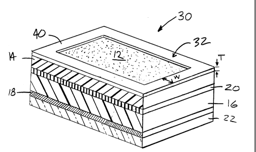
Referring to Figures 2 and 2a, the detector plate
30 in accordance with the present invention is a multi-
layered device slmllar to the prlor art detector plate 10 ln
Figure 1, except plate 30 also includes a margin 32
surrounding the periphery of transparent conductive layer
12. The margin 32 is defined by the width d of the gap
between the peripheral edge 34 of the transparent conductive
layer 12 and the peripheral edge 36 of the dielectric layer
14.
The influence of the margin 32 on arcing is more
apparent from Figure 2a which depicts a corner of the
detector plate 30. The width d of the margin 32 in effect
constitutes an increase in the distance an electrical arc
discharge must travel between the transparent conductive
layer 12 and conductlve layer 18. Slnce dlelectrlc layer 14
acts an lnsulator, the path of any dlscharge, represented by
arrow 37, ls from transparent conductlve layer 12 across the
width d of margin 32 and around the periphery of dielectric
layer 14 to conductive layer 18. It ls therefore thls
effectlve increase in distance between layers 12 and 18
resulting from margin 32 that is influential on preventlng
arclng.
21D~
60557-4762
A study was conducted to measure the effectlveness
of the margln 32 on the occurrence of arclng ln a detector
plate 30 whlch lncluded IT0 as the transparent conductlve
layer 12 coated on a polycarbonate sheet as dlelectrlc layer
14. Photoconductlve layer 16 was amorphous selenlum and the
conductlve layer 18 was an alumlnum sheet. Flve 5" X 5"
detector plates 30 were produced, deslgnated as A, B, C, D
and E ln the table of Flgure 3, by etchlng away the IT0
conductlve layer 12 of each plate 30 to provlde marglns 32
of dlfferent wldths d. The shortest margln wldth d of each
of the four sldes, deslgnated N, S, W and E, of the
respectlve detector plates ls shown ln the table of Flgure
3. The flve detector plates 30 were monltored for
electrlcal arclng ln the followlng manner. The alumlnum
conductlve layer 18 was electrlcally grounded, and a hlgh
voltage electrode was put ln contact wlth the IT0 conductlve
layer 12 of the detector plate 30. At 25% relatlve
humldlty, the voltage of the electrode was lncreased from 0
to 5 kV and was left applled to the IT0 surface of the
detector plate 30 for one mlnute. The voltage was then
lncreased ln 1 kV steps, remalnlng at each step for one
mlnute untll 10 kV had been reached. Thls procedure was
repeated for each of the five detector plates 30, and agaln
at a relatlve humldlty of 50%.
In Flgure 4, the table summarlzes the results of
thls arclng experlment. These results lndlcate that
~1~0:~9g
60557-4762
lncreasing the dlstance from the perlpheral edge 34 of the
IT0 transparent conductive layer 12 to the edge 36 of the
dlelectric layer 14 wlll reduce the llkellhood of arclng
occurrlng, and suggest the mlnlmum margln wldth d to be
about 1 cm at 50% relatlve humldlty wlthout arclng at 8 kV.
At higher humldlty condltlons that may be encountered in
practlce, thls margln wldth llkely would not be adequate and
theoretlcally may be lncreased.
However, ln practlcal terms, lt should be
understood that the cassette wlthln whlch the detector plate
30 ls to be housed ls designed to speclfled ANSI standards.
Glven such a size restrictlon, provldlng a larger margln
wldth d results ln a smaller surface area for the
transparent conductlve layer 12 and thus, a decrease ln the
effectlve lmage area of the detector plate 30. For
lnstance, ln an 18 X 24 cm detector plate and an 14 X 17
lnch detector plate, the allowable maxlmum dlstance from the
edge of the transparent conductive layer 12 to the detector
plate edge, l.e. edge of dlelectric layer 14, may be about
0.5 cm in order to maintain a reasonable amount of usable
lmage area. Ideally, lf no such slze restrictlon exlsted, a
margln 32 havlng any wldth d that was necessary to lnhlblt
arclng could be utlllzed.
Flgure 2b lllustrates an alternatlve embodlment of
the detector plate 30 whlch lncludes a second margln 39
surroundlng the perlphery of conductlve layer 18, deflned by
-- 10 --
~ 19~
60557-4762
the perlpheral edge 38 of the conductlve layer 18 belng
offset lnward of the peripheral edge 36 of the dlelectrlc
layer 14. The second margln 39 functlons to further
effectlvely lncrease the dlstance between transparent
conductlve layer 12 and conductlve layer 18 that an arc
dlscharge must travel.
To further lnhlblt the occurrence of arclng ln the
detector plate 30, as shown ln Flgure 5, an electrlcally
lnsulatlve barrler 40 ls applled ln the margln 32 around the
perlphery of the transparent conductlve layer 12. The
barrler 40 forms of a "dam" over whlch any arc dlscharge
must ~ump thereby effectlvely lncreaslng the dlstance
between layers 12 and 18. The lnsulatlve barrler 40
provldes mlnlmlzatlon of the separatlon wldth d of the IT0
layer/detector plate margln 32 and therefore asslsts ln
accommodatlng deflned cassette dlmenslons. Slllcone based
Sylgard, whlch ls a rather flexlble lnsulatlve materlal
produced by Dow Cornlng, ls the preferred materlal for the
electrlcally lnsulatlve barrler 40.
Studles were conducted ln order to flnd the
optlmum condltlons ln terms of margln separatlon wldth and
thlckness of a Sylgard lnsulatlve barrler (deslgnated as W
and T respectlvely ln Flgure 5). Referrlng to Flgure 6,
lnd~um-tln oxlde (IT0), whlch ls the preferred materlal for
transparent conductor layer 12, was coated on a
polycarbonate fllm 42 and then etched to produce two
-- 11 --
21~
60557-4762
separate IT0 layers 44 and 46 having a gap wldth W whlch was
varled durlng the experlment. A Sylgard barrler 48 was
coated between the IT0 layers 44 and 46, and the electrlcal
stablllty of the IT0 layers was then studled as a functlon
of thlckness of the Sylgard barrler 48 and humldlty. A high
voltage power supply (not shown) was connected to one of the
IT0 layers, elther 44 or 46, and the other was grounded.
The applled voltage was then gradually lncreased untll
dlscharge or IT0 breakdown occurred.
Flgure 7 ls a graph of the results from one study,
showlng the voltage dlfference at whlch IT0 breakdown
occurred for varlous thlcknesses and gap wldths of the
Sylgard coatlng. The results lndlcate that a 0.3 cm wldth
and 1.2 mm thlckness of Sylgard ls sufflclent to prevent
arclng at voltages above 10 kV, at a relatlve humldlty of
75%.
Slnce relatlve humldlty also has an lmpact on the
electrlcal fallure and the IT0 breakdown due to arclng, a
further study was carrled out ln whlch a Sylgard barrler 48
was coated between the two IT0 layers 44 and 46 keeplng the
gap wldth W constant at 0.75 cm. The IT0 breakdown (or
arclng) voltage was measured at varlous humldltles. These
results are glven ln Flgure 8 whlch reveals that a 1.2 mm
thlck Sylgard barrler 48 was sufflclent to prevent arclng at
voltages as hlgh as 10 kV.
In Flgure 9, lllustrated ls a cross sectlon
- 12 -
2~0199
60557-4762
through a corner of a conventlonal cassette 50 ln whlch ls
housed a detector plate 30. The cassette 50 ls commonly
moulded out of carbon flbre filled composlte materlals whlch
typlcally provlde a surface reslstance of about 200 ohm/sq.
Arclng posslbly mlght occur between the transparent
conductlve layer 12 and the cassette cover 54, but a
solutlon to that problem ls beyond the scope of the present
lnventlon. Accordlng to current deflned cassette
dlmenslons, the maxlmum dlstance from the surface of the
transparent conductlve layer 12 to the cassette cover 54 ls
approxlmately 1.8 mm whlch llmlts the thlckness of the
electrlcally lnsulatlve barrler 40. Based on the results
observed ln the studles dlscussed above, as a mlnlmum, a 0.3
cm wlde and 1.2 mm thlck Sylgard coatlng ls capable of
provldlng an electrlcally lnsulatlve barrler 40 that
prevents arclng when up to a 10 kV voltage dlfference ls
applled across the detector plate 30, whlle also belng able
to accommodate the 1.8 mm slze restrlctlon between
transparent conductlve layer 12 and the cassette cover 54.
It ls preferred that lnsulatlve barrler 40 be about 0.5 cm
wlde and 1.8 mm thlck. In the flnal appllcatlon, the
Sylgard lnsulatlve barrler 40 may be applled after the
detector plate 30 ls loaded lnto the cassette 50, and the
electrlcally lnsulatlve barrler 40 could functlon as a
bumper to secure the detector plate 30 wlthln the conflnes
of the cassette 50.
21~ 9
60557-4762
Turnlng now to the concern of cracklng, the
embodlment of the detector plate 60 shown ln Flgure 10, in
accordance wlth the present lnventlon, lncludes a llnear
contact 62 to connect the hlgh voltage electrode 64 from a
power supply (not shown) to the transparent conductlve layer
12. The llnear contact 62 ls fabrlcated from a more
conductive, less resistive materlal than ITO transparent
conductlve layer 12, and behaves as a gradlent through which
electrical charges flowing from the high voltage electrode
64 are dlspersed lnto the transparent conductive layer 12.
The linear contact 62 ls preferably formed as a nlckel
chromlum alloy or sllver printed strlpe posltioned generally
parallel and ad~acent an edge 66a of the transparent
conductive layer 12, and extending to near the opposing
perpendicular edges 66b and 66c of layer 12, e.g. 0.25
inches from edges 66b and 66c.
It should be understood that the width of the
linear contact 62 is restrlcted on the basis of current ANSI
standards limltlng the size of the detector plate and that
materials utilized to form the llnear contact 62 are
typically not transparent to radiatlon energy. Otherwlse,
the linear contact may be as wide as is necessary for the
particular clrcumstances, the wldth belng determined by
simple experlmentation. Therefore, ln order to minimize the
amount of unusable image area on the detector plate 60, a
linear contact 62 of about 2 mm ln wldth ls preferred.
- 14 -
19~
60557-4762
A study was conducted to measure the effect of the
linear contact 62 on preventing cracking and thus enhancing the
electrical stability of the transparent conductive layer 12.
Two detector plates, 60 and 70 shown in Figures 10 and 11
respectively, were utilized each having a 5" X 5" selenium sheet
as the photoconductive layer 16 laminated with ITO coated
polycarbonate which represent the transparent conductive layer
12 and the dielectric layer 14 respectively. The peripheral
edge 66 of the ITO coating was etched away to produce a 4" X 4"
square, thereby providing a separation margin 32 having a ~"
width between the peripheral edge 66 of the transparent
conductive layer 12 and the edge 69 of the conductive layer 18
which was a sheet of aluminum. The margin 32 is sufficiently
large so as to avoid arcing within the detector plates 60, 70
under application of a high voltage in ambient conditions (i.e.
40% relative humidity). The high voltage electrode 64 from a
power supply (not shown) is connected to the ITO transparent
conductive layer 12 and the aluminum conductive layer 18 is
grounded. The high voltage power supply may be switched on and
off through a programmable counter/relay unit.
One detector plate 60 (Figure 10) included a linear
contact 62 of approximately 3.5 inches in length, connecting the
high voltage electrode 64 to transparent conductive layer 12.
The second detector plate 70 (Figure
Z~ ~199
60557-4762
11) lncluded a conventional clrcular patch contact 72 of
several milllmetres ln dlameter. The contacts 62 and 72
were made uslng elther a sllver paste or wlth copper
conductlng adheslve foils.
Each of the detector plates 60, 70 were monltored
for cracking ln the following manner. A high voltage was
repetltlvely applled to the plate 60, 70 for 5 minutes and
swltched off for 30 seconds. Wlth the power supply swltched
off, any capacitive charge stored in the detector plate 60,
70 was dlscharged across a 50 megohm reslstor connected ln
parallel to the plate. The tlme constant of each detector
plate 60, 70 was approxlmately 35 mllllseconds, so the
plates would totally dlscharge after 30 seconds. Each plate
60, 70 was visually observed at regular lntervals to check
for cracking of the IT0 transparent conductive layer, while
the counter unlt recorded the number of cycles of voltage
appllcatlon.
In Flgure 12, the table summarlzes the results of
the cracking experiment. These results indicate that the
conventlonal clrcular patch contact 72 damaged the IT0
transparent conductlve layer 12 with less than 600 cycles at
voltages above 8 kV. The dlstrlbuted llnear contact 62,
however, ylelded very hlgh cycllng llfe-tlmes ln excess of
12,000 cycles even at lO kV. Therefore, the transparent
conductlve layer 12 was found to be more stable with the
linear contact 62.
- 16 -
- 21~01~39
60557-4762
Referring to Flgure 13, to further prevent break
down of the transparent conductlve layer 12, ln partlcular
at the corners thereof, the transparent conductlve layer 12
may lnclude smooth or arcuate corners 74. Although lt would
be advantageous to provlde arcuate corners 74 havlng a
larger radlus, ln practlcal terms, to accommodate more
lmaglng area ln the detector plate 76 a preferable radlus ls
about 5 mm.
- 17 -