Note: Descriptions are shown in the official language in which they were submitted.
W O 94~7777 21 4 0 25 3 PCTAUS94/03730
~_ 1
,~ ,.. .
TIN-BISMUTH SOLDER PASTE AND METHOD OF USE
Background of the Invention
This invention relates to a solder paste for forming a tin-
bismuth solder connection having enh~nced high temperature
10 properties. More particularly, this invention relates to a solder
paste that comprises a m~ re of tin-bismuth alloy powder and a
powder of a tertiary metal, ~,le~ably gold or silver, effective to
enh~nce the high temperature properties of the product connection.
Solder paste is employed to form a solder connection, for
15 example, for surface mollntin~ a component to a printed circuit
board or the like. A typical paste comprises a powder formed of a
solder alloy and dispersed in a liquid vehicle that contains a flux.
The vehicle may also comprise an expendable organic binder to
hold the powder in a self-sust~inin~ mass following application. To
2 0 form the connection, the board features a solder-wettable bond pad
that constitutes a first faying surface. ~~imil~rly, the component
includes a second, solder-wettable faying surface, for example, a
contact. The solder paste is conveniently applied to the bond pad,
for example, by screen printing, after which the component is
2 5 arranged with the second faying surface in contact with the solder
paste deposit. The ~csemhly is then he~te~l to vaporize the vehicle
and to melt and reflow the solder alloy. Upon cooling, the solder
alloy resoli~ifies and bonds to the faying surfaces to complete the
connection. The solder connection not only physically att~ches the
3 0 component to the board, but also electrically co~nects the bond pad
on the board and the contact of the component for cor ~ n~
electrical ~; lrle~t to or from the component for procesginE~.
Common solder is formed of tin-lead alloy. It is proposed to
form a lead-free solder connection composed of tin-bismuth alloy.
3 5 Howev~r, tin-bismuth alloy tends to exhibit poor meçh~nic~l
WO 941277M PCT/US94/03730
2140253
properties at elevated tempelal-lles of the type encountered by
microelectronic packages during use. In particular, such solder
alloys tend to become lln~cceptably soft at tempe~tu~as as low as
100~ C and exhibit a relatively low melting temperature,
S particularly in comparison to the common tin-lead solders.
Sllmm~ry of the Invention
This invention contempl~tes a solder paste that includes a
mi~tllre of compositionally distinct metal powders that alloy to form
the solder connection. Thus, the paste comprises a first metal
powder that is formed of tin-bismuth solder alloy. The paste further
comprises a second metal powder composed of a tertiary metal
1 5 effective to increase the meltinF tem~era~u~e and improve the
merhs~nic~l properties of the tin-bismuth alloy. r}efe~ed tertiary
metal is gold or silver. In particular, it has been found that
additions of gold between about 1.0 and 2.2 weight percent are
effective to .signific~ntly improve the desired high temperature
2 0 properties of the resulting connection.
In one aspect of this invention, a method is provided for
forming a solder connection between solder-wettable faying
surfaces, for example, between a bond pad of a printed circuit board
and a contact of a compo~e~t The method comprises arr~nginF
2 5 the faying surfaces in contact with a deposit of the solder paste
cont~ininE the mixture tin-bismuth solder alloy powder and the
tertiary metal powder. The ~ssemhly is he~te~l to melt the tin-
bismuth solder alloy. Upon melting, the tin-bismuth powder
coAlesces to form a liquid solder that forms the basis for the solder
3 0 connection. Concurrently, the tertiary metal of the second powder
dissolves into the solder liquid. Upon cooling, the solder liquid
soli~ifies and bonds to the faying surfaces to complete the solder
connection. The solder connect;on exhibits enh~nse-l high
temperature mech~nic~l properties, including an increased
WO g4127777 2 1 4 ~ 2 ~ 3 PCT/US94/03730
_ 3
melting temperature, as a result of the alloying of the tertiary metal
with the tin-hi.cmllt~l alloy.
S Brief Description of the Drawings
The present invention will be further illustrated with
~afelellce to the accompanying drawings wherein:
FIG. 1 is a cross-sectional view of an ~semhly of a printed
10 circuit board and an electrical component with a solder paste in
accordance with this invention;
FIG. 2 is a cross-section~l view of the ~semhly in FIG. 1
following solder reflow to form a solder coI nection;
FIG. 3 is a graph showing melting temperature as a function
1 5 of gold content in tin-bismuth solder alloy; and
FIG. 4 is a graph showing Knoop hardness as a function of
temperature for several solder alloys, including gold-cont~ining
tin-bismuth alloy formed from solder paste in accordance with this
invention.
Detailed Description of the P~efel~ed Embo-liment
In a preferred embo~iment, the solder paste in accordance
2 S with this invention is employed to form a lead-free solder
connection for mounting an electrical component onto a printed
circuit board. The paste is suitably formulated by ~ ition of gold
powder to commercial solder paste Cont~ininE tin-bismuth solder
powder. Preferred tin-bismuth solder powder consists of a near
3 0 eutectic alloy composed of about 60 weight percent bismuth and the
bs~l~n~e tin, and cQ~t~in~ less than 0.1 percent lead as impurity.
The tin-bismuth powder was sized belwee~ -200 and +325 mesh and
is dispersed in a vehicle. The vehicle is compose~l of high boiling
~lcoh~ and glycol solvent and contains a flux consisting of a white
3 5 rosin compound. The paste also includes an e~pentl~hle organic
wo 94~27777 PCTIUS9S.!~)3/~0
2140253 4
binder, suitably ethyl cellulose compound, effective to bond the
powder into a cohesive deposit. Suitable paste is commercially
available from Indium Corporation of America under the trade
~lesi~n~tion Indalloy 281. Gold powder is added to the tin-bismuth
5 solder paste to formulate the paste in accordance with this
invention. The gold powder featured particles having ~imens;ons
between about 5 and 10 ~icrons. The gold addition was calculated
based upon the total weight of metal powder and is l.~efelably
between about 1.0 and 2.2 weight percent.
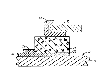
Referring to FIG. 1, there is depicted an assembly for
mounting a discrete component 10, such as a resistor or the like, to
a printed circuit board 12 u~ ing solder paste in accordance with
this invention. Printed circuit board 12 comprises a metallic copper
trace 16 ~ffi~(l to a ~3ielectric substrate 18 ofthe type lefe.-led as an
1 5 FR4 card and composed of an epoxy resin and glass fiber l~min~te.
Trace 16 includes a surface mount pad 20 that is the site for
att~hing component 10. Board 12 further comprises a solder stop
22 composed of an epoxy-base or other suitable polymeric resin that
provides a solder-nonwettable barrier. Solder stop 22 is applied to
2 0 trace 16 to block the spread of solder alloy and thereby co~fine the
solder alloy to bond pad 20 during reflow. A deposit 24 of the solder
paste comprising the mixture of tin-bismuth solder powder and
gold powder is applied to bond pad 20 by screen printing.
Component 10 comprises a contact 30 formed of palladium-silver
2 5 alloy, which constitutes a faying surface for the connection.
Following deposition of the solder paste 24, component 10 is
~sembled with printed circuit board 12 such that contact 30 is in
contact with deposit 24.
To complete the connection~ the assembly shown in FIG. 1 is
3 o he~te~l to a tempelatul~ greater than 140~ C, and l~refelably greater
than 160~ C, to reflow the solder alloy. During the initial stages of
he~ing, residual solvent and organic binder in the deposit 24 are
tlecomposed and vaporized. As the assembly is he~te~l above about
138.5~ C, the eutectic mel~ing tempelalu~, the tin-bismuth
3 5 particles dissolves and coalesce to produce a liquid phase.
5 ~ 7 ~
..".,.
Concurrently, the liquid phase commencçs to melt the gold powder.
At the elevated temperature, a uniform liquid forms that wets bond
pad 20 and cont~ct 30. Wetting is facilitated by the activity of the
white rosin fluY. The ~ss~mhly is cooled to produce solder
S connection 32 in FIG. 2 that bonds to bond pad 20 and to contact 30
and ~Yten~c continuously there between to attach component 10 to
board 12 and also to electrically connect pad 20 and co~t~- t 30.
Connection 32 is composed subst~n~lly of tin and bismuth derived
from the solder alloy of the first metal powder and cont~inc gold
derived from the second metal powder, ~ere,ably in an amount
between about 1.0 and 2.2 weight ~el~ellt.
Thel~roLe, this i~v~Illion provides a solder paste that
includes a m~ re of metal powders dispersed in a vaporizable
vehicle. The mixture is formed predomin~ntly of powder composed
1 5 of a solder alloy of tin and bismuth. In general, tin alloys
cont~ining between about 30 and 70 weight percent bismuth have
melting temperatures suitably low to permit reflow onto
conventional substrate material like epoxy-base printed circuit
boards, and are readily available in high purity that is subst~ntially
2 0 free of lead. The prefe~led alloy contains between about 48 and 68
weight percent bismuth. OptionalIy, the initial solder powder may
include small amounts, typically less than 4 weight percent, of other alloy agents
to enh~nce mechanical properties. The paste further comprises a
minor addition of a second metal powder cont~ining a tertiary
2 5 metal to enhance mechanical properties of the tin-bismuth solder.
Suitable tertiary metals for alloying with the tin-bismuth solder
include gold and silver, with gold being preferred. Although the
~lere~led embodiment the second metal powder is composed of the
tertiary metal in neat form, the metal may be prealloyed, including
3 0 with tin or bismuth. During heating to reflow the solder paste, the
tin-bismuth powder initially melts and reflows. It is a significant
advantage of this invention that the reflow Gf the tin-bismuth solder
commences at a relatively low temperature, significantly less than
the gold-cont~ining alloy that forms the connection. This promotes
3 5 wetting of the faying surfaces during the early stages of reflow,
which wetting is essenti~l to formation of a strong solder bond.
Nevertheless, the tertiary metal ev~lllually dissolves into the liquid
phase and alloys with the tin and bismuth to form a connection
having enh~nced high temperature properties.
S FIG. 3 is a graph showing melting temperature as a function
of gold concent~ation in alloy composed of 58 weight percent
bismuth and the b~l~nce tin. As can be seen, conce..t~ations of gold
of as little as 1 weight percent .ci~nific~ntly increase the melting
tempe~dluLe of the alloy. Concentrations ~r~ater than about 2.2
1 0 weight percent have melting tempe- d(,U~ es above about 210~ C. In
common practice solders are reflowed at temperatures that are 20~
C to 40~ C above the melting tempe~d~u~e to ~ccRlerate melting and
reduce cycle time. Accordingly, alloys cont~ining greater than
about 2.2 weight percent gold necessitate high reflow tempe~dlu~es
1 5 that tend to ~l~m~ge other features typically found in electronic
packages. Also, at higher gold co~ce..l..alions, the formation of tin-
gold intermetallic phases becomes sig~uficant and tends to
~liminich the mechanical properties of the connection. A preferred
gold concentration in the product connection is between about 1.0
2 0 and 2.2 weight percent gold.
FIG. 4 shows a plot of Knoop hardness in grams per micron
as a function of temperature. Curve A indicates new hardness for
an alloy comprising of about 2.0 weight percent gold, 58 weight
percent bismuth and the b~l~nce tin, which alloy is produced by
2 5 paste formulated in accordance wiih this invention. For purpcses
of comparison, curve B shows hardness for a comparable tin-
bismuth alloy without gold, whereas curve C represents a standard
tin-lead solder alloy composed of about 2 weight percent silver,
about 36 weight percent lead and the balance tin. As can be seen,
3 0 the gold addition substantially increases the hardness of bismuth-
tin solder alloy at elevated temperatures and produces a hardness
comparable to tin-lead alloy within the range of about 110~ C to 150~
C. In general, hardness is believed to indicate increased strength,
so that tin-bismuth-gold alloy derived from paste in accordance
3 S with this invention result in stronger, more durable connections
~. '
-~ L
that are better able to withsta~d temperature t~ ions of the type
experience~ by microelectronic p~k~ges during use.
Although FIGs. 3 and 4 ~erlai~ to gold additions to tin-
bismuth alloy, a simil~r increase in the melting temperature of tin-
S bismuth alloy is believed to be obtained using silver additions.
Accordingly, silver may be suitably substituted to enh~nce the high
temperature property of connPc~;onc formed of alloys of tin and
bismuth.
In the described embo-limPnt solder paste formulated to
10 contain a gold addition in accordance with this i~vt~llLion was
employed for mounting a discrete comronent to a printed circuit
board. During reflow, the metal powders of the solder paste
co~lesced to form a solder liquid that wet a first faying surface that
is the bond pad of the printed circuit board and a secnnd faying
1 5 surface that is the contact of the component, and, upon cooling,
solidified to form the desired solder connection. Although copper
and pl~l.;..,....-silver alloy were selected for the faying surfaces, the
faying surface may be suitably formed of nickel or any other metal
that is solder-wettable so as to produce a strong solder bond. Still
2 0 filrther, this invention may be readily adapted to form solder bump
connections between a substrate, such as a printed circuit board or
ceramic chip carrier, and a bond pad located on an integrated
circuit chip.
While this invention has been described in terms of certain
2 5 embo~imentc thereof, it is not intentle-l to be limited to the above
description, but rather only to the extent set forth in the claims that
follow.