Note: Descriptions are shown in the official language in which they were submitted.
~1~03~ ~958
21/22
DESCRIPTION
ANTENNA OF WAVEGUIDE STRUCTURE AND
METHOD OF MANUFACTURING THE SAME
TECHNICAL FIELD
The present invention relates to an antenna of
a waveguide structure and a method of manufacturing the
same, and more particularly to an antenna of a leaky
waveguide structure and a method of manufacturing the
same.
BACKGROUND ART
An antenna of a waveguide structure is
generally known as an example of an antenna used for
receiving satellite broadcasting. This antenna is
provided with a radiation plate, in which slots are
formed at predetermined intervals for performing
transmission-reception of electromagnetic waves in a
band having a central frequency of 11.85 GHz effici-
ently, and a plurality of parallel waveguides providedunder the radiation plate for transmitting the
electromagnetic waves.
An antenna of a leaky waveguide structure that
is a sort of the antenna described above is constructed
of a main body and a radiation plate made of a metal
such as aluminum or copper. The main body includes one
flat bottom plate and a plurality of elongated rectan-
~403fi~
gular sidewalls fixed perpendicularly to the bottomplate. The radiation plate is made of a flat plate and
arranged in parallel to the bottom plate with a given
distance therebetween so as to provide a space between
one surface of the bottom plate and one surface of the
radiation plate. The plurality of sidewalls serve as
partitions for separating the space into one elongated
feed waveguide and a plurality of parallel radiation
waveguides, each conducting at its one end with the feed
waveguide. Thus, one side in a longitudinal direction
of each sidewall is fixed to the one surface of the
bottom plate, and an opposite side thereof is fixed to
the one surface of the radiation plate so that the one
feed waveguide and the plurality of radiation waveguides
separated by the sidewalls are formed in the space
between the bottom plate and the radiation plate.
Further, a plurality of slots are formed at a part of
the surface of the radiation plate facing to each
radiation waveguide. An antenna of a leaky waveguide
structure constructed as mentioned-above is described
in, for example, the following documents.
(1) Furukawa et al.: "Beam-Tilt Planar Waveguide Slot
Antenna of Single Layer Structure for Satellite TV", The
Institute of Electronics and Information Communication
Engineers in Japan, AP88-40. July 1988.
(2) Hirokawa et al.: "Design of a Crossed Slot Array
Antenna on a Leaky Waveguide", The Institute of
Electronics and Information Communication Engineers in
~14~36~
Japan, AP92-37. May 1992.
(3) Kiyohara et al.: "An Analysis and a Design of
Cross Slots for a Leaky-wave Antenna", The Institute of
Electronics and Information Communication Engineers in
Japan AP91-75. September 1991.
(4) Hirokawa et al.: "Single-Layer Slotted Leaky
Waveguide Array for Mobile DBS Reception", Technical
Report of IEICE AP93-25, SAT 93-8. 1993-05.
(5) Japanese Patent Application No. 5-276152 (U.S.
Patent Application No. 08/169/215, Canada Patent
Application No. 2,111,394, Korea Patent Application No.
24577.93 and Taiwan Patent Application No. 82109579
correspond thereto, respectively.)
In an antenna of a conventional waveguide
structure, the radiation plate and the waveguides have
been connected to each other by fixing the radiation
plate to the sidewalls of the waveguides by screws.
Riveting and caulking may be used as another means for
connecting the radiation plate with the waveguides. In
these conventional methods, however, production steps
are increased. Further, each sidewall has to be made
thicker sufficiently to provide a space for screw
clamping or riveting and to prevent distortion caused by
clamping force thereof. Similarly, the radiation plate
has also to be made thicker for security of the strength
in screw clamping or the like and prevention of distor-
tion. For reason of the foregoing, the antenna becomes
expensive and the weight thereof is increased. As a
21433~0
-- 4
result, it becomes difficult to obtain desired perform-
ance of the antenna. Furthermore, excessive thickness
of the sidewalls and the radiation plate causes the
necessary power of a driving control portion to increase
and makes miniaturization of the device difficult when
the antenna is used as a mobile antenna with a tracking
mechanism or the like. Further, the distortion incurs
lowering of transmission efficiency of the waveguide.
DISCLOSURE OF INVENTION
It is an object of the present invention to
provide an antenna of a waveguide structure that is
light in weight and has less distortion and simple in
its manufacturing method and a method of manufacturing
the same.
According to one aspect of the present
invention, an antenna of a waveguide structure includes
a flat thin metallic bottom plate; a flat thin metallic
radiation plate arranged in parallel to the bottom plate
with a certain interval from the bottom plate so as to
provide a space between the bottom plate and the radia-
tion plate; and a plurality of flat and thin metallic
sidewalls disposed in the space and fixed to the bottom
plate and the radiation plate so as to separate the
space between the bottom plate and the radiation plate
into a plurality of waveguides conducting with one
another; wherein the radiation plate is joined to the
plurality of sidewalls by a plurality of spot welds at
~:~.40~6~
predetermined intervals.
According to another aspect of the present
invention, an antenna of a waveguide structure includes
a flat thin metallic bottom plate; a flat thin metallic
radiation plate arranged in parallel to the bottom plate
with an interval from the bottom plate so as to provide
a space between the bottom plate and the radiation
plate; and a plurality of flat and thin metallic
sidewalls disposed in the space and fixed to the bottom
plate and the radiation plate so as to separate the
space between the bottom plate and the radiation plate
into a plurality of waveguides conducting with one
another; wherein the plurality of sidewalls are formed
into a single block of metallic material integrally with
the bottom plate.
According to one aspect of the present
invention, a method of manufacturing an antenna of a
waveguide structure, which includes a flat thin metallic
bottom plate; a flat thin metallic radiation plate
arranged in parallel to the bottom plate with an
interval from the bottom plate so as to provide a space
between the bottom plate and the radiation plate; and a
plurality of flat and thin metallic sidewalls arranged
in the space and fixed to the bottom plate and the
radiation plate so as to separate the space between the
bottom plate and the radiation plate into a plurality of
waveguides conducting with one another, includes the
step of joining the radiation plate to each of the
214~
plurality of sidewalls by laser welding.
According to another aspect of the present
invention, a method of manufacturing an antenna of a
waveguide structure, which includes a flat thin metallic
bottom plate; a flat thin metallic radiation plate
arranged in parallel to the bottom plate with a certain
interval from the bottom plate so as to provide a space
between the bottom plate and the radiation plate; and a
plurality of flat and thin metallic sidewalls disposed
in the space and fixed to the bottom plate and the
radiation plate so as to separate the space between the
bottom plate and the radiation plate into a plurality of
waveguides conducting with one another, includes the
step of forming the bottom plate and the plurality of
sidewalls fixed to the bottom plate in a form of a
single block of metallic material.
Aluminum, copper or the like is used as the
material of a main body including the bottom plate and a
plurality of sidewalls and that of the radiation plate.
In particular, aluminum is preferred in its workability
and electrical characteristics. Further, it is desired
to plate an inner surface of the waveguide with gold or
silver in order to increase the transmission efficiency.
A solid-state laser such as YAG laser and ruby laser is
suitable for laser welding. Spot welding performed at a
predetermined pitch is desired for laser welding. In
this case, it is desired to set the pitch of the spot
welding to 1/10 or less of the wavelength of the used
~ 1 ~ 0 3 6 0
-- 7
electromagnetic wave (2.6 mm or less in the case of
11.85 GHz). This is because the substantially same
effect as that obtained in continuous welding can be
obtained.
Further, the main body is preferably produced
by casting. When the main body is produced by casting,
it is possible to make the main body highly in precise
at a low price. A die casting method, a lost wax
method, a shell mold method or the like is suitable as
the casting method. When the laser welding is performed
from the top surface of the radiation plate, welding
workability is excellent. When the laser welding is
performed while forming a conical dent in advance at
each welding position by punching or the like, it is
possible to save the necessary power of laser and also
to prevent excessive welding metal from swelling on a
radiation surface. The m~ximum diameter and the depth
of the dent are suitably about 1/3 to 1/2 and 1/4 to 1/2
of the thickness of the radiation plate, respectively.
Since the heat is concentrated on a very small
point in laser welding, it is possible to fix the main
body to the radiation plate by a small amount of weld
metal, and distortion caused by welding becomes less.
Therefore, it is possible to make the sidewalls and the
radiation plate thinner.
2 ~ 4~ 360
- 7a -
In the lost wax casting method, the model of
an object to be cast is first made of wax and the wax
model is embedded into a molding sand to make a mold of
the object. Then, the mold with the wax model embedded
therein is heated to cause the wax model to melt and
flow out of the mold thereby making a cast mold with a
cavity having a shape of the object. A metal cast of
the object is made by pouring a molten metal into the
mold.
In the shell mold method of casting, a mix of
silica sand and thermosetting resin particles of
carbonic acid is coated on a heated metallic model of
an object to be cast thereby making a pair of shell
molds made of a thin plate of the harden thermosetting
resin. A cast mold of the object is made by connecting
the pair of shell molds by adhesive agent.
BRIEF DESCRIPTION OF DRAWINGS
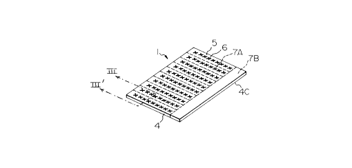
Fig. 1 is a perspective view showing an
21403~0
external appearance of an antenna of a leaky waveguide
structure according to one embodiment of the present
invention;
Fig. 2 is a perspective view showing a
structure of a main body of the antenna of a leaky
waveguide structure shown in Fig. 1;
Fig. 3 is a sectional view taken along a line
III-III in Fig. l;
Fig. 4 is an enlarged sectional view showing
an example of a spot weld between a radiation plate and
a sidewall;
Fig. 5 is an enlarged sectional view showing
another example of a spot weld between a radiation plate
and a sidewall;
Fig. 6 is a perspective view showing an
external appearance of an antenna of a leaky waveguide
structure according to another embodiment of the present
invention; and
Fig. 7 is a perspective view showing the
structure of the main body of the antenna of a leaky
waveguide structure shown in Fig. 6.
BEST MODE FOR CARRYING OUT THE INVENTION
An embodiment of the present invention will be
described with reference to Fig. 1 to Fig. 4. Fig. 1 is
a perspective view showing an exterior configuration of
an antenna of a leaky waveguide structure according to
an embodiment of the present invention. The external
2140360
appearance of an antenna of a waveguide structure
according to the present invention is not different
basically from a conventional unit. Namely, an antenna
1 of a waveguide structure is manufactured with a main
body 2 and a radiation plate 5 made of a metallic
material such as aluminum or copper. As shown in Fig. 1
and Fig. 3 showing a section taken along a line III-III
in Fig. 1, the main body 2 includes a flat bottom plate
3 and a plurality of sidewalls 4A, 4B and 4C each being
formed of a substantially rectangular elongated thin
plate. The bottom plate 3 and the sidewalls 4A, 4B and
4C are made of aluminum integrally in one block by
casting, e.g. by a die casting method. Each sidewall
includes upper and lower sides 4a and 4b parallel to a
longitudinal direction, and the lower side 4b is
integrally connected to the bottom plate 3 so as to hold
the sidewall perpendicular to the bottom plate. As
shown in Fig. 2, the sidewalls 4A are arranged parallel
to one another, and include long sidewalls and short
sidewalls disposed alternately one another. The
sidewalls 4B are arranged along a traverse direction at
a right angle to the longitudinal direction of each
sidewall 4A with predetermined intervals between them,
and the central part of each sidewall 4B is integrally
connected to an end portion of the elongated sidewall
4A. The sidewall 4C is arranged parallel to the
sidewalls 4B.
The radiation plate 5 is made of a flat plate
~1~03~
-- 10 --
of aluminum and arranged parallel to the bottom plate 3
so as to provide a space between the bottom plate 3 and
the radiation plate 5. One surface of the radiation
plate 5 is fixed to the upper sides 4a of the sidewalls
4A, 4B and 4C at a plurality of points by spot welding.
With this, the space between the bottom plate 3 and the
radiation plate 5 is separated by the sidewalls into a
plurality of waveguides communicated mutually with each
other and disposed in predetermined pattern. Namely,
radiation waveguides 7A parallel to one another are
formed each defined by two adjacent sidewalls 4A, the
bottom plate 3 and the radiation plate 5, and a feed
waveguide 7B extending in a direction at a right angle
with the radiation waveguides is formed between the
sidewalls 4B and the sidewall 4C. The feed waveguide 7B
is branched into adjacent two of the radiation wave-
guides 7A through each gap 18, thus forming a ~ branch.
Cross slots 6 are formed at a part of the radiation
plate 5 facing to each of the radiation waveguides 7A
with predetermined intervals in the longitudinal direc-
tion of the waveguide. Further, inductive posts 10 are
provided at positions on the bottom plate 3 facing to
the feed waveguide 7B corresponding to the ~ branches.
These posts 10 are made of aluminum integrally with the
bottom plate 3. The radiation waveguide, the feed
waveguide, the inductive post, the ~ branch and the
cross slot described above are all well known. Since
detailed description thereof is made in the document (4)
~14~36~
mentioned above, it is requested to refer to the same.
The thickness of the bottom plate 3 is 1.5 mm,
and the thickness of the radiation plate 5 is 0.3 mm.
Each of the sidewalls 4A, 4B and 4C has a thickness of
1.0 mm, and a height, i.e., the distance between
parallel sides 4a and 4b of 4.0 mm. Further, the
distance between adjacent two sidewalls 4A, i.e., the
width of the radiation waveguide 7A is 17 mm, and the
distance between the sidewall 4B and the sidewall 4C,
i.e., the width of the feed waveguide 7B is 34 mm.
The spot welding between the upper side 4a of
each sidewall and the radiation plate 5 is made
preferably by laser spot welding. The upper surface of
the radiation plate 5 is irradiated with energy of 8
joules (Kw-msec) of YAG laser having the wavelength of
1.06 ~m, thereby to spot weld the radiation plate to the
upper side of the sidewall at intervals of 2.5 mm pitch.
As shown in Fig. 4, the part irradiated with laser is
melt so as to form a weld metal 8 thereby connecting
fixedly the upper side 4a of the sidewall 4A to the
radiation plate 5.
When an electromagnetic wave of 11.85 GHz is
supplied to the antenna 1, the electromagnetic wave is
transmitted outside through the feed waveguide 7B, the
gaps 18, the radiation waveguides 7A and the slots 6.
Fig. 5 shows a typical section of a weld when
welding is made by another spot welding method. In this
spot welding, a dent 9 having a conical section is
~ ~ ~ Q 3 6 ~ '
- 12 -
formed by punching in advance at an upper portion of the
radiation plate 5 opposite to the spot-welding position
and the spot-welding is applied to the portion of the
dent 9. In this case, the applied power of the laser is
decreased, and it is possible to prevent excessive weld
metal 8 from swelling on the upper surface of the
radiation plate as shown in Fig. 4.
Next, another embodiment of the present
invention will be described with reference to Fig. 6 and
Fig. 7.
In this embodiment, an antenna 11 of a
waveguide structure also includes a main body 12 and a
radiation plate 15 made principally of aluminum like in
the embodiment shown in Fig. 1 and Fig. 2. The main
body 12 is provided with a flat bottom plate 13 and a
plurality of substantially rectangular elongated thin
sidewalls 14A, 14B and 14C. The bottom plate 13 and
the sidewalls 14A, 14B and 14C are made of aluminum in
one block by casting, e.g., by a die casting method.
Each sidewall includes upper and lower sides 14a and
14b parallel to each other in the longitudinal
direction, and the lower side 14b is integrally
connected to the bottom plate 13 in a block so as to
hold the sidewall perpendicularly the bottom plate.
The sidewalls 14A are arranged parallel to one another
in the longitudinal direction with predetermined
intervals, as shown in Fig. 7. The sidewalls 14B are
arranged along a direction being at a right angle to
the longitudinal direction of the sidewalls 14A
3 ~
with predetermined gaps 20 therebetween. The central
part of each sidewall 14B is integrally fixed to the end
portion of one sidewall 14A. The sidewall 14C is
arranged parallel to the sidewalls 14B.
The radiation plate 15 is made of a flat
aluminum plate and arranged parallel to the bottom plate
13, and one surface thereof is fixed to the upper sides
14a of the sidewalls 14A, 14B and 14C by spot welding.
With this, a radiation waveguide 17A is defined by
adjacent two sidewalls 14A, the bottom plate 13 and the
radiation plate 15, and a feed waveguide 17B is formed
between the sidewalls 14B and the sidewall 14C. The
feed waveguide 17B communicates with the radiation
waveguides 17A through gaps 20, respectively. Cross
slots 16 are formed at predetermined intervals along
two lines in the longitudinal direction of the
waveguide at a part of the radiation plate 15 facing
each radiation waveguide 17A.
The thickness of the bottom plate 13 is 1.5
mm, and the thickness of the radiation plate 15 is 0.3
mm. Each of the sidewalls 14A, 14B and 14C has a
thickness of 1.0 mm, and a height, i.e., the distance
between parallel sides 14a and 14b is 4.0 mm. Further,
the distance between adjacent two sidewalls 14A, i.e.,
the width of the waveguide 17A, and the distance between
the sidewall 14B and the sidewall 14C, i.e., the width
of the waveguide 17B are both 17 mm.
The spot welding between the upper side 14a of
;~
3 ~i ~
- 14 -
each sidewall and the radiation plate 15 is made prefer-
ably by laser spot welding. The top surface of the
radiation plate 15 is irradiated with a YAG laser beam
having a wavelength of approximately 1.06 ~m at energy
of approximately 8 joules (Kw-msec), thereby to spot
weld the radiation plate to the upper side of the
sidewall at intervals of 2.5 mm pitch.
When an electromagnetic wave of 11.85 GHz is
supplied to the antenna 11, the electromagnetic wave is
transmitted outside through the feed waveguide 17B, the
gaps 20, the radiation waveguides 17A and the slots 16.
In an antenna of a waveguide structure and a
method of manufacturing the same according to the
present invention, since the sidewalls and the radiation
plate are connected fixedly to each other by laser
welding, it is possible to connect the main body and the
radiation plate fixedly to each other with a small
amount of weld metal. Accordingly, production steps are
reduced and the sidewalls and the radiation plate can be
made thinner as compared with a conventional method such
as screw clamping, so that it is possible to make a
lightweight antenna at a low price. Further, since the
sidewalls are formed thin with less deformation in
connection between the sidewalls and the radiation
. plate, the flatness of the internal surface of the
21~0360
waveguide is high and the transmission loss of the
electromagnetic wave is small.