Note: Descriptions are shown in the official language in which they were submitted.
- 214039~
72057-35
INSTRUMENT FOR PRODUCTION OF SEMICONDUCTOR
DEVICES AND PROCESS FOR PRODUCTION THEREOF
Background of the Invention
(1) Field of the Invention
The present invention relates to instruments for
production of semiconductor devices such as integrated circuits
as well as to a process for producing such instruments.
(2) Description of the Prior Art
The production of semiconductor devices consists of
many steps and consequently, various instruments are used for
each production step; however, conventional instruments have
some problems.
A jig for semiconductor
For example, in the steps for semiconductor element
production, such as a plasma etching step, an epitaxy step and
the like, it is very important that when a semiconductor wafer
makes contact with, for example, a jig used in the production
steps, the semiconductor wafer is neither stained nor damaged
and the properties of the resulting semiconductor device are
not impaired.
The semiconductor wafer, therefore, is handled very
carefully. For example, when the semiconductor wafer is trans-
ferred from one step to the next step, the semiconductor wafer
is supported by a jig for transfer, such as a wafer hand, wafer
holder or the like.
These jigs for semiconductor wafers have heretofore
been made of a material such as metal, silicon carbide, silicon
oxide, zirconium oxide, Teflon (Trade-mark) or the like. The
21~0395
_ 72057-35
jigs made of such materials have caused various problems during
contact with the semiconductor wafer.
For example, metals each become a direct staining
source for the semiconductor wafer; silicon oxide and zirconium
oxide each have a high hardness, are difficult to process,
damage the semiconductor wafer, and are expensive; silicon
carbide has a high hardness, is difficult to process with high
precision, has a low material purity, and causes staining; and
Teflon has a problem in purity of material and is difficult to
obtain in a high purity.
A semiconductor wafer dummy
As semiconductor integrated circuits have become
finer, with a higher degree of integration and higher density,
a plasma etching technique capable of forming a more precise
and finer pattern has become more necessary. In this plasma
etching, a high-frequency electric current is applied between
electrodes to generate a plasma, and a silicon wafer is etched
by the plasma. The free radicals and ions of halogen-based
gas present in the plasma are attracted by the electric field
inside an etching chamber and hit the wafer placed on the
opposing electrode, whereby the wafer is etched.
When the above etching is repeated in the chamber of
a plasma etching apparatus, the etched silicon and other
substances are deposited and adhered on the chamber inside wall,
the wafer holder, etc. Therefore, the removal of the deposited
or adhered silica, etc. by cleaning becomes necessary.
Currently, however, this cleaning is done manually and is
21g~39S
72057-35
generally conducted by wiping off the silicon, etc. by using,
for example, a special cloth for semiconductor material.
The above manual cleaning by using, for example, a
special cloth for semiconductor material to wipe off the
silicon, etc. requires a long time in cleaning operation and
includes a high possibility of secondary staining with human
sweat. For these reasons, development of a new cleaning method
has become necessary.
In order to solve the above problems, there was
proposed a method which comprises fixing, in a plasma etching
chamber, a material resistant to plasma etching as a dummy for
a silicon wafer, and generating a plasma in the chamber to
remove the deposited silicon, etc. by etching. As the material
resistant to plasma etching, usable as a dummy for a wafer,
there were studied quartz, silicon carbide, graphite and the
like.
However, these materials have problems. That is,
quartz cannot be used as a dummy because of the insulation;
silicon carbide is expensive and is difficult to process and
obtain at a high purity; and graphite has a detrimental drawback
of powder detachment and cannot be used as a dummy although it
is inexpensive and can easily be processed and obtained at a
high purity.
Boats for supporting semiconductor wafers
Boats for supporting semiconductor wafers are used
for various purposes such as (1) supporting of semiconductor
wafers thereon, (2) prevention of detachment of said wafers in
~1~039~
~ 72057-35
diffusion treatment in a diffusion furnace and (3) transfer of
said wafers before and after diffusion treatment. As semi-
conductor devices have become integrated more highly and have
come to possess higher performances in recent years, a
necessity has become stronger for a boat for supporting semi-
conductor wafers which is resistant to a heat treatment at high
temperatures and which can be produced easily at a high purity.
Conventional boats for supporting semiconductor wafers
include, for example, a boat described in Japanese Patent
Application Kokai (Laid-Open) No. 60-107843. In this boat,
however, since the constituent members are made of quartz or
silicon, there occur strain, cracking and chipping during the
formation of grooves (e.g. rod grooves for supporting wafers);
as a result, semiconductor wafers are rubbed against the
defective portions of rods, resulting in generation of dust,
damaging of wafers, and appearance of dislocation defects in
wafers.
Object and Summary of the Invention
The object of the present invention is to provide
instruments for production of semiconductor devices which are
free from the above-mentioned problems of the prior art, as well
as a process for producing such instruments.
Another object of the present invention is to provide
a jig for semiconductor devices which can protect a semi-
conductor wafer from being stained or damaged, and which can be
produced easily at a high purity and at a low cost.
Another object of the present invention is to provide
a boat for semiconductor wafers which generates essentially no
21403g5
- 72057-35
dust, and which can be produced easily at a high purity and at
a low cost.
Still another object of the present invention is to
provide a semiconductor dummy used in plasma etching which can
easily be processed and obtained at a high purity and at a low
cost, and which causes essentially no powder detachment.
The present invention provides: an instrument for
production of semiconductor devices, which is composed
substantially of a vitreous carbon derived from polycarbodi-
imide resin, and a process for producing an instrument for
production of semiconductor devices which comprises molding a
polycarbodiimide resin or a composition composed mainly of a
polycarbodiimide resin, into a shape of an instrument for
production of a semiconductor device and then carbonizing the
molded material.
Brief Description of the Drawings
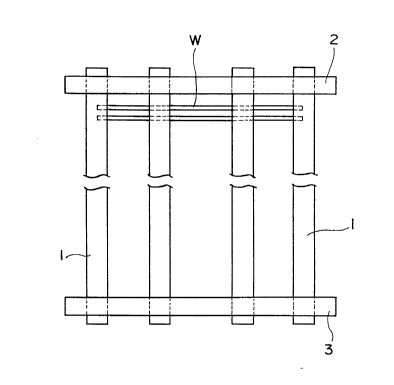
Figure 1 is a side view of an example of the boat for
supporting semiconductor wafers according to the present
invention.
Figure 2 is a plan view of a fixing plate used in the
boat for supporting semiconductor wafers according to the
present invention.
Figure 3 is a perspective view of a rod used in the
boat for supporting semiconductor wafers according to the
present invention.
Detailed Description of the Invention
The present invention is hereinafter described in
detail.
21 ~ 039 5 72057-35
An instrument for production of a semiconductor
device of the present invention includes various variations,
such as parts, instruments and tools of production equipment
or inspection equipment that comes in direct contact with the
semiconductor device, the semiconductor device or the semi-
conductor wafer during their production or inspection stage, as
well as parts, instruments and tools of production equipment or
inspection equipment that does not come in direct contact with
the semiconductor, the semiconductor device or the semiconductor
wafer and does not produce contaminant.
Such an instrument for production of semiconductor
devices is exemplified by a jig for a semiconductor wafer, a
semiconductor wafer dummy and a boat for supporting semi-
conductor wafers, etc.
The jig for semiconductor devices of the present
invention includes jigs for wafer transfer or wafer inspection,
such as a wafer hand, wafer holder and the like as mentioned
above. These jigs have been produced by processing a metal,
silicon carbide, silicon oxide, zirconium oxide, Teflon or the
like.
The semiconductor wafer dummy mentioned in the present
invention has been used in a method which comprises fixing, in
a plasma etching chamber, the semiconductor wafer dummy made of
a material resistant to plasma etching, and generating a plasma
in the chamber to remove the deposited silicon, etc. by etching.
As the material of a dummy for the wafer, there were studied
quartz, silicon carbide, graphite and the like.
2 1 ~ 039 5 72057-35
The boat for supporting semiconductor wafers mentioned
in the present invention is, for example, as shown in Figure 1,
basically constituted by the main members, i.e. four supporting
rods 1 and a pair of fixing plates 2 and 3. As shown in
Figure 2, the four supporting rods 1 are fixed by each being
inserted into one of the four holes 4 formed in each of the
fixing plates 2 and 3, whereby the boat is self-supported.
As shown in Figure 3, each supporting rod 1 has, at
the side, a plurality of grooves 5 for supporting semiconductor
wafers. When the supporting rods 1 and the fixing plates 2 and
3 are assembled into a boat for supporting semiconductor wafers,
the grooves of the supporting rods 1 are directed roughly toward
the center of the boat, whereby semiconductor wafers W can be
supported between the fixing plates 2 and 3 by the grooves 5 as
shown in Figure 1. As the material of a boat, there was
previously used quartz or silicon.
In the present invention, the instrument for
production of semiconductor devices is made substantially of a
vitreous carbon derived from polycarbodiimide resin. In case
of the above-mentioned boat for supporting semiconductor wafers,
not only the main members (supporting rods and fixing plates)
but also the auxiliary members such as a grip and the like (if
they are used) are each made of a vitreous carbon derived from
polycarbodiimide resin.
The polycarbodiimide resin can be produced by a per
se known process or a process similar thereto [e.g., U. S.
Patent No. 2,941,956; Japanese Patent Publication No. 47-33279;
2 1 ~ 03 9 5 72057-35
J. Org. Chem., 28, 2069-2075 (1963); Chemical Review 1981, Vol.
81, No. 4, 619-621]. It can easily be produced, for example,
by subjecting an organic diisocyanate to a condensation
reaction (carbon dioxide is removed in the reaction) in the
presence of a carbodiimidization catalyst.
The organic diisocyanate used in the above production
of the polycarbodiimide resin may be any of an aliphatic type,
an alicyclic type, an aromatic type, an aromatic-aliphatic
type, etc. These may be used singly or in admixture of two or
more (in the latter case, a copolycarbodiimide resin is
obtained).
The polycarbodiimide resin used in the present
invention includes a homopolymer or a copolymer each composed
of at least one repeating unit represented by the following
formula
-R-N=C=N-
wherein R represents a residual group of organic diisocyanate.
Herein, the residual group of organic diisocyanate refers to a
portion of organic diisocyanate which is the organic diiso-
cyanate molecule minus two isocyanate groups (two NCOs).
The above R is preferably a residual group ofaromatic diisocyanate. Specific examples of such a polycarbo-
diimide resin are the following.
21 iO395 72057-35
~ \=C=N - ( ~ =C=N ~
6 /~=C--N _ ~U=c=N \ n
iso-C3H7 ~
OCH3 / n ~ =C=N--
/ ~ N=C=N \ ~ N~N ~n
CH3 CH3 OCH3 OCH3
N~N ~ ~ N=C=N
CH2 ~ N=C=N ~ ( (CH2 )6 N-C N
O ~ N=C=N ~
In each of the above formulas, n is 10-10,000, prefer-
ably 50-5,000; and the terminal(s) of each polycarbodiimide
resin may be blocked with a monoisocyanate or the like.
2140395
_ 72057-35
The polycarbodiimide resin can be obtained in the
form of a solution, or as a powder precipitated from the
solution. The polycarbodiimide obtained in the form of a
solution is used as it is or after removing the solvent; and
the polycarbodiimide resin obtained as a powder is used as it
lS or after being dlssolved in a solvent to convert it into a
solution.
In the present invention, the polycarbodiimide resin
powder or solution is first made into a molded material having
a shape of an instrument for production of semiconductor
devices (such as a jig for semiconductor devices (typically, a
wafer hand or a wafer holder), a semiconductor wafer dummy or
a boat for supporting semiconductor wafers). The method of
forming the molded material is not particularly restricted and
can be a method generally used in production of such an
instrument for production of semiconductor devices, such as
injection molding, compression molding, liquid injection mold-
ing, vacuum molding or the like.
Then, the molded material having a shape of an
instrument for production of semiconductor devices is heated to
carbonize the polycarbodiimide resin, whereby an intended
instrument for production of semiconductor devices according to
the present invention can be produced. The carbonization step
can be conducted in vacuum or in an inert gas atmosphere such
as nitrogen gas or the likç. The final firing temperature is
preferably 1,000-3,000C. The molded material may be subjected
to preliminary heating, before carbonization.
- ~ 1 4 o ~ 9 5 72057-35
The thus obtained instrument for production of semi-
conductor devices according to the present invention is made
substantially of a vitreous carbon derived from the polycarbo-
diimide resin, having a bulk density of 1.51-1.8 g/cm3, a
bending strength of 1,800-4,000 kg/cm , a Shore hardness of
121-140, a porosity of 0-0.09% and an ash content of 0-4 ppm.
Therefore, the present invention is able to provide an
instrument for production of semiconductor devices which is
free from the problems of the prior art.
For example, the jig protects a semiconductor wafer
from being stained or damaged and can easily be produced at a
high purity and at a low cost. The present jig for semi-
conductor wafers can also be used as a jig for magnetic tape.
The semiconductor dummy used in plasma etching is
processed easily and obtained at a high purity and at a low
cost, and causes essentially no powder detachment. This semi-
conductor dummy is used in a method for cleaning of plasma
etching chamber inside and the like by fixing the wafer dummy
inside the chamber of a plasma etching apparatus, and then
generating a plasma inside the chamber.
The boat for semiconductor wafers generates no dust,
and can be produced easily at a high purity and at a low cost.
The boat is used for various purposes such as (1) supporting of
semiconductor wafers thereon, (2) prevention of detachment of
said wafers in diffusion treatment in diffusion furnace and (3)
transfer of said wafers before and after diffusion treatment.
The present invention is hereinafter described in
21~039~
72057-35
more detail by way of Example.
Example 1
54 g of a 2,4-tolylene diisocyanate/2,6-tolylene
diisocyanate mixture (80:20) was reacted in a 500 ml of tetra-
chloroethylene in the presence of 0.12 g of a carbodiimidiza-
tion catalyst (l-phenyl-3-methylphospholene oxide) at 120C
for 4 hours to obtain a polycarbodiimide resin solution. The
resin solution was injected into a metal mold corresponding to
the shape of an intended jig for semiconductor, and molding was
conducted at 60C for 20 hours and then at 120C for 10 hours.
The resulting molded material was taken out of the mold. The
molded material was heat-treated at 200C for 10 hours and then
heated to 2,000C in an argon atmosphere, whereby a wafer
holder of 50 mm x 65 mm x 5 mm (thickness), which is composed
substantially of a vitreous carbon derived from polycarbodiimide
resin was produced.
The wafer holder had excellent properties, i.e. a
bulk density of 1.55 g/cm3, a bending strength of 2,700 kg/cm ,
a Shore hardness of 130, a porosity of 0% and an ash (impurity)
content of 2ppm.
Using the wafer holder, 1,000 and 2,000 semiconductor
silicon wafers were transferred. The results are shown in Table
1.
Comparative Example 1
A jig for semiconductor wafers having the same shape
and size as the jig of Example 1 was produced using silicon
carbide. The jig was subjected to the same test as in Example
1. The results are shown in Table 1.
12
~1~039S
_ - 72057-35
Table l
Wafer staining Wafer damage
1000 times 2000 times 1000 times 2000 times
Example 1 No No No No
Comparative27 wafers 130 wafers20 wafers 123 wafers
Example 1stained stained damaged damaged
As stated above, the present jig for semiconductor
devices (wafers) is made substantially of a vitreous carbon
derived from polycarbodiimide resin, neither stains nor damages
a semiconductor wafer, and is low in wear.
Example 2
A polycarbodiimide resin obtained in Example 1 was
cast into a metallic mold which corresponded to the shape of
a wafer dummy to be obtained, and was heat-treated at 60C for
20 hours and then at 120C for 10 hours for molding. The
resulting molded material was taken out of the mold and heat-
treated at 200C for 10 hours. Then, the material was heated
to 2,000C in nitrogen gas to obtain a semiconductor wafer
dummy of 6 inches in diameter. The wafer dummy was made of a
vitreous carbon having an apparent density of 1.55 g/cm3, a
Shore hardness of 125, a bending strength of 2,500 kg/cm , a
porosity of 0.01% and an ash content of 2 ppm.
lO0 silicon wafers were subjected to an etching
treatment under the following conditions, using a plasma etching
apparatus made by Tokyo Electron.
21 40395 72057-35
Etching conditions
Carrier gas: nitrogen
Etching gas: CF2/O2 mixed gas
Vacuum: 0.8 Torr
Temperature: 250C
RF power: 13.56 MHz, 3.5 A
Then, the wafer dummy obtained above was set in the
plasma etching apparatus in place of the silicon wafer, and an
etching treatment for cleaning was conducted for 1 minute.
Thereafter, 100 silicon wafers were treated and they were
measured for number of dust particles and number of dislocation
defects. The results are shown in Table 2. Incidentally,
"number of dust particles" refers to the average of numbers of
dust particles each having a size not smaller than 0.16 ~m, and
"number of dislocation defects" refers to the number of wafers
(of 100 treated wafers) in which dislocation defects were
found. (The same applies hereinafter.)
Comparative Example 2
The procedure of Example 2 was repeated except that no
cleaning step using a semiconductor wafer dummy was conducted.
The results are shown in Table 2.
Comparative Example 3
The procedure of Example 2 was repeated except that
instead of the cleaning step using a semiconductor wafer dummy,
there was conducted wiping-off with a special cloth for semi-
conductor and methanol. The results are shown in Table 2.
14
21 ~0395
- 72057-35
Table 2
Number of dust Number of dislocation
particles defects
Example 2 2 0
Comparative Example 2 850 41
Comparative Example 3 1567 65
As stated above, the semiconductor wafer dummy of the
present invention is substantially made of a vitreous carbon,
therefore, the dummy generates no dust and hardly causes stain-
ing of wafer, i.e. formation of dislocation defects.
Example 3
A polycarbodiimide resin obtained in Example 1 was
cast into metallic molds corresponding to the supporting rods
and fixing plates shown in Figures 1 to 3, and heat-treated at
60C for 12 hours and then at 120C for 10 hours. The resulting
molded materials were taken out of the molds and heat-treated at
200C for 10 hours. The resulting materials were heated to
2,000C in nitrogen gas to obtain main members of a boat for
supporting semiconductor wafers. The main members were made of
a vitreous carbon having an apparent density of 1.55 g/cm , a
Shore hardness of 125, a bending strength of 2,000 kg/cm2, a
porosity of 0.01% and an ash content of 2 ppm.
The main members were assembled into a boat for
supporting semiconductor wafers. Using the boat, semiconductor
silicon wafers were transferred under the following conditions,
after which the dust and dislocation defects present on the
~140395
~ 72057-35
_,
wafers were examined. That is, 100 semiconductor silicon wafers
were supported on the boat and inserted into a diffusion furnace
maintained at 900C at a speed of 200 mm/min.
The temperature inside the furnace was elevated to
1,200C at a rate of 10C/min. At this temperature for 1 hour,
the wafers supported on the boat were subjected to dry oxida-
tion. Then, the temperature inside the furnace was lowered to
900C at a rate of 5C/min. Thereafter, the wafers on the boat
were taken out of the furnace at a speed of 200 mm/min. The
results are shown in Table 3.
Comparative Example 4
Main members (each made of quartz) were assembled into
a boat for supporting semiconductor wafers. Using the boat,
semiconductor silicon wafers were transferred under the same
conditions as in Example 3, after which the dust and
dislocation defects present on the wafers were examined. The
results are shown in Table 3.
Table 3
Number of dust Number of dislocation
particles defects
Example 3 7 0
Comparative Example 4 850 41
As stated above, the members constituting the present
boat for supporting semiconductor wafers are made substantially
of a vitreous carbon, therefore, the present boat for support-
ing semiconductor wafers generates essentially no dust and
hardly causes staining and dislocation wafer defects.
16