Note: Descriptions are shown in the official language in which they were submitted.
Attorney Docket No. D/94027 214 0 i 0 3
REDUCING LEAKAGE CURRENT IN A
THIN-FILM TRANSISTOR WITH CHARGE CARRIER
DENSITIES THAT VARY IN TWO DIMENSIONS
Background of the Invention
The present invention relates to thin-film structures such as transistors.
Wu, I-W., Lewis, A., and Chiang, A., "Effects of Solid Phase Cryst?lli7Ation
and LDD Doping on T e~k~ge Current Distributions in Poly-Si TFTs with
Multiple Gate Structures," Digest of Japan Displays, 1992, pp. 455-458,
state that, to reduce the leakage current in polycrystalline-silicon thin-film
transistors (poly-TFTs), it is necessary to reduce either the trap-state
density or the electric field at the drain junction. The introduction on page
455 indicates that, for poly-TFTs, solid-phase crystallization (hence grain
size), gate-to-drain offset LDD structures, and multiple gate structures can
be used to achieve a high level of leakage current control. The description of
Fig. 2(a) on page 455 indicates that the reduction in leakage with increasing
number of gates is due to a decrease of electric field strength in the drain
region. On the other hand, the slopes of leakage current versus negative
gate bias are not reduced for different numbers of gates. Fig. 9 shows double
gate TFT ON/OFF currents with respect to LDD phosphorus implant dose
for a gate-to-source/drain (S/D) offset of 1.0~um, normalized to leakage and
drive current of a TFT without gate-offset regions. The lightly doped S/D
reduces leakage by reducing the drain electric field.
Attorney Docket No. D/94027 21 ~ 0 4 0 3
Sl~mm~ry of the Invention
The invention can be applied to reduce leakage current in thin film
structures such as thin film transistors (TFTs). Several applications of TFTs
such as active-matrix liquid-crystal displays (AMLCDs) or image sensors
have stringent leakage current requirements.
Previous experimental studies have shown two main factors that affect
leakage current in polycrystalline silicon (poly-Si) TFTs: One factor is the
distribution and density of trap-states in a region of the ch~nnel near the
channel lead that is serving as a drain; the other factor is the m~imum
electric field strength that occurs in the same region of the channel when the
TFT is nominally in the OFF state. Low trap-state densities and low
miqyimum field strengths result in low leakage currents.
Conditions during TFT fabrication determine the distribution and density of
trap-states. Conventional TFT fabrication processing techniques are subject
to temperature constraints. For example, in conventional glass-substrate
compatible processes, the temperature cannot exceed 600~C. At such low
temperatures, it is difficult to obtain low trap-state densities. Low densities
may only be available using unconventional techniques such as
laser-annealing or rapid-thermal lamp-annealing.
Attorney Docket No. D/94027 21~ 0 ~ 0 3
Therefore, reducing m~ximum channel electric field strength in TFTs has
been an important problem. If maximum channel electric field strength
could be reduced, leakage current would also be reduced.
Reducing ch~nnel electric field is also a problem in single crystal devices
because high electric fields reduce reliability due to hot carrier effects.
Conventional techniques for reducing m~imum electric field strength in
short-ch~nnel nMOSFETs include, for example, double-diffused-drain
(DDD) and ligb~tly-doped drain (LDD) structures. In these structures, a
lightly doped drain region is placed between a channel and a heavily doped
drain region. The lightly doped region can be underneath the edge of the
gate, as in a DDD structure or in a fully overlapped LDD structure. Or it can
be aligned to or abutting the edge of the gate, as in a conventional LDD
structure.
DDD and LDD techniques have proven impractical for poly-Si TFT
applications. DDD structures are impractical because lateral dopant
diffusion is poorly controlled and gate overlap capacitance increases. LDD is
impractical because dopant activation in lightly doped poly-Si is poorly
controlled and drive current decreases. Because of poor doping control, these
techniques typically result in overdoping or underdoping of the LDD region.
In addition, for symmetric pass transistors in which each channel lead can
serve as a drain or as a source, such as in an AMLCD pixel, LDD is
impractical because it severely reduces drive current at the source lead if the
Attorney Docket No. D/94027
~- 2140403
LDD region is underdoped. On the other hand, if the LDD region is
overdoped, there is no reduction in electric field, and therefore no benefit.
The invention is based on the discovery of new techniques applicable to a
TFT formed on an insulating substrate and having a ch~nnel layer that
includes a channel extending between first and second channel leads. The
new techniques position charge carriers at a transition between the first
channel lead and the channel in ways that reduce leakage current.
One aspect of the invention provides a TFT with charge carrier sources in its
channel layer. The channel layer includes first and second ch~nnel leads
and a ch~nnel extending between them. The TFT has a gate extending
alongside the channel. The TFT's channel extends in a first dimension away
from the first channel lead and extends in a second dimension from a side
away from the gate to a side toward the gate. The charge carrier densities
vary in the second dimension at the transition between the first channel
lead and the channel in such a way that less leakage current occurs when
the first ch~nnel lead serves as the drain than would occur if the densities
did not vary in the second dimension at the transition between the first
channel lead and the channel. Therefore, the new techniques may make it
feasible to use poly-Si TFTs in a low leakage current application such as an
active-matrix liquid-crystal display or image sensor. Charge carrier
densities can also vary in the second dimension at the transition between
the second channel lead and the channel in a way that reduces leakage
current when the second channel lead serves as the drain.
Attorney Docket No. D/94027 214 ~ ~ 0 3
A second aspect of the invention provides techniques for making a product
that includes a TFT. The techniques form circuitry on an insulating
substrate, and the circuitry includes a TFT with a gate lead and a channel
layer as described above. In forming the circuitry, the techniques positions
charge carrier sources in the channel layer. The charge carrier sources are
positioned to provide charge carriers at densities that vary in the first and
second dimensions. The densities of the charge carriers vary in the second
dimension at the transition between the first channel lead and the channel
in such a way that a leakage current that occurs when the first channel lead
serves as a drain for the transistor is less than a leakage current that would
occur if the densities of charge carriers did not vary in the second dimension
at the transition between the first channel lead and the ch~nnel.
The techniques can, for example, form a transition region between the first
channel lead and the channel. The concentration of dopant in the transition
region can be smaller than in the first channel lead and can vary in the
second dimension. Although the transition region can be aligned with the
edge of the gate lead, it may be effective even if it extends beyond the edge ofthe gate lead.
One technique forms a gate lead, and then implants particles at a high tilt
angle and at sufficient energy to reach positions under the gate lead. The
implanted particles can include a dopant and a counterdopant. Before or
after implanting particles under the gate lead, the technique can implant
Attorney Docket No. Di94027 214 0 ~ 0 3
particles of the dopant in areas not covered by the gate lead to form the first
channel lead.
Another technique forms the gate lead and then implants dopant in areas
not covered by the gate lead at densities that vary in the second dimension.
This technique then forms a sidewall spacer, and then implants dopant at a
higher concentration to form the first channel lead. As a result, the
transition region is formed between the first channel lead and the channel.
The new techniques can be implemented in n-channel structures with
charge carrier sources that are particles of an n-type dopant, or in p-channel
structures with charge carrier sources that are particles of a p-type dopant.
In either case, the ch~nnel itself could be undoped or lightly doped either
with particles of an n-type dopant or particles of a p-type dopant.
The new techniques described above are advantageous because they permit
control over leakage current in a TFT. The new techniques require less area
than convention multiple gate techniques for controlling leakage current.
The new techniques control leakage current by changing the electric field
that occurs in the region between a ch~qnnel and a channel lead. The leakage
current is reduced if the point of ma~imum field strength occurs farther from
the gate lead. Therefore, the new techniques may permit use of TFTs in
applications with stringent leakage current requirements.
~ ~ 4~ 4 Q ~
Other aspects of this invention are as follows:
A product co~ ising:
an insulating substrate; and
a thin-film transistor on the substrate; the thin-film transistor having a
gate lead and a channel layer; the channel layer including first and second
channel leads and a channel extending between the first and second
channel leads; the channel and the first channel lead meeting at a
transition; the gate lead extending alongside the channel; the channel
0 extending in a first dimension away from the first channel lead and also
extending in a second dimension from a side away from the gate lead to a
side toward the gate lead; the second dimension being perpendicular to
the first dimension;
the channel layer containing charge carrier sources; the charge carrier
sources providing charge carriers at densities that vary in the first and
second dimensions; the densities of the charge carriers varying in the
second dimension at the transition between the first channel lead and the
channel in such a way that a leakage CU~lellt that occurs when the first
channel lead serves as a drain for the transistor is less than a leakage
2 0 ~:Ul~l~llt that would occur if the densities of charge carriers did not vary in
the second dimension at the transition between the first channel lead and
the channel.
A process of making a product; the process comprising:
forming circuitry on an insulating substrate, the ~:ircuilly including a thin-
2 5 film transistor; the thin-film transistor having a gate lead and a channel
layer; the channel layer including first and second channel leads and a
channel that extends between the first and second channel leads; the
channel and the first channel lead meeting at a transition; the channel
extending away from the first channel lead in a first dimension; the gate
3 o lead extending alongside the channel; the channel extending in a second
dimension from a side away from the gate lead to a side toward the gate
lead, the second dimension being perpendicular to the first dimension;
the act of forming ~:ircuiL- y comprising:
3 5 positioning charge carrier sources in the channel layer; the charge
- -6a- -
A
~ 4~403
carrier sources being positioned to provide charge carriers at
densities that vary in the first and second dimensions; the densities
of the charge carriers varying in the second dimension at the
transition between the first channel lead and the channel in such a
way that a leakage c~lllellt that occurs when the first channel lead
serves as a drain for the transistor is less than a leakage ~llrlent
that would occur if the densities of charge carriers did not vary in
the second dimension at the transition between the first channel
lead and the channel.
- -6b- -
Attorney Docket No. Di94027 214 û ~ 03
The following description, the drawings, and the claims further set forth
these and other aspects, objects, features, and advantages of the invention.
Brief Description of the Drawings
Fig. 1 is a schematic diagram showing a partial cross-section of a thin-film
transistor with a transition region that includes a transition between a
channel and a channel lead.
Fig. 2 is a schematic diagram showing a cross-section of a thin-film
transistor with transition regions between a ~h~nnel and each of its channel
leads.
Fig. 3 is a schematic cross-section view of a transition region like that in
Figs. 1 and 2, showing lines of equal charge carrier density to illustrate how
densities of charge carriers can vary with distance from a gate lead in the
transition region.
Figs. 4-6 are schematic cross-section views of simulated transition regions,
showing regions of higher and lower charge carrier densities. Fig. 4 shows a
bottom only doping configuration, Fig. 5 a graded doping configuration, and
Fig. 6 a reverse graded doping configuration.
Fig. 7 is a graph showing m~imum electric field as a function of gate
voltage for several simulated transition region configurations.
Attorney Docket No. D/94027
2140~03
Fig. 8 is a flow chart showing acts in a process that has been used to produce
transition regions with high tilt angle implantation.
Fig. 9 shows how doping and counterdoping can be used in the process of Fig.
8 to produce a transition region with charge carrier densities that vary with
distance from a gate lead.
Fig. 10 is a graph showing distributions of leakage currents for four
configurations that have been tested.
Fig. 11 is a graph showing leakage current as a function of channel width for
two ofthe configurations in Fig. 10.
Fig. 12 is a flow chart showing acts in a process that could be used to produce
transition regions with sidewall spacers and non-angled implantation.
Fig. 13 is a schematic cross-section view of a transition region that would be
produced by the acts in Fig. 12.
Attorney Docket No. D/94027 214 0 4 0 3
_
Detailed Description
A. Conceptual Framework
The following conceptual framework is helpful in understanding the broad
scope of the invention, and the terms defined below have the indicated
me~nings throughout this application, including the claims.
"Circuitry" or a "circuit" is any physical arrangement of matter that can
respond to a first signal at one location or time by providing a second signal
at another location or time.
A "substrate" or "chip" is a unit of material that has a surface at which
circuitry can be formed or mounted. An "insulating substrate" is a substrate
through which no electric current can flow. An "integrated circuit" is a
circuit formed at a substrate's surface by batch processes such as deposition,
lithography, etching, oxidation, diffusion, implantation, annealing, and so
forth.
Any two components are "connected" when there is a combination of
circuitry that can transfer signals from one of the components to the other.
For example, two components are "connected" by any combination of
connections between them that permits transfer of sign~l~ from one of the
components to the other. Two components are "electrically connected" when
Attorney Docket No. D/94027 21~ 0 9 0 3
there is a combination of circuitry that can transfer electric sign~l~ from one
to the other.
An "electric circuit" is a circuit within which components are electrically
connected. An "electric structure" is a physical structure that includes one
or more electric circuits.
A "thin-film structure" is an electric structure that is formed at a surface of
an insulating substrate. A thin-film structure could be formed, for example,
by deposition and patterned etching of films on the insulating substrate's
surface.
A "lead" is a part of a component at which the component is electrically
connected to other components. A "line" is a simple conductive component
that extends between and electrically connects two or more leads. A lead of
a component is "connected" to a lead of another component when the two
leads are electrically connected by a combination of leads and lines. In an
integrated circuit, leads of two components may also be "connected" by being
formed as a single lead that is part of both components.
A "channel" is a part of a component through which electric current can
flow. A "channel lead" is a lead that connects a channel in one component to
other components. A channel may, for example, extend between two
channel leads.
--10--
Attorney Docket No. D194027 214 0 4 0 3
A "transition" occurs where a channel and a channel lead meet. A
'itransition region" is a region that includes a transition between a channel
and a channel lead.
A "channel layer" of a thin-film structure is a layer of material that includes
one or more channels. A channel layer may also include channel leads and
transition regions.
Current flows through a channel "in a dimension" if the channel extends in
the dimension between two channel leads and if current can flow through
the ch~nnel from one of the channel leads to the other.
A "charge carrier" is a real or fictitious particle that can transport charge
through a channel to produce a current; electrons and holes are examples of
charge carriers. A "charge carriier source" is an ion, atom, molecule, or other
feature of a channel that can provide a charge carrier. In an integrated
circuit, an "n-channel" is a channel for which the majority of charge carrier
sources provide charge carriers of negative sign such as electrons; a
"p-channel" is a channel for which the majority of charge carrier sources
provide charge carriers of positive sign such as holes.
A "dopant" is an ion, atom, molecule, or other particle that can be added to a
channel or other part of an integrated circuit during production and that
serves as a charge carrier source when the integrated circuit is in use. An
"n-type dopant" provides charge carriers of negative sign and a "p-type
dopant" provides charge carriers of positive sign. A "counterdopant~ is a
Attorney Docket No. Di94027 214 0 4 0 3
second dopant added with a first dopant to reduce the effect of the first
dopant by providing charge carriers of opposite sign from those provided by
the first dopant.
A process "implants" a dopant if the process causes particles of the dopant to
enter a part of an integrated circuit.
An "electric field" is an arrangement of local forces that would act on
charged bodies in a region. An electric field can be represented graphically
by showing lines of equal magnitude, for example. A "m~imum electric
field" in a region is a locus at which the local force that would act on a
charged body is greater in magnitude than at any other locus in the region.
Densities of charge carrier sources that vary with fli~t~nce "modify electric
field" within a region if the electric field in the region is different than an
electric field that would occur under the same conditions but with densities
that are constant with distance.
A "transistor" is a component that has a channel that extends between two
channel leads, and that also has a third lead--referred to as a "gate lead" or
simply "gate"--such that the channel can be switched between two states by
signals that change potential difference between the gate and one of the
channel leads, referred to as the "source." A channel is in its "ON state"
when current can readily flow through it and in its "OFF state" when
current cannot readily flow through it. The ch~nnel lead that is not the
- Attorney Docket No. D/94027 21 4 0 4 0 3
source is referred to as the "drain." Other components may have leads called
gates, sources, and drains by analogy to transistors.
A "thin-film transistor" or "TFT" is a transistor that is part of a thin-film
structure. Each of the terms "thin-film transistor" and "TFT" includes
transistors with multiple gates. A TFT's channel "extends in a first
dimension away from" a channel lead if the channel extends from the
transition where it meets the channel lead in the first dimension toward the
other channel le=ad. A TFT's channel "extends in a second dimension from a
side away from the gate lead to a side toward the gate lead" if the side away
from the gate lead and the side toward the gate lead are separated by a
thickness of the channel.
Charge carrier sources provide charge carriers at densities that "vary in a
dimension" if the density of charge carriers provided by the charge carrier
sources is different at different positions in the dimension. For example,
densities of charge carriers may increase or decrease as the distance from a
fixed position in the dimension increases. Similarly, densities of charge
carriers "vary in the first and second dimensions" if density of charge
carriers is different at different positions in each of the first and second
dimensions and if the first and second dimensions are approximately
perpendicular.
A "leakage current" is a current that occurs due to non-ideal behavior in a
component. For example, in an ideal transistor, no current would flow
between source and drain when the channel is in its OFF state and no
Attorney Docket No. D/94027 2 1 4 0 4 0 ~
current would flow between the gate and either of the other leads at any
time.
B. General Features
Figs. 1-3 illustrate general features of the invention. Fig. 1 shows a
schematic partial cross-section of a channel layer in a thin-film transistor
(TFT); a transition region in the channel layer includes the transition
between a ch~nnel and a channel lead. Fig. 2 shows a schematic
cross-section of a symmetric TFT with two transition regions. Fig. 3 shows
an example of how densities of charge carriers at a transition between a
channel and a channel lead can vary in a dimension in which the çh~nnel
extends from a side away from a gate lead to a side toward a gate lead.
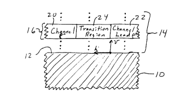
Fig. 1 shows insulating substrate 10 with surface 12 at which TFT 14 is
formed by processes such as deposition and patterned etching of films. TFT
14 includes channel layer 16, and also includes other layers above and below
channel layer 16, as indicated by the ellipses in Fig. 1. Channel layer 16
includes channel 20, channel lead 22, and transition region 24 that includes
the transition between channel 20 and channel lead 22.
Charge carriers in channel 20 have densities of p-, indicating that the
channel is lightly doped or undoped, while charge carriers in the ch~nnel
lead have densities of p +, indicating that the channel lead is heavily doped.
Within transition region 24, densities of charge carriers make a transition
--14--
Attorney Docket No. Dl94027 21~ 0 ~ 0 3
from p - to p + . As illustrated below with various examples, the transition
between a channel and a channel lead can take many forms.
Surface 12 and channel layer 16 extend in a horizontal dimension h, as
indicated, which could be referred to as "horizontal." As illustrated,
positions within transition region 24 can be measured from an origin on
surface 12 at a position aligned with the boundary between ch~nnel lead 22
and transition region 24. Within channel layer 16, transition region 24
extends in horizontal dimension h from ch~nnel lead 22 to channel 20, and
channel 20 then extends further in dimension h. Channel 20 and transition
region 24 each have a first side toward surface 12, which is ordinarily away
from a gate lead, and a second side away from surface 12, ordinarily toward
the gate lead. Channel 20 and transition region 24 extend in ~limen.cion u,
which could be referred to as "vertical," from their first sides to their second
sldes.
Fig. 2 shows insulating substrate 30 with a surface at which TFT 32 is
formed by processes such as deposition and patterned etching of films. TFT
32 includes ch~nnel layer 34, insulating layer 36, and gate layer 38.
Channel layer 34 includes channel 40, channel leads 42 and 44, transition
region 46 including the transition between channel 40 and ch~nnel lead 42,
and transition region 48 including the transition between channel 40 and
channel lead 44. Insulating layer 36 includes insulator 50, electrically
isolating channel layer 34 from gate lead 52 in gate layer 38.
--15--
Attorney Docket No. D,94027 2 1 4 0 4 0 3
-
In TFT 32, gate lead 52 extends alongside channel 40 so that channel 40 can
be switched between its ON and OFF states by changing potential difference
between gate lead 40 and one of channel leads 42 and 44 which is serving as
a source. The other of channel leads 42 and 44 serves as a drain, and the
densities of charge carriers in the transition region adjacent to the drain
result in lower leakage current than would occur if the densities of the
charge carriers in the transition region did not vary in the u dimension.
Fig.3 shows densities of charge carriers in transition region 60, illustrating
how charge carrier densities could vary in the u dimension in any of
transition regions 24, 46, and 48. Transition region 60 is illustratively
shown with a rectangular cross-section having its lower side at the surface of
an insulating substrate and being bounded by a channel at its left and a
channel lead at its right.
Lines 62,64, and 66 illustrate how charge carrier densities vary in the h and
u dimensions within transition region 60. Each of lines 62, 64, and 66
connects positions of equal charge carrier density, with line 62 connecting
positions with a relatively high density, line 64 an intermediate density, and
line 66 a relatively low density. Therefore, charge carrier densities decrease
as distance from the channel lead in the h dimension increases and also
decrease as distance from the substrate in the u dimension increases.
The nearness of lines 62,64, and 66 to each other indicates a relatively steep
gradient of charge carrier densities, separating transition region 60 into two
smaller regions: In the region below line 62, charge carrier densities
Attorney Docket No. D/94027 214 0 4 0 a
approximate p+, a density between that of the channel and that of the
channel -lead; in the region above line 66, charge carrier densities
approximate p -, which can be approximately that of the channel.
Transition regions with charge carrier densities like transition region 60
can be used in a TFT like that shown in Fig. 2 to reduce leakage current.
When channel lead 42 is the drain, transition region 46 acts to reduce
leakage current; when channel lead 44 is the drain, transition region 48 acts
to reduce leakage current. Although Fig. 3 shows a relatively steep gradient
of charge carrier densities in transition region 60, a more gradual gradient
in a transition region should also reduce leakage current.
Charge carrier densities that vary in the v dimension can reduce leakage
current by spreading variations in ch~nnel potential over a larger area,
thereby changing the magnitude and position of the m~ximum electric field.
For example, the charge carrier densities illustrated in Fig. 3 may reduce
the m~ximum electric field and may move it from near the gate lead to a
position nearer the substra-te, possibly near "knee" 70 of lines 62 64, and 66.
Leakage current can be reduced by increasing the distance between the
m?Ximum electric field and the region where the density of charge carriers
is very high in the OFF state condition. In a typical thin-film structure in
which a channel and a gate lead are separated by an insulating layer that is
a dielectric substance, the charge carrier density is very high at the
dielectric-channel interface. Therefore, as the m,qximum electric field
Attorney Docket No. D/94027 2 1~ 0 4 0 3
moves toward ''knee" 70, it moves further from the region of very high
charge carrier density, reducing leakage current.
Fig. 3 thus illustrates an important difference between conventional LDD
techniques and charge carrier densities that vary in the u dimension in a
way that reduces leakage current: In a conventional LDD technique, there
would inevitably be some small, unintentional variation of charge carrier
densities in the u dimension, but there is no evidence that this variation
would reduce leakage current.
C. Simulation
The general features described above have been computer simulated using
numerical simulation techniques ~imil~r to those described and illustrated
in Hack, M., Wu, I-W., King, T.J., and Lewis, A.G., "Analysis of T.e3k~e
Currents in Poly-Silicon Thin Film Transistors," 1993 International
Electron Deuices Meeting Technical Digest, pp. 385-388.
Figs. 4-6 show configurations that were simulated. Fig. 7 is a graph of
m~ximum electric field versus gate voltage, showing simulation results.
Fig. 4 shows a configuration in which gate lead 80 extends alongside
transition region 90, and transition region 90 includes smaller regions 92
and 94. In region 92, charge carrier densities approximate p-, which is that
--18--
Attorney Docket No. D/94027 214 0 4 0 3
,
of the channel. In region 94, charge carrier densities approximate p+,
which is that of the drain to which region 94 connects.
Region 94 is a rectangular region that extends from the drain alongside the
lower side of the channel layer and is approximately half as thick as the
channel layer. Region 92 is a rectangular region that also extends from the
drain, but between region 94 and a gate oxide layer. The configuration of
regions 92 and 94 is referred to as a "bottom only" configuration.
Fig. 6 shows transition region 100, which includes smaller regions 102 and
104. In region 102, charge carrier densities approximate p, which is that
of the channel. In region 104, charge carrier densities approximate p+,
which is that of the drain to which region 104 connects.
Region 104 is a triangular region with a first side facing the drain, a second
side facing an insulating substrate, and a third side or hypotenuse extending
at an angle ~ from the upper end of the first side to a point on the surface of
the insulating substrate where it meets the second side. Region 102 is a
similar triangular region with the same hypotenuse as region 104 and with
its other two sides parallel to the first and second sides of region 104. The
configuration of regions 102 and 104 is referred to as a "grading"
configuration.
Fig. 6 shows transition region 120, which includes smaller regions 122 and
124. In region 122, charge carrier densities approximate p, which is that
--19--
Attorney Docket No. D/94027 214 0 4 0 3
of the channel. In region 124, charge carrier densities approximate p+,
which is that of the drain to which region 124 connects.
Region 124 is a triangular region with a first side &cing the drain, a second
side facing a gate oxide layer, and a third side or hypotenuse exterl~inE from
the lower end of the first side to a point on the surface of the gate oxide layer
where it meets the second side at an angle a. Region 122 is a simil~r
triangular region with the same hypotenuse as region 124 and with its other
two sides para!lel to the first and second sides of region 124. The
configuration of regions 122 and 124 is referred to as a "reverse grading"
configuration.
Fig. 7 shows results of a simulation comparing a standard configuration
without a transition region with the bottom only configuration, the grading
configuration, and the reverse g~ading configuration. In the standard
configuration, a channel e~ctends to the drain, which is uniformly doped.
The simulation assumed a channel layer of 0.1 }lm thick polycrystalline
silicon, a drain to source voltage of 5 volts, a drain uniformly n-doped at a
concentration of 1020 per cm3, and a channel 10 ~lm in length.
In Fig. 7, the vertical axis shows the m~ximum electric field in the h
~limen~ion EX(max) in volts per micron and the horizontal axis shows the gate
to source voltage Vgate in volts. For each configuration simulated, the
simulation obtained EX(max) for Vgate values of ~,--2, and zero volts. In
all cases, EX(max) decreased almost linearly as Vgate went from ~ to zero
--20--
Attorney Docket No. D/94027 214 010 3
volts. The third curve from the top shows the results for the standard
configuration.
The dash-dot line below the standard configuration line shows that, for the
bottom only configuration, E~(maX) is lower than for the shnfl~rd
configuration at all simulated values of Vgate. This suggests that leakage
current would be reduced with the bottom only configuration, because, in
general, leakage current is exponentially dependent on EX(mas)~ being
approximately proportional to [exp (-c/Ex(max))]p~ where p is the density of
charge carriers in the leakage channel and c is an appropriate constant.
The dotted line and solid line fl~nking the dash-dot line show results for the
grading configuration with c~ = 45~ and c~ = 79~ respectively. At other values
of Vgate, for ~ = 45~, EX(max) is higher than for the bottom only configuration,while~ for ~=79~, E~C(ma~c) is lower than for the bottom only configuration.
This suggests that leakage current would be reduced more with a~ = 79~ than
with the bottom only configuration but would be reduced less with ~=45~
than with the bottom only configuration.
The lowest solid line shows results for a grading configuration with c~ = 79~
but with the concentration of n-dopant in the transition region being
2x 1O18 per cm3, significantly lower than the drain doping concentration.
This line suggests that leakage current can be further reduced by doping the
transition region more lightly than the drain.
- Attorney Docket No. D/94027 21~ 0 4 0 3
~.
The dotted line and solid line above the standard configuration line show
results for the reverse grading configuration with ~ = 45~ and ~ = 79~
respectively. As shown, E~maX) is higher for either value of ~ than for the
standard configuration, with ~ = 45~ producing the highest value of EX(mas)~
The simulations also showed that the simulated transition regions in the
bottom only and grading configurations avoid significant increases in gate
overlap capacitance and decreases in drive current. These configurations
also push m~xi mum electric field away from the gate lead. The results of the
simulations suggest that a grading angle of approximately ~ =45~ or more
may be necessary to reduce leakage current.
D. Implementation
The general features described above could be implemented in numerous
ways.
D. 1. High Angle Ion Implantation
The general features described above have been implemented
experimentally by implanting a dopant at a high tilt angle. Fig. 8 shows
acts in producing poly-Si TFTs with transition regions. Fig. 9 shows a cross
section of a first transition region that can be produced by acts in Fig. 8. Fig.
10 shows a cross section of a second transition region that can be produced by
acts in Fig. 8. Fig. 11 shows distributions of leakage current in several
--22--
- Attorney Docket No. D 94027 2 1 ~ O ~ 0 3
poly-Si TFT configurations including two like that in Fig. 9. Fig. 12 shows
TFT leakage as a function of channel width.
The act in box 140 in Fig. 8 deposits a channel film on an insulating
substrate, then performs patterning operations such as etching to produce
device shapes in the channel film layer. The act in box 140 can be
implemented with conventional techniques, and the channel film can be
polycrystalline silicon (poly-Si).
The act in box 142 deposits a gate dielectric layer, which can be an oxide of
the ch~nnel film material. The act in box 144 then deposits a gate material
over the gate dielectric layer and performs patterning operations such as
etching and implantation to produce conductive gate leads a~lJrup.;ately
positioned over portions of the channel film layer. The acts in boxes 142 and
144 can simil~rly be implemented with conventional techniques.
The act in box 146 implants particles of a dopant and a counterdopant to
produce transition regions in areas of the channel film layer under the edges
of the gate leads and conductive channel leads in areas of the channel film
layer that are not covered by gate leads. This act can be implemented in a
number of ways.
The act in box 146 can be implemented by first doping the channel leads
with conventional implantation techniques and by then annealing. Then,
transition regions can be produced in portions of the channel film layer
under the edges of gate leads and adjacent to channel leads that will serve as
- -23--
Attorney Docket No. Dl94027 21 4 0 4 0 3
drains. As described above, charge carrier densities in the transition
regions vary in the u dimension.
Alternatively, the act in box 146 could be implemented by first producing
transition regions and by then producing the ch~nnel leads.
The act in box 146 can produce charge carrier densities that vary in the u
dimension in a transition region by impl~nting both dopant and
counterdopant: The act in box 146 can implant dopant ions at high tilt
angles in the same way that lightly doped drain (LDD) regions are
conventionally formed under gate leads. The act in box 146 can also implant
counterdopant ions at high tilt angles and at lower energies to produce lower
densities of charge carriers close to the gate lead, as illustrated in Fig. 9.
Fig. 9 shows how charge carrier density profiles 190 and 192 combine to
produce transition region 194 with charge carrier densities that vary in two
dimensions. Profile 190 can be produced by implanting dopant ions at high
tilt angles and with energies similar to those used to produce a conventional
LDD region; as a result, the region with a higher charge carrier density p 1 +
is much larger than the region with lower charge carrier density Pl .
Profile 192 can be produced by implanting counterdopant ions at high tilt
angles and at lower energies; as a result, the region with a higher charge
carrier density P2+ is close to the gate oxide and the region with lower
charge carrier density p2-is close to the substrate.
--24--
Attorney Docket No. D/94027
2140403
Charge carrier densities in transition region 194 have a profile that is quite
similar to the "bottom only" configuration described above in relation to Fig.
4. In transition region 194, the charge carrier density will be P3=(pl~2).
Therefore, the region with a higher charge carrier density p3+ iS positioned
away from the gate lead; the region with lower charge carrier density p3-
has approximately the same density as the channel.
The technique described in relation to Fig. 9 has been implemented. Sources
and drains were n-doped with phosphorus ions (P+) at 1X1020 cm-3. A
number of variations were produced on different wafers. In one variation,
referred to as the st~n-l~rd configuration, no further doping of the channel
layer was performed after doping the sources and drains. In a second,
referred to as the LDD configuration, a conventional uniformly doped LDD
region was obtained by implanting P + at an energy of 285 keV at an angle
of 56~ and a dose of 2X1013 cm-2. In a third, referred to as the lightly
counterdoped bottom LDD configuration, a transition region was obtained
by first implanting as a dopant P + at an energy of 285 keV at an angle of 56~
and a dose of 2 X 1013 cm-2, then implanting as a counterdopant boron ions
(B + ) at an energy of 99 keV at an angle of 72~ and a dose of 4x 1012 cm-2.
In a fourth, referred to as the heavily counterdoped bottom LDD
configuration, a transition region was obtained by first implanting P + at an
energy of 285 keV at an angle of 56~ and a dose of 2X1013 cm-2, then
counterdoping by implanting B+ at an energy of 99 keV at an angle of 72~
and a dose of 1 X 1013 cm-2.
--25 --
Attorney Docket No. Di94027 2 1 4 0 4 ~ 3
The implementation included a poly-Si channel layer 0.1 ~m thick deposited
on a glass substrate. An oxide gate dielectric 0.1 ~m thick covered the
channel layer. The dopant and counterdopant ions were implanted at
energies sufficient to penetrate 0.3 ~m beyond the edge of the gate lead. The
implantation to 0.3 llm succeeded in producing an effective transition
reglon.
Table I sllmm~rizes leakage current measurements obtained from the four
configurations described above with VDS = 10 V and with channel width of
50 ~m and channel length of 10 ~m. As can be seen, the median leakage
LEAKAGE CURRENT
DRAIN DOPING PROFILE Median 20%-80%
(pA) Distribution
Standard 9.35 1 6X
LDD (2 x 101 3 cm -2 P + implant) 6.10 1 1 X
Bottom LDD (4 x 101 2 cm -2 B + implant) 3.44 1 1 X
Bottom LDD (1 x 1013 cm-2 B + implant) 1.71 1 2X
TABLE I
current and distribution spread both decreased significantly from the
standard configuration to the LDD configuration, and the median leakage
current further decreased significantly to the two bottom LDD
configurations.
--26--
Attorney Docket No. D/94027
2140403
Fig. 10 shows more fully the distribution of leakage currents for each
configuration in Table I. Fig. 11 shows that leakage current scaled linearly
with channel width for representative configurations, ruling out
contributions due to edge leakage effects.
The implementation results set forth above verify that a transition region in
which charge carrier densities vary in two dimensions can reduce leakage
current more effectively in a TFT transistor than a conventional LDD
configuration. In addition, since the transition region is under the gate, ON
state current in the channel is not sacrificed and OFF state current does not
ncrease.
D.2. Sidewall Spacer and Non-angled Implantation
Figs. 12 and 13 illustrate an alternative technique for implementing the
general features described above. This alternative technique may be
advantageous because it eliminates the need for high angle ion
implantation, which is a nonconventional process. Fig. 12 shows acts in
producing a TFT using the alternative technique. Fig. 13 shows a transition
region produced by the alternative technique.
In Fig. 12, the acts in boxes 210, 212, and 214 are the same as the acts in
boxes 140, 142, and 144 in Fig. 8, except that the dimensions of devices and
gates may be different to allow for sidewall spacers, discussed below.
--27--
Attorney Docket No. D/94027
2140403
The act in box 216 begins the production of transition regions by implanting
a transition region dopant into the channel layer in all areas not covered by
gate leads. This dopant can be implanted with sufficient energy so that the
resulting charge carrier densities are significantly greater in a region near
the insulating substrate than in a region farther from the substrate. The
implantation in box 216 is not at a tilt angle, so that areas under the gates
remain undoped.
The act in box ?18 then produces sidewall spacers so that the transition
regions are covered by gate leads and sidewall spacers. The sidewall spacers
can be formed by conventional techniques using a conductive material such
as doped silicon or silicon germanium. In effect, the sidewall spacers offset
drains from gates, although the drains have not yet been formed.
The act in box 220 produces conductive channel leads in the channel layer,
including both drains and sources, by implanting a dopant at a heavy
concentration in areas not covered by gates and sidewall spacers. This act
can be implemented as in box 146 in Fig.8.
Fig. 13 shows transition region 240, with a doping profile produced by
implanting dopant ions in the act in box 216 after gate 242 has been formed.
After the doping of transition region 240, spacer 244 is formed in the act in
box 218. Then heavy doping is performed by the act in box 220, leaving
channel 246 undoped and transition region 240 with the profile shown, but
making drain 248 conductive.
Attorney Docket No. D194027 214 0 4 0 3
As shown, it is expected that transition region 240 would include two
smaller regions: In one region, charge carrier densities approximate p-,
which is that of channel 246; in the other region, charge carrier densities
approximate p +, a density above that of çh~nnel 246 but not as high as that
of drain 248. The charge carrier densities in transition region 240 are
somewhat similar to the "bottom only" configuration described above in
relation to Fig. 4.
D.3. Variations
The above implementations could be varied in many ways within the scope
of the invention.
The implementations described above include thin film transistors (TFTs),
but the invention might also be implemented in other types of thin-film
structures. In a structure that does not have a channel lead referred to as a
drain, a transition region could be produced adjacent whatever channel lead
functions .simil~rly to a drain. Further, the invention could be implemented
in a modified TFT structure, such as one with a gate below rather than
above the channel layer or with a gate lateral to a channel.
The above implementations employ glass substrates, but other insulating
substrates could be used.
--29--
- Attorney Docket No. D/94027 214 0 4 0 3
.
The above implementations include polycrystalline silicon channels that are
n-conductive, but other thin film materials could be used and p-conductive
channels could be used.
The above implementations use phosphorus and boron dopants, but other
dopants could be used, such as arsenic. Further, it may be possible to
implement the invention with other types of charge carrier sources, such as
an additional lead adjacent to the transition region which can induce charge
into the transition region; the induced charge would fall off in the u
dimension with distance from the lead.
The above implementations use high angle tilt implantation and non-angle
implantation, but other techniques for introducing a dopant could be
applied.
The above implementations are described in terms of particular profiles of
charge carrier densities that vary in two dimensions, but the invention
might be implemented with many other profiles. Further, carrier source
densities in a transition region might range from the defect density,
approximately 10l6 cm~ in poly-Si, up to the ch~nnel lead density.
The above implementations are shown in relation to transition regions that
have a length greater than their thickness, but length and thickness could
be adjusted to whatever dimensions prove optimal. It may be that a
thickness greater than the length may be better in some situations.
--30--
Attorney Docket No. D/94027 21~ 0 4 0 3
The above implementations are described as alternatives to other
techniques such as lightly doped drain (LDD) structures and double diffused
drain (DDD) structures or multiple gate structures. The invention could,
however, be used in combination with LDD, DDD, or multiple gate
structures to obtain improved results.
In the implementations described in relation to Figs. 8 and 12, operations
could to some extent be performed in a different order. For example, the
channel leads could be produced either before or after the transition regions
in Fig. 8.
The above implementations show transition regions with rectangular cross
sections, but transition regions could have any other appropriate shape.
E. Application
The invention could be applied in many ways, including large-area
electronics applications such as active-matri~ liquid-crystal displays and
mage sensors.
F. Miscellaneous
The invention has been described in relation to implementations in which
leakage current is reduced. The invention might also be implemented for
other purposes.
--31--
Attorney Docket No. D194027 214 0 4 0 3
Although the invention has been described in relation to various
implementations, together with modifications, variations, and extensions
thereof, other implementations, modifications, variations, and extensions
are within the scope of the invention. The invention is therefore not limited
by the description contained herein or by the drawings, but only by the
claims.
--32--