Note: Descriptions are shown in the official language in which they were submitted.
WO 94/0266~~L~4~0 P~/US93/0695~ '
SEMIMETAI~SEMICONDUCl`OR ¦HETEROSTRUCTURES AND MlJLTlLbYERS
Field of the InventiQn
The invention relates to the fabrication of semimetal/semiconductor
heterostructures. In particular, the inventiorl relates to the fabrication of
one or more combinations of semimetal and semiconductor layers having
compatible crystal symmetry across each heterojunction between a given
semimetal and the adjoining semiconductor. Any of the semimetal layers ~`
sandwiched between semiconductor layers may be grown thin enough that
the semimetal layer becomes a semiconductor.
Background of the Invention
The incorporation of metallic films embedded in a semiconductor
device, thereby creating a hybrid structure, has received significant
attention. This has primarily been motivated for two reasons: (i) because
16 of the low resistivity of the metals that would enable fabrication of buried
contacts, interconnects and ground planes, which are considered esser.tial
to the three dimensional integration of semiconductor devices; and (ii)
because of the possibility of combining the transport properties of metals
and semiconductors to create novel or improved device applications, for
example metal base transistors or high frequency switches.
Synthesis of metal/semiconductor hybrid structures impose
stringent requirements on the film and heterojunction properties.
Specifically, the crystalline quality and thermal stability of both the
embedded metallic layer and the semiconductor overgrowth, as well as the
integrity of the heterointerfaces, are of paramount importance. While the
epitaxial growth of metals on semiconductors is now relatively routine
with low temperature growth techniques such as molecular beam epitaxy,
for example epitaxial metallization systems reported to be grown on GaAs
are Al, Ag, Fe, and body-centered-cubic Co asnong others, see A. Y. Cho
and P.D. Dernier, J. A~pl. Phys., 49.3328 (1978); J. Massies, P. Delescluse,
WO 94/02665 PCI /US93/06955 -
345Q
P. Etienne and N~T. Linh, Thin Solid F~lms, 90, 113 (1980); J.R. Waldrop l,
and R.W. Grant, A~pl. Phys. Lett., 34, 630 (1979); G.A. Prinz and J.J.
Krebs, Appl. Phys. Lett., 39.397 (1981); and G.A. Prinz, Phys. Rev. Lett.,
54, 10~1 (1985) which are incorporated herein by reference, it is noted
6 that these metal/semiconductors heterostructures are not
thermodynamically stable since the metals will react with As and/or Ga
to form metal-As (M-As) and metal-Ga (M-Ga) compounds. In addition,
the Al-containing compounds are susceptible to an Al/Ga e~change
reaction at elevated temperatures. A much more serious limitation has
been the inability to grow high quality single crystal semiconductor ~llms
on deposited metal layers. -
Key factors for consideration in fabricating hybrid structures have `
involved the differences in crystal structure, thermal stability, bonding
disparities, snd growth compatibility of the constituent materials. While
such factors have seriously hindered the fabrication of buried metal
structures, the growth of a semiconductor on metal (NiAl/GaAs~ has been
reported. See T. Sands, A~pl. Phys. Lett., 57, 197 (1988), and ~.P.
Harbison, T. Sands, N. Tabatabaie, W.K. Chan, L.T. Florez, and V.G.
Keramidas, A~pl~ Phys. Lett., 53, 1717 (1988) which are incorporated
herein by reference. However, fabrication of only a single
semiconductor/metal layer has been achieved. An alternative approach
has involved incorporating a semimetal, rather than a conventional metal,
into the heterostructure. Recently, ErAs has been successfully grown on
GaAs and shown to exhibit semimetallic behavior. See C.J. Pairnstrom,
N. Tabatabaie, and S.J. Allen, Jr.,A,ppl. Phys. Lett., 53, 2608 (1988), which
is incorporated herein b~ reference. Unfortunately, the resistivity of this
structure was measured to be 7.2 mQ cm--nearly four orders of magnitude
higher than the resistivity of copper, and like the prior art NiAl/GaAs
structure, only a single layer has been successfully incorporated into a
heterostructure. In addition, these prior art systems have inherent
problems associated with materials incompatibilities, and differing crystal
structures that will continue to plague the performance of electronic
WO 94/02665 PCr/US93/06955
4JS0
devices fabricated with these structures. Put simply, none of the prior art `.
metaVsemiconductor or semimetal/semiconductor structures that have
been fabricated have achieved optimal heterostructure properties required
of potential applications for these structures. ~.
The present invention enables the fabrication of stable, high quality
semimetal/semiconductorinterfacesandmultiplesemimetal/semiconductor
layers. In addition, the present invention enables semimetal layers in a
semimetal/semiconductor multilayer to be fabricated such that the
semimetal becomes a semiconductor. The semimetal/semiconductor
heterostructures of the present invention are believed to have applications
in microelectronics devices, especially high speed microelectronics, optical
devices, mesoscopic physics, and potentially high-temperature
superconductivity.
Summarv of the Invention
The present iIlvention provides novel and useful semimetal/
semiconductor heterostructures and multilayers. In accordance with the
present invention, stable, high quality semimetal-semiconductor interfaces
can be fabricated by exploiting a compatible crystal symmetry across the
heterojunction between a semimetal and a semiconductor.
The semimetal/semiconductor heterostructures are fabricated by
growirlg a rhombohedral semimetal in a [111] direction on a substrate
material having a (111) orientation, and then growing a zincblende
semiconductor in a [111] direction on the rhombohedral semimetal.
Suitable rhombohedral semimetals include Bi~Sb,.", or As, while suitable
zincblende semiconductors include In,~Gal.~Sb, In,~Ga,.~As, Al~Gal.~As, or
Al~Gal,~Sb, where x ranges from zero to one~ The substrate material can
comprise numerous materials including, but not limited to In~Ga,.
,~Sb, In~Ga, ~As, Al"Gal.~As, Al~Ga~.~Sb, or A1203~
Unfike the prior art, the present invention enables multiple
semimetaVsemiconductor layers to be fabricated. A single layer
semimetal~'semiconductor heterostructure, comprising a rhombohedral
wo 94f0266~ )45~ PCl/US93/069~5 - :
semimetal grown in a [111] direction on a substrate and a zincblende
semiconductor grown in a [111~ direction on the semimetal, is utilized in ~;
effect as the base of the semimetal/semiconductor multilayer structure. ' ~ j
Alternating layers of rhombohedral semimetal, grown in a ~111] on the
preceding semiconductor layer grown, and zincblende semiconductor,
grown in a [lllJ direction on the preceding semimetal layer grown, are
then fabricated on the base. The number of semimetal/semiconductor
layers grown is dependent on the application of the
semimetal/semiconductor multilayer structure.
The semimetaVsemiconductor heterostructures and multilayer
structures may be grown by any low temperature epita~ial growth process.
Suitable low temperature epitaxial growth processes include molecular
beam epita~y, chemical beam epitaxy, and metal organic chemical beam ~`
epita~
The respective semimetal and semiconductor layers are grown to a -
thickness which is dependent on the particular application of the
semimetal/semiconductor heterostructures or multilayer structures.
However, the lsyers will typically have a thickness in the range of 10- `
500~.
If fabricated in accordance with conventional techniques, the
semimetal layers of the semimetal/semiconductor structures of the present
invention will likely be fabricated with thicknesses greater than
approximately 100~ such that the semimetal has a low resistivity like
metals. Such low resistivity semimetal layers in the
semimetaUsemiconductor structures may find applications as buried
contacts, interconnects and ground planes. Such applications were
previously envisioned primarily formetal/semiconductor hybrid structures~
The inventors have also discovered that if a semimetal layer in a `
semimetal/semiconductor multilayer structure of the present invention is
sandwiche~d between semiconductor layers and is fabricated thin enough,
then the semimetal becomes a semiconductor. The thickness L~ of the
semimetal must be comparable to or less than the de Broglie wavelength
WO 94/0266~ PCI /l,'S93/0695~ `
of the carriers. In general, the thickness L~ must be less than 100A.
The semimetal/semiconductor heterostructures and multilayer ~
structures are believed to have been useful applications in: microelectronic -j
devices, especially high speed microelectronics, optical devices, mesoscopic j'
physics, and high-temperature superconductivity.
Brief Description of the Drawin~s
A better understanding of the present invention can be obtained
when the following detailed description is read in conjunction with the
following drawings in which: ;
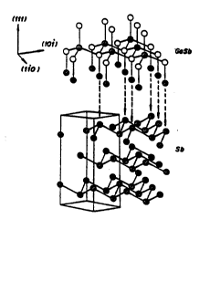
Figure 1 is a perspective view illustrating compatible crystal
symmetry across the heterojunction between rhombohedral semimetal and -
zincblende semiconductor crystals in accordance with the present `~
invention;
Figure 2 is a side view of a single layer semimetal/semiconductor
heterostructure in accordance with the present invention;
Figure 3 is a side view of a multilayer semimetal/semiconductor
swcture in accordance with the present invention;
Figure 4a is a diagram of energy versus wavenumber (k) for Bi or
Sb [Bi, Sb] i~ bulk form; and
Figure 4b is a diagram of energy versus wavenumber (k) for Bi or
Sb ~Bi, Sb] confined in a quantum well.
Detailed Descri~tion of the Invention
A. Introduction. Recent developments by the inventors now
enable, for the first time, the fabrication of stable, high quality semimetal-
æemiconductor interfaces and multilayers consisting ofthe zincblende III-V
semiconductor family (for example GaSb, InAs, AlSb, GaAs, InP) and the
semimetals that have a rhombohedral crystal structure (for example Sb,
Bi and As, and associated alloys). See T.D. Golding, H.D. Shih, J.T.
Zboror~,vski, W.C. Fan, P.C. Chow, A. Viglia~te, B.C. Covington, A. Chi,
J.M. Anthony and H.F. Schaake, Accepted for publication, J.Vac. Sci.
w094/0266~ O~ ~ PC~/US93/0695~ ~
..
Tech., and T.D Golding, J.A. Dura, W.C. Wang, J.T. Zborowski, A.
Viliante, and J.H. Miller, Jr., "Investigation of Sb/GaSb Multilayer
Structures for Potential Application as a Narrow Bandgap System,"
Accepted forpresentat:ion at the International Conference on Narrow-Gap
5 Semiconductors, Uni~ersity of Southhampton, U.K, 19-23 July 1992 which
are incorporated herein by reference. The semimetal layers have been
found to have extremely low room temperature resistivities, significantly
lower than that of copper. See T.D. Golding, J.A. Dura, W.C. Wang, J.T
Zborowski, A. ~iliante, and J.H. Miller, Jr., "Investigation of Sb/GaSb
Multilayer Structures for Potential Application as a Narrow Bandgap
System," Accepted for presentation at the International Conference on
Narrow-Gap Semiconductors, University of Southhampton, U.K, 19-23
July 1992. The present invention overcomes the limitation of prior art
investigations and concepts and also significantly extends the range of
applications that have been able to be envisioned in the conventional
metal/semiconductor hybrid structures.
The present invention overcomes the disparity in crystal structure
of semimetal and semiconductor materials by utilizing a common crystal
symmetry across the heterojunction of rhombohedral semimetal and
zincblende semiconductor crystals. This results in the ability to grow
semimetals on semiconductors and reciprocal structures with exact
regist~ of the two lattices across the interface. This permits, therefore,
the fabrication of very high quality heterointerfaces without dislocations,
and dangling bonds, for example.
The semimetal layers in the semimetal/semiconductor structures
fabricated by conventional techniques have similar conductivities to
metals. In addition, the semimetals unlike metals, may be converted into
semiconductors using quantum size effects. During the fabrication of the
semimetallsemiconductor structures, the thickness of the semimetal layers
may affect whether the semimetal layer is converted into a semiconductor.
B. Description. The difficulty in the prior art with fabricating
hybrid heterostructures has involved the disparit y in the crystal structures
WO 94J02S65 PCI /US93/0695~ `
5~)
of the constituent materials which prevent the formation of high quality,
defect free heterojunctions. However, it has been known in the prior art
that when, on specifilcally chosen grown planes, two crystal structures
have a compatible surface lattice they can be exploited for heteroepitaxial
growth. The surface registry can occur either in a supercell, or when the
naturally occurring primary surface unit cell of two different crystal
structures is identical (to within only a small mismatch in lattice
constants). See A. Zur and T.C. McGill, J. A~pl. Phys., 55, 378 (1984),
and J.E. Cunningham, J~. dura and C.P. Flynn, in Metallic Multilayer
and Epitaxy, ed. by M. Hong, S. Wolf and D.C. Gubser, Me~allurgical
Society Inc. (1987) which are incorporated herein by reference. It is this
latter form of matching which the present invention exploits to create a
new group of semimetal/semiconductor structures.
It has been discovered that single layer and multilayer
semimetaVsemiconductor structures can be fabricated with rhombohedral
semimetals having a (111) orientation and zincblende semiconductors
having a (111) orientation. Suitable rhombohedral semimetals include
Bi~Sbl,~ or As, while suitable zincblende semiconductors include
Ir~Gal ~Sb, In~Ga~.~As, Al~Gal ~As, or Al~Ga,.~Sb, where x ranges from zero
to one.
The followiIlg discussion relates to the fabrication of a GaSb/Sb
semiconductor/semimetal heterostructure, however the discussion is also
relevant to fabrication of other rhombohedral semimetal/zincblende
semiconductor structures. The bulk structure of Sb is rhombohedral
(trigonal) lattice parameter a = 4.506~ and = 57.11, see Elements of
X-ray Diffraction, B.C. Cullity, Addison-Wesley which is incorporated
herein by reference, while GaSb is zincblende with a = 6.096~. The (111)
plane of Sb forms a hexagonal net which is structurally nearly identical
to that of~GaSb in its (111) plane. The in-plane interatomic distance in
Sb and GaSb is 4.308~ and 4.310~, respectively, resulting in a (111)
planar mismatch, /~aj/ai, of only 0.0006 (at 273 K). Therefore, formation
of defect free, strainless interfaces are a possibility with this system if
wo 94/0266~ L~ r~(~) Pcr/us93/069s~
grown on the ~111) orientation. In ad~ition, the coefficients of linear
e~pansion of Sb and GaSb are comparable (aGaSb = 6.9 x 10⁶, aSb = 9
x 10~) and potential cross doping effects which have been of concern in t
some of the prior art mixed semimetal/semiconductor combinations are
eliminated because Sb is common in Sb/GaSb structures. Figure 1
illustrates compatible crystal symmetry across the heterojunction between
the zincblende semiconductor crystal GaSb and the rhombohedral
semimetal crystal Sb.
The semiconductor/semimetal structures can be grown by any low
temperature epitaxial growth process. In order to ensure that the
common crystal symmetry is exploited the semimetal and semiconductor
layers must be grown along the [111] direction, and this necessitates
growth on a (111) oriented substrate or template that has an atomic
surface structure that is six fold symmetric. Suitable substrates include,
but are not limited to In,~Gal.~Sb, In~Gal~As, Al~Gal~As, or ALGal."~Sb.
Specific examples of suitable substrates are InAs(111), GaSb(111),
GaAs(111) or sapphire(111) (A1203~. In general, to fabricate a single layer
semimetaVsemiconductor heterostructure 20 (see Figure 2), a
rhombohedral semimetal 22 is grown in a [111] direction on substrate 24
having a ~111) orientation. A zincblende semiconductor 26 is then grown
in a ~111] direction on semimetal 22.
The following is a more detailed description of the fabrication of a
semimetal/semiconductor structure. Although the discu~ssion is limited to
a Sb/GaSb structure, it is equally applicable tO the range of rhombohedral
2~ semimetals, and the zincblende semiconductor materials pre~nously
mentioned.
The Sb semimetal and GaSb semiconductor films are grown by
molecular bearn epita2y (MBE) in a commercial (Riber 32) growth
chamber, using a standard Sb effusion cell producing Sb~, and a standard
liquid-metal Ga source. See "Molecular Beam Epitaxy" Ed. M.a. Herman
and H. Sitter, Springer-Verlag (1989) which is incorporated herein by
reference; see also T.D. Golding, J.A. Dura~ W.C. Wang, J.T. Zborowski, -
WO94/02665 2~ -r~{~ PCI/US93/069
A. Viliante, and J.H. Miller, Jr., "Investigation of Sb/GaSb Multilayer
Structures for Potential Application as a Narrow Bandgap System,"
Accepted for presentation at the International Conference on Narrow-Gap
Semiconductors, Universit;y of Southhampton, U.K, 19-23 July 1992.
Other growth techniques besides MBE, such as chemical beam epita~y,
and metal organic chemical beam epitaxy are equally suitable. The
substrates employed are GaSb(111)A and (111)B oriented, and are indium-
bonded to Molybdenum blocks. Homoepitaxial GaSb buffer layers of
approximately 0.B~m may be grown prior to epilayer or multilayer growth,
although this is not essential. Molecular fluxes are determined from
- ~ measurements by an ion gauge interposed in the beam path. Substrate
temperatures above 425C are measured by an optical pyrometer, and
below 425C are estimatedby extrapolatingreadings from a thermocouple
mounted behind the sa,mple block. Growth is monitored by in-situ
15 ~ reflection high energy electron diffraction (RHEED). Growth rates for Sb
are~ calibrated by Rutherfort backscattering spectromet~ (RBS), and
- gr:wth rates for GaSb by RHEED intensity oscillations and RBS.
Epitaxial grown of Sb on both GaSb (111)A and (111)B is achieved
- ~ by increasing the Sb residence lifetime on the GaSb surface by lowering
the temperature below a nucleation temperature, Tn(JSb), which is
independent of the growth orientation. For Jsb = 7x10⁷ torr, Tn is equal
to 260C for epitaxial growth of Sb on GaSb. For epitaxy on both GaSb
(111)A and (111)B, initial growth is slow and simultaneous diffraction
; from;epitaxial Sb and GaSb is observed by reflection high energy electron
26 diffraction (RHEED). A streaked, well defined (1x1) RHEED pattern,
-~ showing single phase, two dimensional growth results after surface
coverage is complete. It is noted that v~rith nearly identical surface nets,
the ~111) Sb is distinguishable from (111)A or (111)B GaSb only by the
RHEED~surface reconstructions. At Tnt and with the flux ratios Jsb z
...
1.1, the surface reconstructions for GaSb(111)A and (111)B are 5x2 and
&8, respectively. Unlike GaSb, the Sb surface has inversion symmet~
.
4~345~)
WO g4/~)266~ PCI/US93/06955 _
~,:
! ' l ' ;
about the 111 plane and has a 1x1 reconstruction regardless of whether
grown on Gasb (111)A or (111)B. Epitaxial growth, once established, may
be continued to appro~imately 200 C. Below this temperature, diffraction
rings indicative of polycrystalline grown are observed. -
It is noted that with Sb flux constantly present on the GaSb
surface, slow initial growth, where surface accommodation and desorption
are only slightly unbalanced, is a critical condition for epitaxy. For
example, if the surface concentration of Sb is increased rapidly~ by cooling
quickly through Tn~ multiply oriented, three-dimensional growth occurs.
However, and most importantly, Sb may be successfully nucleated below j`
Tn if the GaSb surface is not exposed to a Sb flux for a period of several
seconds.
After deposition of the Sb layer to the required thickness, GaSb can
be grown epitaxially on top of the Sb layer by standard MBE growth
techniques, and the fabrication of a single layer semimetallsemiconductor
heterostructure is complete. To fabricate a multilayer -
semimetaVsemiconductor structure, another Sb layer may be grown on top
of the just grown GaSb layer by the technique described above, and then `-
another GaSb layer may be grown by standard MBE growth techniques
on the just grown Sb layer. This pattern is repeated until the desired
number of alternating semimetal and semiconductor layers have been
fabricated.
A schematic of a generic semimetaVsemiconductor multilayer `
structure 30 is shown in Figure 3. Figure 3 illustrates substrate 24 and `
2~ multiple semimetal layers 22 and semiconductor layers 26. The number
of semimetal/semiconductor layers is dependent on the device or device
characteristics required. It is also noted that the semimetal/semiconductor
combinations employed in the semimetal~semiconductor structure are ,
dependent on device characteristics desired, but are restricted to those `
combinations with close lattice match, such as GaSb/Sb. The layer
thicknesses for each semimetal layer (L",) and each semiconductor layer
(L,) is also dependent on the device characteristics required and speci~lc
- wo 94/0266~ X~L~ Pcr/us93/o69
~ ~.
materials employed, but Lm and ~, will typically have values in the range
10-500~. When the semimetal layers have a thickness greater than about
100~, they have resistivities comparable to metals. As will be discussed
in more detail below, such low resistivity layers may find applications as
buried contacts, interconnects and ground planes. Such applications were
previously envisioned primarily for metaVsemiconductor hybrid structures.
As will be discussed below, the thickness Lm for a semimetal sandwiched
between semiconductor layers may be made thin enough, in accordance
with the quantum size effect, that the semimetal becomes a
semiconductor.
The quantum size effect is generally defined as a dependence of the
thermodynamic properties and kinetic coef~lcients of a solid on its
characteristic geometric dimensions when the latter becomes comparable
to or less than the de Broglie wavelength of the charge carriers. When
the thickness of the solid (L,~) is comparable to or less than the de Broglie
wavelength of the solid's carriers, quantization of the carrier motion
occurs.
In the absence of quantum confinement As, Sb, Bi, or Bi~Sb~, are
semimetals. For these materials the conduction band minimum (3-fold
; 20 degenerate at the ~point) lies at a lower energy than the valence band
maximum (6-fold at the H-point in Sb, 1-fold at the T-point in Bi). The
overlap of the two bands is ~ 180 meV in Sb and ~ 40 meV in Bi. If the
semimetaI layers are spacially confined by sandwiching the semimetal film
between layers of a suitable barrier material, such as GaSb, AlSb or InAs,
then by decreasing the thickness of each semimetal layer, the conduction
band will move up in energy, while the valence band will move down~ See
Figurei 4a for a diagram of energy versus wavenumber (k) for Bi or Sb ~Bi,
Sb] in bulk form, and Figure 4b for a diagram of energy versus
wavenumber (k) for Bi or Sb [Bi, Sb] confined in a quantum well. In the
multilayer semimetaVsemiconductor structures described above,
semiconductor layers 26 sandwiching semimetal layers 32 are suitable
barrier material. See Figure 3. Using appropriate effective masses, see
WO 94/02665 PCl /US93/0695S
J.P. Issi, Aust. J. Phys., 32, 585 (1979) which is incorporated herein by
reference, the two bands should cross at L~z100~, where L~ and Ly may be
much greater than Lz, at which point the semimetal becomes an indirect
narrow-gap semiconductor. In general, the thickness below which the two
bands cross will depend inversely on the square root of the band overlap,
with 100~ being the calculated value for Sb. If the barrier materials are
the semiconductors in a semimetal/semiconductor multilayer and are thin
enough that there is coupling between adjacent semiconductor layers, the
entire semimetaVsemiconductor multilayer becomes an indirect narrow-
gap superlattice. Like naturaily-occurring and man-made semiconductors,
the indirect gap of the semiconductors converted from semimetals can
have a value between zero to æeveral hundred meV. The indirect gap
dependis on the thickness of the semiconductor layer converted from a
semimetal, and the types of barrier materials used.
C. A~lications.
1. Hi~eh speed microelectronics. Fabrication of low resistance
contacts and metallic interconnects is extremely important for high speed
microelectronics. The ability to fabricate buried metal structures in
semiconductors is expected to lead to many new devices. For example,
such metallization schemes show promise for the fabrication of metal base
transistors, such as the permeable base transistor (PBT), and resonant
tunneling triodes. Metal base transistors are the fastest known three-
terminal semiconductor devices, with upper cutoff frequencies above 200
GHz having been achieved in GaAs PBTs. See M~. Hollis, K.B. Nichols,
R~. Murphy, R.P. Gale, S. Rabe, W.J. Piacenti, C.O. Bozler and P.M.
Smith, IEDM Tech. Diges~, 102 (1985) which is incorporated herein by
reference.
The observation of a resonant tunneling component, showing
negative differential resistance, in the axial current-voltage characteristics
of MB~grown AlAs/NiA1/AlAs double-barrier structures has been
reported. See N. Tabatabaie, T. Sands, J.P. Harbison, H.L. Gilchrist, and
V.G. Keramidas, Appl. Phys. Lett., 53, 2528 (1988) which is incorporated
WO 94/02665 ~ 't, ~ PCrtUS93/06955
~ 3
herein by reference. This phenomenon is an indication of quantum
confinement in the thin NiA1 film, and is the first direct observation of
two-dimensional electron subband formation in metals. Technologically,
this demonstration of resonant conduction through metal quantum wells
is an important step towards the fabrication of resonant tunneling
resistance, with expected operating frequencies in the THz range.
Integration of such a device into semiconductor technology could find
applications in the ares of high speed digital circuits, frequency
multipliers, and tunable oscillators/amplifiers.
~3ystem applications in communications, radar and other areas have
stimulated those skilled in the art to attempt to increase the frequencies
of operation and improve the noise figures of metal-semiconductor field-
effect transistors (MESFETs). The development of a high qualit~ metal-
semiconductor Schottky barrier interface is crucial to achieving high
performance in these devices. Recently, the fabrication of an all-epitaxial
- semimetal-semiconductor Schottky diode has been reported. See J.W.
Sulhoff, J.L. Zyskind, C.A. Burrus, R.D. Feldman, and R.F. Austin, Appl.
Phys. Lett~.? 56~ 388 (1990) which is incorporated herein by reference.
The semimetal layers in the semimetaVsemiconductor structures of
the present invention may be fabricated with low resistivities like metals.
It is expected that the single and multilayer semimetaVsemiconductor
structures of the present invention will be viable alternatives to
metaVsemiconductor structures. Furthermore, as discussed above, at
present, metal/semiconductor structures are not thermodynamically stable.
In addition, currently there is an inability to grow high quality single
crystal semiconductor layers on deposited metal layers.
An additional potential benefit of semimetal/semiconductor
heterostructures relates to the fact that high carrier concentrations
already e~Eist in the semimetal, without the need to introduce high
concentra~ions of donor or acceptor dopants which increase impurity
scattering. As a consequence, semimetal films can advantageously replace
thin, degenerately doped semiconductor films in numerous devices, such
WO 94/0266~ ~L~ 0 PCI/US93/0695~ --
as the modulation-doped field effect transistor (MODFET), for example.
In addition, a large shift in the Fermi level for a sufficiently thin
semimetal layer, arising from quantum size effects, see M.L. Huberman
and J. Maserjian, Phys. Rev., B37, 9065 (1988) which is incorporated
6 herein by reference, suggests that such a semimetal layer would behave
as a highly concentrated dopant sheet, which could be incorporated into
modulation doped structures. The dopant type is donor or acceptor,
depending on whether the semimetal is n-type or p-type, respectively.
In summary, semimetal/semiconductor heterostructures could
potentially be utilized for numerous mîcroelectronic device applications.
2. Optical detectors. -
':
Quantum-size effects have been calculated in thin layered
semiconductor-metal-semiconductor heterostructures using an ideal free-
electron model for the metal layer. See M.L. Huberman and J. MaseIjian,
Phys. Rev., B37, 9065 (1988) which is incorporated herein by reference.
Optical transitions between quantized subbands are allowed in the metal
layer. The possibility of such intersubband transitions suggest
optoelectronic applications. At electric fields sufficient to block the
conduction normal to the layers, electrons photoexcited into higher
quantum states can escape by tunneling through the top of the barrier,
producing a photocurrent. Optical detection by intersubband absorption
may then be possible in such quantum well structures.
An alternative optical device is a semiconductor/semimetal Schottky
(S3) photodiode. Recently, high quantum efficiencies, in the range of 12%,
have been achieved for an HgCdTe all-epitaxial S3 photodiode, despite the
fact that the device was not optimized for layer thicknesses, carrier
concentrations, passivation and other device characteristics. See J.W.
Sulhoff, J.L. Zyskind, C.A. Burrus, R.D. Feldman, and R.F. Austin, A~pl.
Phys. Let~., 56, 388 (1990) which is incorporated herein by reference.
Such photovoltaic detectors are of interest for applications in optical
communications and for focal plane alTays. The difficulties of forming p-n
junctions in Hgl.sCD,~TE by impurity doping are avoided in the S3
wo 94/02665 PCr/US93/06955 -
3 L~ Q
~ 5
photovoltaic detector. In accordance with the present invention, it may
be possible to fabricate S3 photodiodes for operation over a broad
wavelength range of interest for focal plane arrays if the operating
temperature is reduced. With such an all-epitaxial structure, functional .
layers could be stacked to make integrated structures with more
sophisticated capabilities. See also U.S. Patent Application Serial No.
, by T. Golding et al., entitled "Optical Switches and
Detectors Utilizing Indirect Narrow-Gap Superlattice Materials, filed
concurrently herewith, which is incorporated herein by reference.
3. Mesoscopic ~hysics.
New quantum-well structures can be achieved by sandwiching thin
metal layers between two semiconductors. Two-dimensional electron gas
(2DEG) phenomena, which previously was considered restricted to
semiconductors, is observable in metals. Since the metal Fermi energy
always lies in the semiconductor band gap, the electrons in the metal at
the Fermi energy are confined. Consequently, the normal wave-vector
component of the electron states as the Fermi surface is quantized. `
The epitaxial Sb/GaSb layered structures of the present invention
are ideally suited for studies in the mesoscopic regime, AF < ~ L ~ < L~.
where AF is the Fermi wavelength, L is a typical lateral device dimension,
and L. is the phase coherence length, which is determined primarily by
the inelastic diffusion length. The use of epitaxial Sb in mesoscopic
structures is advantageous, both because the carrier concentration is
substantially higher, and, consequently, AF is smaller, than that attainable
2~ in a typical 2DEG in a semiconductor heterostructure, and also because
the inelastic diffusion length is longer than in conventional metals, such
as gold. Phenomena which can be investigated ~nth mesoscopic structures
include, but are not limited to, universal conductance fluctuations,
persistent~currents in normal metal rings, ballistic electron optics in two-
dimensional electron systems, single electron double barrier resonant
tunneling through quantum dots, and electron transport through an
"antidot" array.
WO 94/02665 f'~ 50 PCI /US93/06955
: ., ` . ` ':`
i ~
4. Collective electrical transport phenomena.
An excitingpossibility is the prospect of observingphase transitions
to ground states exhibiting collective electrical transport phenomena,
including charge-density-waves (CDWs), antiferromagnetism, and novel
mechanisms of superconductivity. One such novel mechanism includes the
exciton pairing mechanism, proposed by Ginzburg, Bardeen and other
investigators, see W~. Little, Phys. Rev., 134, A1416 (1964); V.L.
Ginzburg, Usp. Fiz. Nauk, 101, 185 (1970). ~Sou. Phys. - Usp., 13, 335
(1970)3; and D. Allender, J. Bray, and J. Bardeen, Phys. Rev., B7, 1020
(1973) which are incorporated herein by reference, which has been
predicted to cause superconductivity with high transition temperatures in
suitable thin metallic f~ms in intimate contact with narrow bandgap
semiconductors and in suitably designed metal-semiconductor
superlattices. More recently, a number of investigators, see C.M. Varma,
P.B. I.ittlewood~ S. Schmidt-Rink, E. Abrahams, and A.E. Ruckenstein,
Phys. Reu. Lett., 63, 1996 (1989), and A. Virosztek and J. Ruvalds, Phys.
Reu. Lett., 67, 1657 (1991) which are incorporated herein by reference,
have invoked the e~citon mechanism in order to explain high temperature
superconductivity in the layered cuprates, and the small isotope shift in
Tc, and recent experiments, see I. Bozovic, Phys. Rev., B~, 1969 (1990),
I. Bozovic, J.H. Kim, J.S. Harris, Jr. and W.Y. Lee, Phys. Reu., B43, 1169
(1991), and J. H. Kim, I. Bozovic, C.B. Eom, T.H. Geballe and J.S. Harris,
Jr., Physica, C174, 435 (1991) which are incorporated herein by reference,
probing the comple~ dielectric functions of cuprate superconductors
provide compelling evidence that virtual electronic excitations indeed play
a major role in mediating the pairing in cuprate high Tc superconductors.
The inventors have observed, in two GaSb/Sb multilayer samples
fabricated in accordance with the present invention, hysteretic resistive
anomalies~ indicative of a first order phase transition, such as the CDW
and commensurability locking transitions observed in 1T-TaS2, see J.P.
Tidman and R.F. Frindt, Can. J. Phys., 54, 2306 (1976), F.J. DiSalva and
J.E. Graebner, Solid State Commun., 2~, 825 (1977), and R.V. Coleman,
wo 94/0266~ ~() PCr/US93/û695~ -
1 ~ :
B. Drake, P.K. Hansma and G. Slough, Phys. ~ev. Le~t., 55, 394 (1985) - `-~
which are incorporated herein by reference, and other quasi-two
dimensional metals. In a thin film semimetal, such as Sb, with proper
choice of the orientation of the thin film, the two-dimensional Fermi r~
surfaces of electrons and holes can be configured to be of approximately
equal shape, i.e. Ec(p) = Eh(p~Q) (nesting condition). Here, Ee (Eh) is the
electron (hole) energy dispersion and Q is the distance in momentum
space between the extreme of these two bands. Under this situation, the
system will be unstable with respect to the formation of interband electron
and hole pairs, and it will undergo a CDW transition. See A.I. Rusinov,
Do Chan Kat and Yu V. K~paev, Sov. Phys. JETP, 38, 991 (1974) which -
is incorporated herein by reference. This transition in turn induces a E ~
singularity near the bottom of the conduction band and top of the hole
band. When the intraband electrons (holes) form Cooper pairs, either due
to phonons, excitons, or two-dimensional acoustic plasmons, the
superconductingtransition temperature maybe significantly enhanced due
to the singularity in the density of states. It is expected that there will be
an interplay between CDW formation and superconductivity.
The foregoing disclosure and description of the invention are
illustrated and explanatory of the preferred embodiments, and changes in
the dimension, materials, and fabrication may be made without departing
from the spirit of the invention.
What is claimed is: