Note: Descriptions are shown in the official language in which they were submitted.
W094/28656 2 1 4 0 8 51 PCT~S94/05837
TRANSMITTING AND RECEIVING APPARATUS AND METHOD
INCLUDING PUNCTURED CONVOLUTIONAL ENCODING AND DECODING
Field of Invention
The present invention relates generally to feed
forward error correction transmitters, receivers, systems
and methods employing punctured convolutional encoding
and decoding and more particularly to such transmitters,
receivers, systems and methods wherein (a) a serial bit
stream at the transmitter and/or receiver is divided into
a pair of bit streams and/or (b) feed forward error
correction data signals having 2/3 and 6/7 punctured
codes are radiated at mutually exclusive times from a
geosynchronous satellite at first and second power
levels, respectively, to a terrestrial receiving site
including an antenna dish having a diameter of no more
than approximately one meter.
sackqround Art
In a convolutional encoded feed forward error
correction transmitter, a binary bit stream is divided
into first and second bit streams respectively including
sequential bits Pl(0), P1(1), P1(2), 1( )
2 2( )~ P2(2), P2(3), P2(4) etc. In one-half
rate convolutional encoding, the first and second bit
streams are formed by combining adjacent bits in the
original bit stream in accordance with a modulo 2
function, i.e., by using half adders responsive to the
adjacent bits.
Because of the redundancy in the first and second
bit streams, it is possible to remove some of the bits
from these bit streams without substantial loss of
W094/28656 PCT~S94/05837 _
40~S ~ 2
information; such removal of bits from the first and
second bit streams is generally referred to in the art as
puncturing. Optimum puncturing codes for these bit
streams are disclosed by Yasuda et al., "Development of
Variable-Rate Viterbi Decoder and its Performance
Characteristics," 6th International Conference on Digital
Satellite Communications, Phoenix, Arizona, September
1983. Yasuda et al. discloses optimal puncturing rates
from 2/3 to 16/17. The 2/3 puncturing code or rate is
represented by:
Table I
11
Lines 1 and 2 of Table I respectively indicate
puncturing operations performed on the bits of the first
and second bit streams. The first place in line 1
indicates the puncturing operations to be performed on
bits P1(0), Pl(2), Pl(4) etc. of the first bit stream;
the second place in line 1 indicates puncturing
operations performed on bits P1(1), P1(3), P1(5) etc. of
the first bit stream; the first place in line 2 of Table
I indicates the puncturing operations performed on bits
P2(0), P2(2), P2(4) etc. of the second bit stream; the
second place in line 2 indicates the operations on bits
P2(1), P2(3), P2(5) etc. Values of 1 and 0 in Table I
respectively indicate there is no puncturing and there is
puncturing. The puncturing code of Table I is applied to
the first and second bit streams to provide punctured bit
streams:
Table II
P1 P1(0)' P1(2)' Pl(4)r P1(6), P1(8) etc
P = P2(0)~ P2(1), P2(4), P2(3), P2(4),
1( )~ P1(3), Pl(5), P1(7) etc. have been
removed, i.e., punctured from the second bit stream.
Yasuda et al. indicates the bit streams of Table II can
WOg4/286~6 2 f g 0 8 51 PCTNS94/05837
be combined into a single serial bit stream by using a
first in first out (FIFO) register such that the output
of the first in first out register is:
Table III
1 ) 2( )' P2(1)~ Pl(2), P2(2), P2(3), p
2 1( )~ P2(6)~ P2(7), P1(8) etc.
The thus formed serial bit stream is applied to a
modulator. Presumably, the serial bit stream applied to
the modulator is a replica of the output of the FIFO,
causing the modulator to emit a dual frequency shift key
or bi-phase shift key signal. However, most satellite
communications systems for binary data use a pair of
orthogonal channels, generally referred to in the art as
I and Q channels. Yasuda et al. is completely silent as
to how the serial signal derived by the FIFO register can
be divided into I and Q channels. Further, Yasuda et al.
fails to disclose any receiving apparatus for the
punctured convolutional encoded signal.
We are aware of a prior art two channel (I and Q)
system employing punctured convolutional feed forward
error correction techniques for handling only two
specific punctured codes, viz: 3/4 and 7/8. In this
prior art system, the convolutional encoded signals are
punctured directly, i.e., no serial bit stream is formed,
as disclosed by Yasuda et al. Hence, this prior art two
channel transmitter and receiver system is dedicated to
only two punctured codes and cannot be used for all the
optimum punctured rates or codes disclosed by Yasuda et
al.
It is, accordingly, an object of the present
invention to provide a new and improved two channel
punctured convolutional encoded transmitter, receiver and
transmission method capable of handling all of the
optimum punctured codes.
In the near future, a system is to be introduced
wherein digitally encoded intelligence signals
(particularly television programs) are to be transmitted
W094/28656 PCT~S94/05837
from a terrestrial site via a geosynchronous satellite to
receiver sites having antenna dishes with diameters no
greater than approximately one meter feeding home
television receivers. Two systems are currently
envisaged, respectively employing terrestrial receiving
antenna dishes having diameters of approximately 60 and
90 centimeters.
When the system using the 60 centimeter dishes is
initially employed and for some time thereafter, a rate
~ convolutional encoded signal having a 2/3 punctured
code is to be radiated from the geosynchronous satellite
at a power level of 10 watts to the receiver antennas.
After the initial phase-in period, the radiated power is
to be increased 3 db, to 20 watts. It was initially
thought that a punctured code of 7/8ths could be used for
the higher power level. As a result of bit error ratio
analyses we have performed, we have realized that the 7/8
punctured code is not acceptable and the 6/7 punctured
code must be used to achieve acceptable results at the
higher power level.
It is, accordingly, another object of the invention
to provide a new and improved feed forward error
correction transmitting method and apparatus utilizing
plural punctured codes and plural power levels.
Another object of the invention is to provide a new
and improved punctured encoding method and apparatus
particularly adapted for transmission of intelligence
signals (particularly encoded television program signals)
through a geosynchronous satellite to terrestrial ground
sites having antenna reflecting dishes with diameters no
greater than approximately one meter.
The Invention
An aspect of the invention is directed to a forward
error correction method wherein input bits representing
an intelligence signal are encoded at a transmitter into
first and second parallel different sequential bit
streams such that (a) a plurality of the input bits is
converted into multiple bits of each of the first and
W094/~656 ~ 1~ 0 8 51 PCT~S94/05837
second parallel bit streams, and (b) the first and second
parallel bit streams have corresponding sequential time
slots 1, 2...j...M so there is in each time slot a bit of
each bit stream. The first and second parallel bit
streams are combined and punctured into a serial
punctured bit stream having time slots 1,2...k...N, so
that: (a) for the time slot jl, having no undeleted bits,
(i) time slots kl and (k1+1) respectively have therein
the bits in time slot i1 Of the first and second bit
streams, (ii) time slot (k1-1) has a bit therein
resulting from a bit in time slot (j1-1) of the first and
second bit streams provided time slot (jl-l) of the first
and second bit streams has at least one undeleted bit,
and (iii) time slot (k1+2) has a bit therein resulting
from a bit in time slot (j1+1) provided time slot (jl+1)
of the first and second bit streams has at least one
undeleted bit; (b) for the time slot j2 of the first and
second bit streams having one undeleted bit and one
deleted bit, (i) time slot k2 has the undeleted bit, (ii)
time slot (k2-1) has a bit therein resulting from a bit
in time slot (j2-1) of the first and second bit streams
provided time slot (j2-1) of the first and second bit
streams has at least one undeleted bit, time slot (k2+1)
has a bit therein resulting from a bit in time slot
(j2+1) of the first and second bit streams provided time
slot (j2+1) of the first and second bit streams has at
least one undeleted bit; and (c) for the time slot j3 of
the first and second bit streams having only deleted bits
there is no time slot in the serial deleted bit stream.
Plural parallel punctured bit streams including the bits
of the serial bit stream are derived in response to the
serial stream. A carrier is modulated in response to
bits of the plural parallel punctured bit streams so that
the carrier is simultaneously modulated by the plural
parallel bit streams. At a receiver, the transmitted
modulated carrier is converted into fifth and sixth
parallel bit streams similar to the plural parallel bit
streams and the fifth and sixth bit streams are decoded
into a signal similar to the intelligence signal.
WOg4/28656 PCT~S94/05837
2 ~ 40~S 6
In accordance with another aspect of the invention,
an apparatus for use in a receiver in a transmission
system having forward error correction with punctured
convolutional encoded bit streams comprises means
responsive to a signal received by the receiver for
deriving a first serial punctured bit stream having a
first bit rate. The first serial stream is similar to a
serial punctured bit stream at a transmitter to which the
receiver is responsive. A first in first out register
has a clock input terminal, a clock output terminal, a
data input and a data output. The data input is
responsive to the first serial punctured bit stream. A
second convolutional encoded serial bit stream having a
second data bit rate is derived at the output. Clock
means derives a channel bit wavetrain and a punctured
clock wavetrain. The clock input terminal is responsive
to the channel bit clock wavetrain. A circuit responsive
to the punctured clock wavetrain derives a wavetrain that
is applied to the clock output terminal. This apparatus
can be used with all of the optimum puncturing codes and
rates disclosed by Yasuda et al. and thus is universally
applicable.
In a preferred embodiment, the receiver including
the universal apparatus responds to a modulated wave
including first and second channels. The means for
deriving the first serial punctured bit stream responds
to the modulated wave to derive a pair of parallel bit
streams containing the channel bits of the first and
second channels. The pair of parallel bit streams
containing the channel bits of the modulated wave are
combined to derive the first bit stream.
An added aspect of the invention is directed to a
forward error correction receiver responsive to a signal
containing I and Q channels including punctured
convolutional encoded bits having a data rate, a
punctured code and a puncturing pattern. The receiver
comprises means responsive to the I and Q channels for
combining the bits thereof into a single serial signal
such that the I and Q channel bits in time slot tk are
21 ~ 0851
W094/~656 PCT~S94/05837
respectively consecutive bits bj and bj+l of the single
serial signal, where tk is each of plural consecutive
time slots tl, t2...tN. A data clock derives clock
pulses having a puncturing pattern corresponding with the
puncturing pattern of the I and Q channels. Means
responsive to the serial signal and the clock pulses of
the data clock derives first and second parallel output
bit streams each including sequential time slots
containing bits from both the I and Q channels. Means
responsive to clock pulses of the data clock derives
third and fourth parallel bit streams respectively
including bits for indicating the presence of dummy bits
in the I and Q channels. The bits of the first and third
parallel output bit streams in corresponding time slots
are such that the bits of the third output bit stream
indicate a dummy bit is in the first output bit stream
from the Q channel. The remaining bits in the first
output bit stream are bits only from the I channel. The
bits of the second and fourth parallel output bit streams
in corresponding time slots are such that the bits of the
fourth output bit stream indicate a dummy bit is in the
second output bit stream from the I channel. The
remaining bits in the second output bit stream are bits
only from the Q channel. Such a receiver can handle all
of the optimum puncturing codes. The means for deriving
the third and fourth output bit streams preferably
includes a memory for storing the binary bits
corresponding to the puncturing patterns. The memory is
addressed in response to the clock pulses of the data
clock.
An additional aspect of the invention involves
transmitting a forward error correction convolutional
encoded signal having a first convolutional encoded bit
stream of sequential bits Pl(0), Pl(l), Pl(2), Pl(3),
Pl(4) and a second convolutional encoded bit stream of
sequential bits P2(0), P2(1), P2(2), P2(3), P2(4) by
puncturing only every other bit of the first bit stream
to derive a punctured first bit stream and responding to
the punctured first bit stream and the second bit stream
W094/28656 PCT~S94105837
~o4Q~S ~ 8
2 erive parallel I and Q channels. Four sequential
time slots tkr tk+l' tk+2' tk+3
respectively consist of bits Pl(0), P2(l), P2(2), Pl(4)
and the corresponding time slots tk~ tk+l, tk+2, tk+3 ~f
the Q channel respectively consist of bits P2(0), Pl(2),
P2(3), P2(4). A carrier is simultaneously modulated with
the two bits of the I and Q channels in time slots tk~
tk+l, tk~2~ tk+3
The invention is also directed to a receiver
responsive to a plural channel (I and Q) convolutional
encoded data signal punctured at a predetermined rate.
The receiver comprises means responsive to the plural
channels of the signal for deriving a serial signal
having sequential bits so sequential bits I(0), I(l),
I(2) etc. of time slots tk~ tk+l, tk+2, of channel I and
sequential bits Q(0), Q(l), Q(2) etc. of channel Q at
the same time slots tk~ tk+l, tk+2 are sequentially
derived in the serial signal as I(0), Q(0), I(l), Q(l),
I(2), Q(2) etc. A punctured clock synchronized with the
sequential bits of the serial signal is derived. The
punctured clock synchronized with the sequential bits of
the serial signal is combined with the sequential bits of
the serial signal. A pair of output wavetrains Gl and G2
including the sequential bits of the I and Q channels and
dummy bits inserted into the serial signal is derived.
Bit trains Gl and G2 include bits of the I and Q
channels. A means for indicating which of the bits in
bit trains Gl and G2 are dummy bits is provided.
Additionally the invention is directed to a receiver
responsive to a received first and second channel (I and
Q) forward error correction convolutional encoded data
signal punctured at a predetermined rate. The data
signal is received from a transmitter wherein first and
second ~ rate encoded data wavetrains are derived and the
~ rate convolutional encoded data wavetrains are
converted into punctured I and Q channels that are
approximately the same as the received forward error
correction convolutional encoded data signal. The I
channel at the transmitter includes sequential bits of
W094/28656 2 14 0~5 ~ PCT~594/05837
the first and second signals in different time slots; the
Q channel at the transmitter includes other sequential
bits of the first and second signals in other different
time slots. The receiver comprises means responsive to
the plural channels of the signal at the receiver for
deriving a serial signal having sequential bits so
sequential bits I(0), I(l), I(2) etc. of time slots tk~
tk+l, tk+2, of received channel I and sequential bits
Q(0), Q(l), Q(2) etc. of received channel Q at the same
time slots tk~ tk+l' tk+2 are sequentially derived in the
serial signal as I(0), Q(0), I(l), Q(l), I(2), Q(2) etc.
A punctured clock synchronized with the sequential bits
of the serial signal is derived and combined with the
sequential bits of the serial signal. A pair of output
wavetrains Gl and G2 including the sequential bits of the
received I and Q channels and dummy bits inserted into
the serial signal is derived. Bit train Gl includes only
bits of the first wavetrain and dummy bits, while bit
train G2 includes only bits of the second wavetrain and
dummy bits. The dummy bits in bit trains Gl and G2 are
indicated.
In one embodiment, the receiver includes a
multiplexer having first and second inputs respectively
responsive to the received I and Q channels and an output
terminal for deriving the serial signal. A clock source
activates the multiplexer so the I channel and the Q
channel are coupled to the output terminal once at
different times during a single symbol time of the
received I and Q channels. Preferably, the means for
deriving the pair of output wavetrains includes circuitry
clocked by the punctured clock and responsive to the
serial signal for deriving bit trains Gl and G2 at the
~ frequency of the first and second % rate convolutional
encoded data wavetrains. In one embodiment, the clocked
circuitry includes a first in/first out register having
signal input and output terminals and clock input and
clock output terminals; the clock output terminal
responds to the punctured clock. The signal input
terminal is responsive to the multiplexer output, while
W094/28656 PCT~S94/0~837
1 0
the clock input terminal responds to a clock having a
frequency causing clocking of every bit at the
multiplexér output terminal into the register. A serial
to parallel converter having an input responsive to the
register output includes a pair of output terminals on
which the Gl and G2 bit trains are derived.
The above and still further objects, features and
advantages of the present invention will become apparent
upon consideration of the following detailed descriptions
of several specific embodiments thereof, especially when
taken in conjunction with the accompanying drawings.
Brief DescriPtion of the Drawinq
Fig. 1 is an overall system block diagram of a feed
forward error correction data transmitting and receiving
method and apparatus in accordance with a preferred
embodiment of the present invention;
Fig. 2 is a block diagram of a preferred first
embodiment of a universal punctured encoder in the
transmitter of Fig. l;
Fig. 3 is a block diagram of a preferred first
embodiment of a universal punctured decoder in the
receiver of Fig. I;
Fig. 4 is a block diagram of a second embodiment of
a punctured encoder particularly adapted to handle the
2/3 and 6/7 punctured codes; and
Fig. 5 is a block diagram of a second embodiment of
a punctured decoder, particularly adapted to handle the
2/3 and 6/7 punctured codes.
Description of the Drawinqs
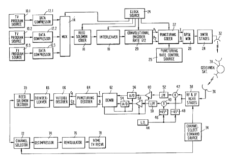
Reference is now made to Fig. 1, a block diagram of
a complete system including certain features of the
present invention, wherein television program sources
10.1, 10.2 and 10.3 respectively supply baseband audio
and video signals to data compressors 12.1, 12.2 and
12.3. Compressors 12.1, 12.2 and 12.3 derive sequential
binary bit wavetrains respectively indicative of
frequency compressed versions of audio and video
W094/286~6 PCT~S94/05837
~11408~1
information of sources 10.1, 10.2, 10.3. The binary
wavetrains derived from compressors 12.1, 12.2 and 12.3
are combined in time division multiplexer 14 to form a
single binary signal that is supplied to Reed-Solomon
encoder 16. The resulting serial binary bit wavetrain
derived from Reed-Solomon encoder 16 is supplied to
conventional interleaver 18, having an output feed to
one-half rate convolutional encoder 20. Convolutional
encoder 20 derives a pair of parallel binary bit streams
Pl and P2 having sequential bits Pl(0), Pl(l), Pl(2) etc.
and P2(0), P2(1), P2(2) in time slots 0,1,2 etc. The Pl
and P2 outputs of encoder 20 are punctured by puncturing
encoder 22. Each of multiplexers 14, coder 16,
interleaver 18 and coder 22 is responsive to pulses from
clock source 24. Puncturing encoder 22 responds to
signals from encoder 22 and clock source 24, as well as
a punctured code command signal from operator controlled
source 25, to derive a pair of parallel punctured serial
binary bit streams which are applied to I and Q inputs of
quadrature phase shift key modulator 26.
Modulator 26 responds to the binary bit streams
supplied to it to derive a quadrature phase shift key
wavetrain, supplied to transmitter 28, having an output
radiated by antenna 32 to a transponder or repeater on
geosynchronous satellite 30. Circuitry on geosynchronous
satellite 30 responds to the signal from transmitter 28
and antenna 32 to emit a microwave signal having an
extremely wide beam width to numerous terrestrial
receiving sites, one of which is illustrated in Fig. 1.
The signal transmitted from satellite 30 to the
terrestrial receiving site is typically in either C or Ku
band.
A typical terrestrial receiving site includes
reflecting antenna dish 36 having a diameter no greater
than approximately one meter and optimally having a
parabolic shape; in first and second specific
embodiments, antenna dish 36 respectively has diameters
of 60 and 90 centimeters. The signal transduced by an
active element coupled with dish 36 is amplified and down
- 12 - 2 ~ 4~5 ~
converted to an IF frequency by RF and IF stages 38
responsive to an operator controlled channel select
signal from source 39. Stages 38 have an IF analog
output applied in parallel to mixers 40 and 42, driven by
the output of fixed frequency local oscillator 44 via
+45~ phase shifters 46 and 48. The outputs of mixers are
supplied to matched lowpass filters 50 and 52, having I
and Q baseband outputs that are respectively applied to
analog to digital converters 54 and 56 via variable gain
amplifiers 58 and 60 for normalizing the amplitude of the
input signals to the converters so the maximum analog
input level applied to the converters equals the maximum
voltage level the converters are designed to handle.
Converters 54 and 56 respond to the I and Q baseband
signals supplied to them to derive multi-bit digital
signals having values commensurate with the magnitude and
polarity of the I and Q baseband signals supplied to the
converters so the most significant bits derived from the
converters represent polarity while the remaining bits
represent amplitude.
Analog to digital converters 54 and 56 respond to
the analog outputs of amplifiers 58 and 60 -and to
sampling pulses to derive multi-bit digital signals which
are supplied to demodulator 62, preferably configured as
disclosed in the co-pending, commonly assigned Canadian
application Serial No. 2,130,269 of Itzhak Gurantz, Yoav
Goldenberg and Sree Raghavan, entitled "Demodulator for
Consumer Uses," filed December 29, 1993. Demodulator 62
derives (1) sampling pulses which are supplied to analog
to digital converters 54 and 56, (2) gain control signals
for variable gain amplifiers 58 and 60, (3) a carrier
tracking error signal used in the demodulator to correct
for frequency and phase errors of local oscillator 44
relative to the frequency and phase of the IF output of
stages 38, and (4) I and Q channel output signals. For
each sample taken by converters 54 and 56 demodulator 62
derives three parallel binary output bits in each of the
I and Q output channels thereof. The most significant
bit of each triad of bits represents the
W094/~656 21 ~ 0 8 51 PCT~S94/05837
13
polarity of the sample, as corrected by the carrier
tracking circuit, and the two additional binary bits
provide a measure of the quality of the first bit, as
corrected by the carrier tracking circuit. The most
significant bit of each three bit triad in the output of
demodulator 62 thus indicates the binary value associated
with each sample taken by converters 54 and 56 and the
two least significant bits indicate a confidence factor
for the binary value of the most significant bit.
The I and Q channel output signals of demodulator 62
are supplied to puncturing decoder 64, set for the
punctured code of puncturing coder 22 at the transmitter,
i.e., either 2/3 or 6/7. Decoder 64 is set by an
operator for the correct punctured code or the rate can
be automatically controlled. Puncturing decoder 64
responds to the I and Q outputs of demodulator 62 to
derive binary indication of each sample taken by
converters 54 and 56; the binary outputs of decoder 64
associated with the I and Q channels derived by
demodulator 62 are data sequences respectively indicated
as G1 and G2. Decoder 64 also derives on leads 65 and 67
signals indicating whether or not the simultaneously
derived Gl and G2 outputs thereof are dummy bits.
Puncturing decoder 64 also inserts dummy bits in time
slots corresponding to the time slots which were
punctured, i.e., deleted, by puncturing coder 22 at thè
transmitter and derives a punctured data clock having a
rate corresponding and synchronized with the G1 and G2
data sequences.
All of the aforementioned outputs of puncturing
decoder 64 are supplied to Viterbi decoder 66 which
derives a single serial binary signal train that is quite
similar to the binary wavetrain applied to encoder 20.
The binary serial signal train derived by Viterbi decoder
66 is supplied to de-interlever 68, having an output
supplied to Reed-Solomon decoder 70, having a multi-bit
serial output that is an approximate replica of the
signal supplied to Reed-Solomon coder 16 at the
transmitter.
W094/28656 PCT~S94/05837
~4~a5~ 14 '~~
The binary output signal of Reed-Solomon decoder 70
is applied to channel selector 72, responsive to the
channel select signal from a television receiver at the
receiver site. Channel selector 72 selects the binary
bits in the output of Reed-Solomon decoder 70 associated
with the television program source lO.1, 10.2 or 10.3
selected by a user of the television receiver at the
receiving site. The binary bits associated with the
selected program source are coupled to video decompressor
74 to the exclusion of the binary bits associated with
the other program sources at the transmitter site. Video
decompressor 74 responds to the binary signal values
supplied to it to derive an analog signal that is an
approximate replica of the audio and video information of
the selected one of program sources 10.1-10.3.
The analog output signal of decompressor 74 is
supplied to remodulator 76 which converts the signal
supplied to it to a conventional television signal in any
of the usual formats, such as NTSC, PAL, or SECAM. The
signal derived from remodulator 76 is modulated on a
standard broadcast television carrier frequency, such as
the carrier frequency associated with channel 3 or 4, as
selected by a switch at the receiver site. The standard
television signal thereby derived by remodulator 76 is
supplied to conventional home television receiver 78.
Alternatively, elements similar to elements 38-76 are
incorporated in a home television receiver.
The system of Fig. 1 has been previously proposed by
others, except that the previously proposed punctured
codes for puncturing coder 22 and puncturing decoder 64
were 2/3 and 7/8. It has been previously established
that the 2/3 punctured code is to be emitted from the
circuitry on satellite 30 at the 10-watt level and that
the other punctured code is to be emitted from the
satellite at 20 watts. By performing a bit error ratio
analysis, we found the 7/8 punctured code is excessive
for successful operation of the system with 20-watt
emissions from geosynchronous satellite 30, but that 20-
watt emissions at a 6/7 punctured code is acceptable.
W094/286~6 2 ~ 4 0851 PCT~S94/05837
When coder 22 is set for puncturing at the 2/3 rate,
1 1( )r 1(2), Pl(3), Pl(4) in bit stream P
in time slots tor t1, t2, t3, t4 and bits P2(0), P2(1),
P2(2), P2(3), P2(4) in bit stream P2 in the corresponding
time slots, are converted by puncturing coder 23 into I
and Q signals that are supplied to modulator 26 in
accordance with:
Table IV
tk tk+l tk+2 tk~3
I Pl(0)P2(l)P2(2)Pl(4)
10 Q P2(0)P~(2)P2(3)P2(4)
k~ tk+1, tk+2, tk+3 are sequential time slots
for the output of coder 22.
Coder 22 responds to subsequent bits in bit streams
P1 and P2 in a manner similar to that described for bits
P1(0) Pl(4) and bits P2(0) P2(4) to derive subsequent I
and Q outputs of the coder. To these ends, coder 22
includes a puncturing code for bits P1(0), Pl(1), P2(0),
P2(1) in accordance with
Table V
to tl
ERI 1 0
ER2
where ER1 is the puncturing code for bits Pl(0),
pl(l),.. -Pl(ti)r Pl(tj+l)
ER2 is the puncturing code for bits P2(0),
p2(1)...P2(tj)~ P2(tj+1)
tj is an even numbered time slot
1 indicates the bit is not punctured
0 indicates the bit is punctured.
The puncturing code of Table V is applied to bit streams
P1 and P2 as follows:
W094/286~6 PCT~S94/05837
2 ~4~S ~ 16
Table VI
Pl Pl(O) Pl(l) Pl(2) Pl(3) Pl(4)
P2 P2(0) P2(l) P2(2) P2(3) P2(4)
where X indicates the bit is punctured.
In one preferred embodiment of the invention, the
unpunctured bits of Table VI are formed into a serial
signal in accordance with:
P (0),P2(0),P2(1),P1(2),P2(2),P2(3),P1(4),P2( ) ( )
Odd numbered bits in Expression (1), i.e., bits Pl(0),
P2(1), P2(2), P1(4), are coupled by coder 22 to the coder
I output, while even numbered bits in Expression (1),
2 )~ P2(3), P2(4), are coupled to the
coder Q output thereby to form the I and Q bit sequences
of Table IV.
When puncturing coder 22 is set to puncture at the
6/7 rate, sequential bits in time slots to ~ tll of the
Pl and P2 outputs of encoder 20 are converted by coder 22
into I and Q channel output signals in accordance with
Table VII
tk t~+l tk+2 tk+3 tk+4 t~+5 tk+6
I Pl(0) P2(1) Pl(3) Pl(5) P2(6) P2(8) P2(10)
Q P2(0) P2(2) P2(4) Pl(6) P2(7) Pl(9) Pl(11)
Coder 22 responds to subsequent bits in bit streams Pl
and P2 in a manner similar to that described for bits
P1(0) Pl(11) and P2(0) P2(11) to derive subsequent I and
Q output bits of the coder. To these ends, coder 22
includes a puncturing code for bits Pl(0) Pl(5) and P2(0)
P2(5) in accordance with:
W094/28656 214 0 8 51 PCT~S94/05837
17
Table VIII
t; tj+~ t ~+2 t i+3 t i+4 t i+5
ERI 1 0 0 1 0
ER2 1 1 1 0 1 0
In one embodiment, the puncturing code of Table VIII is
applied to bit streams Pl and P2 as follows:
PCT/US94/05837
WO 94/28656
?.~4~
18
_
-- ':
.
P~
X _ _
_1 ~
~ _ _
~ P~
.
P~
~ P~
o o
~ P~
-
W094l28656 2 ~ ~ 0 8 S 1 PCT~S94/05837
."~
19
The unpunctured bits of Table IX are formed into a serial
signal in accordance with:
Pl(O)I P2(0), P2(1), P2(2), Pl(3), P2(4), Pl(5),
2 ) 2( )I P2(8), P1(9), P2(1~)~ P1(11) (2)
Odd numbered bits in Expression (2), i.e., bits P1(0),
1 1 ) 2( )I P2(8), P2(10), are coupled to
the I output of coder 22, while even numbered bits in
Expression (2), i.e., bits P2(0), P2(2), P2(4), P1(6),
P2(7), Pl(9), Pl(ll), are coupled to the Q output of the
coder, thereby to form the bit sequences of Table VII.
Similarly, but in an opposite manner, decoder 64 is
set to punctured code 2/3 or 6/7. Decoder 64 responds to
the I and Q output signals of demodulator 62 and
separates these signals into signals Gl and G2, similar
to the Pl and P2 inputs of puncturing coder 22, and
designates which bits derived from the decoder are
associated with bits which have been punctured by coder
22. Decoder 64 includes puncturing codes identical to
the puncturing codes of Tables V and VIII for the 2/3 and
6/7 rates.
When puncturing decoder 64 is set at the 2/3
punctured code, it responds to sequential bits of the I
and Q bit streams derived by demodulator 62 and the code
of Table V to derive Gl and G2 output signals that are a
close replica of the Pl and P2 signals supplied to
puncturing coder 22 such that sequential bits I(0) I(8)
and Q(0) Q(8) of channels I and Q in time slots to-t
are derived in accordance with:
WO 94/28656 PCT/US94/05837
2~4o35l
~ 20
X
_I
~ ~ ~.
-
X
~ a
X
X _ _
a ~
~a
E~ _
X
H 0
O O
0
C~
W094/28656 2 1 4 0 8 S1 PC~S94/05837
where X designates a "dummy bit," i.e., a bit having a
value that is not related to the value of a bit in I(0)
I(8) or Q(0) Q(8). To form the bit sequences of Table X
in one embodiment, bit sequences I(0) I(8) and Q(0) Q(8)
and the deletion pattern of Table V are combined to form
a serial sequence including dummy bits X as follows:
I , Q(0)~ X~ Q(l)r I(2)~ ' (2)
I(3), Q(3), X, I(4), Q(4), I(5), , (5)
(6)' Q(6)~ X~ I(7)~ Q(7), I(8), X, Q (3)
Decoder 64 couples the bit sequence of Expression (3) to
the Gl and G2 outputs thereof so the odd and even
numbered bits of the sequence are respectively derived at
the Gl and G2 outputs in accordance with Table X.
When puncturing decoder 64 is set at the 6/7 rate, it
responds to the sequential bits in the I and Q bit
streams at the output of demodulator 62 and the
puncturing code of Table VIII to derive Gl and G2 bit
sequences in accordance with:
WO 94/28656 PCT/US94/05837
2~408s~
22
~o .
a
_
~O .
H
In
a x
X X
~ _ _
a H
X
~ X
-
a
~ _I
H
H a
~ ~7
W094/28656 21 4 0 8 5 1 PCT~S94/05837
~, _
23
To form the bit sequences of Table XI in one embodiment,
bit sequences I(0) I(6) and Q(0) Q(6) and the deletion
pattern of Table VIII are combined to form a serial
sequence including dummy bits X as follows:
I(0), Q(0), X, I(l), X, Q(1), I(2), X, X,
Q(2), I(3), X, Q(3), I(4), X, Q(4), X,
I(5), Q(5), X, X, I(6), Q(6), X (4)-
Decoder 64 couples the bit sequence of Expression (4) to
the G1 and G2 outputs thereof so the odd and even
numbered bits of the sequence are respectively derived at
the Gl and G2 outputs in accordance with Table XI.
Inspections of Tables X and XI indicate there are
repetitive dummy bit patterns in these Tables; in Table
X the dummy bit pattern repeats after every other pair of
time slots; in Table XI the bit pattern of the first six
time slots repeats in the second set of time slots. The
serial stream of Expression (3) is formed by serializing
bit streams I and Q so I(k) is immediately before Q(k)
and Q(k) is immediately before I(k+l); then a dummy bit
is inserted at the third time slot in each sequence of
- four bits in the final serialized bit stream; e.g. the
first dummy bit follows bits I(0), Q(0) and is
immediately before I(l) to form the first four bits in
the final serialized bit stream. The serial stream of
Expression (4) is formed by serializing bit streams I and
Q and inserting dummy bits at the third, fifth, eighth,
ninth and twelfth time slots in each sequence of 12 bits
in the final serialized bit stream. Insertion of the
dummy bits into the final serialized bit streams is
controlled by the positions of the "0' values in Tables
V and VIII.
Reference is now made to Fig. 2, a block diagram of
a universal apparatus for converting data bit streams P1
and P2 on leads 200 and 202, as derived from
convolutional encoder 20, into a pair of punctured I and
Q channel bit streams. The apparatus of Fig. 2 can be
used on bit streams P1 and P2 for any of the optimum
punctured codes disclosed by Yasuda et al., i.e. 1/2,
2/3, 3/4, 4/5, 5/6, 6/7, 7/8, 8/9, 9/10, 10/11, 11/12,
W094/28656 PCT~S94/05837
2~ 40~5 ~ 24
12/13, 13/14, 14/15, 15/16, 16/17. The data bits on
leads 200 and 202 are supplied to electronic multiplexer
204, operated at a frequency twice the rate of data on
leads 200 and 202 in response to a square wave data clock
at terminal 206. The data clock at terminal 206 and the
data on leads 200 and 202 have the same frequency and
phase, a result achieved by conventional synchronizing
circuitry (not shown). Multiplexer 204 responds to one
levels at terminal 206 to switch the signal on lead 200
to output lead 208; in response to a zero level at
terminal 206, the signal on lead 202 is coupled to output
lead 208.
The resulting serial bit sequence Pl(0), P2(0),
Pl(l), P2(1), Pl(2), P2(2) etc. on lead 208 is supplied
to data input terminal 210 of first in first out register
(FIFO) 212, including clock input terminal 214. Clock
input terminal 214 responds to a punctured data clock
derived from AND gate 216, having one input responsive to
a pulse train from clock source 218, which derives clock
pulses that are synchronized with and have a frequency
twice the frequency of clock pulses at terminal 206. The
clock pulses derived from source 218 are coupled directly
to one input of AND gate 216, while input terminal 206 of
multiplexer 204 responds to the pulses from clock source
218, as modified by divide by two frequency divider 220.
The other input of AND gate 216 is derived by
supplying the data clock output of frequency divider 220
to a count input of counter 222, having a multibit output
applied to address input 224 of memory 226. Counter 222
and memory 226 respond to a control signal from source
227 indicative of which of the deletion codes specified
in the Yasuda et al. article is to be used. Counter 222
is set to a maximum count in response to the control
signal from source 227 and is continuously sequenced from
zero to its maximum count by the data clock pulses from
divider 220. The count in generator 222 controls the
address input of memory 224.
Memory 226 is loaded with a pair of deletion
patterns for each of the deletion codes specified in the
W094/28656 PCT~S94/0~837
~ 2140851
Yasuda et al. article. Selection of a deletion code is
by control source 227. Sequential bits of the two
deletion patterns of the selected deletion code are
supplied to leads 228 and 230 by memory 226 in response
to the sequential addresses supplied to input 224. For
example, if the selected deletion code is rate 2/3,
generator 222 responds to the first three data clock
pulses from divider 220 to supply addresses 0000, 0001,
0000 in sequence to address input 224 and memory 226
responds to these address signals to supply leads 228 and
230 with the sequential binary bits 10 and ll,
respectively; the sequences on leads 228 and 230
respectively correspond with the sequences on lines 1 and
2 of Table V. A similar sequence is derived on leads 228
and 230 in response to each succeeding triad of
sequential data clock pulses. If control source 227 is
set for the 6/7 punctured code, address generator 222
responds to the first six data clock pulses from divider
220 to derive the addresses 0000, 0001, 0010, 0011, 0100,
0101 which cause memory 226 to supply leads 228 and 230
with the binary sequences 100101 and 111010,
respectively; these sequences correspond with the
sequences on lines 1 and 2 of Table VIII and are repeated
for every six sequential data clock pulses.
For the aforementioned 2/3 situation the bit
sequences on lead 234 and at the output of AND gate 216
are respectively repeating sequences of 1101 and
10100010; for the 6/7 situation the bit sequences on lead
234 and at the output of AND gate 216 are respectively
repeating sequences of 110101100110 and
101000100010100000101000. FIFO 212 responds to the
leading edge of each 1 in the output of AND gate 216 to
clock the binary value which is simultaneously at
terminal 210 into the FIFO. Binary values which occur at
terminal 210 while the output AND gate 216 is 0 are not
coupled into FIFO 212, hence are deleted, i.e.
punctured. For the 2/3 situation, FIFO 212 responds to
the serial combination of the P1 and P2 signals at
terminal 210 and the punctured clock at terminal 208 to
W094/286~6 PCT~S94/05837
21 408S~ 26
be loaded with the punctured sequence P1(0), P2(0),
2 1 2( )' 2(3)' Pl(4), P2(4) etc. For the
6/7 situation, FIFO 212 is loaded with the punctured
sequence Pl(0), P2(0)~ P2(1)' P2(2)' 1( ) 2
1( )' P2(6)~ P2(7)~ P2(8) etc.
FIFO 212 includes data output terminal 236 and clock
terminal 238 for controlling the rate at which bits are
supplied by the FIFO to terminal 236. Terminal 238
responds to symbol clock source 240, having a frequency
equal to two times the frequency symbols are supplied to
I and Q outputs 243 and 244. The clock pulses derived
from clock source 240 are supplied via divide by two
frequency divider 239 to serial to parallel converter,
i.e. demultiplexer, 242, having a data input responsive
to pulses at output 236 of FIFO 212. Converter 242
responds to the clock pulses from source 240 such that
the signal at terminal 236 is coupled to leads 243 and
244 while the clock pulses have zero and one values,
respectively. Because of puncturing, the symbol rate is
less than the data rate ; in one embodiment the data rate
on leads 200 and 202 is 20 megabits per second while the
symbol rate on leads 243 and 244 is 15 megabits per
second for the 2/3 punctured code.
FIFO 212 responds to the sequence loaded into it and
the clock at terminal 238 to derive at terminal 236 the
same serial sequence as is loaded into the FIFO at
terminal 210. The sequence is read from terminal 236 at
the clock frequency applied to terminal 238, which is
twice the symbol clock. For the 2/3 rate, demultiplexer
242, which switches at twice the symbol clock rate in
response to the opposite levels of the symbol clock
frequency output of divider 239, responds to the sequence
at terminal 236 so the I(0), I(l), I(2), I(3), I(4) and
Q(0), Q(l), Q(2), Q(3), Q(4) sequences on leads 243 and
244 are respectively Pl(0), P2(1), P2( )~ 1( )
P2(0), Pl(2), P2(3), P2(4) etc.; for the 6/7 rate the
sequences on leads 243 and 244 are respectively P1(0),
2 1 ) 1( )' P2(6)' P2(8), P2(10) etc. and
P (0) P (2), P2(4), P1(6), P2(7), Pl(9), 1(
W094/28656 ~14 0 8 51 PCT~S94/05837
.~_
27
Reference is now made to Fig. 3 of the drawing, a
block diagram of a preferred embodiment of puncturing
decoder 64. The puncturing decoder illustrated in Fig.
3 has an architecture very similar to the architecture of
the puncturing coder illustrated in Fig. 2, enabling the
puncturing coder and puncturing decoder to be fabricated
from the same printed circuit mask, with very slight
changes in connections. The puncturing decoder
illustrated in Fig. 3 is also universally applicable to
all of the optimum punctured codes disclosed by Yasuda et
al.
The puncturing decoder illustrated in Fig. 3
includes multiplexer 304, FIFO 312, demultiplexer 342,
AND gate 316, counter 322, memory 326 and multiplexer
332, which correspond with corresponding elements 204,
212, 242, 216, 222, 226 and 232 of Fig. 2. Multiplexer
304 responds to the I and Q outputs of demodulator 62,
and has an output connected to a data input of FIFO 312
in the same manner as the output of multiplexer 204 is
coupled to the data input of FIFO 212. The data output
of FIFO 312 is supplied to an input of demultiplexer 242
in the same manner that the data output of FIFO 212 is
connected to the input of demultiplexer 342.
Demultiplexer 342 derives G1 and G2 bit sequences
including dummy bits that are supplied to Viterbi decoder
66. Counter 322, memory 326, multiplexer 332 and AND
gate 316 are connected to each other in the same manner
that counter 222, memory 226, multiplexer 332 and AND
gate 216 are connected to each other.
The puncturing decoder of Fig. 3 also includes
square wave clock sources 318 and 340, respectively
having frequencies equal to twice the frequency of data
sequences Gl and G2 supplied by demultiplexer 342 to
leads 343 and 344 and twice the frequency of the I and Q
symbols supplied to multiplexer 304 via leads 300 and
302. Clock sources 318 and 340 are synchronized to the
received symbols in a manner well known to those skilled
in the art, by apparatus not shown. The output of symbol
clock 318, at two times the rate of data sequences Gl and
W094/28656 PCT~S94/05837
2140851 28 1~
G2 is applied to AND gate 316 so that AND gate 316
derives a punctured clock sequence in identically the
same manner that AND gate 216 derives a punctured clock
sequence. The output of AND gate 316 is supplied to
terminal output data clock 338 of FIFO 312; in contrast,
the terminal output data clock of FIFO 212 responds to a
frequency equal to twice the symbol frequency, as derived
from clock source 240. FIFO 312 responds to positive
going leading edges at terminal 338 so that the FIFO
derives, at terminal 336, a binary bit sequence that is
the same as the bit sequence supplied to the FIFO.
Demultiplexer 342 includes a control input having a
frequency equal to the frequency of data in sequences Gl
and G2, as derived from divide by 2 frequency divider
320, in turn responsive to the output of data clock
source 318. Thereby, lead 343 is responsive to the
binary level at terminal 336 when the output of frequency
divider 320 has a binary 1 value and the output at
terminal 336 is supplied to lead 344 while the divider
output has a binary 0 level. Hence, demultiplexer 342 is
switched at twice the frequency of data clock source 318.
The output of clock source 340, at twice the
frequency of the I and Q symbols on leads 300 and 302, is
supplied to the data clock input terminal 314 of FIFO
312. Control input 306 of multiplexer 304 responds to a
divide by two output of clock source 340, as derived from
divide by two frequency divider 339, so the I and Q bits
on leads 300 and 302 are alternately coupled to data
input 310 of FIFO 312 via lead 308 at twice the frequency
of the I and Q symbols on leads 300 and 302. Counter 322
and memory 326 respond to signals from control source 327
indicative of which of the optimum codes is being
transmitted to the receiver. Control source 327 can be
controlled by a signal derived from the transmitter at
the time a transmission sequence begins or in other ways.
For the 2/3 punctured code, the sequential I and Q
symbols supplied to leads 300 and 302 are respectively
represented as:
WO 94/28656 214 0 8 5 1 PCT/US94/05837
29
I(0), I(l), I(2), I(3), I(4), I(5), etc. (5) and
Q(0), Q(l), Q(2), Q(3), Q(4), Q(5), etc. (6)
Multiplexer 304 responds to the I and Q sequences on
leads 300 and 302 to derive on lead 308 a signal in
accordance with:
I(0) ~ Q(0) ~ I(l), Q(l), I(2), Q(2), I(3), Q(3),
I(4)~ Q(4), I(5)~ Q(5), etc. (7).
The foregoing sequence of binary bits is loaded into FIFO
312, which responds to the punctured clock derived from
AND gate 316 to derive, on lead 336, the sequence:
I(0)~ Q(0)~ X~ I(l)~ Q(l), I(2)~ X, Q(2)~ I(3)~
Q(3), X, I(4), Q(4), I(5), X, Q(5), etc., (8).
where X is a "dummy" bit at output 336.
Demultiplexer 342 responds to the foregoing sequence at
terminal 336 to supply leads 343 and 344 with sequences
Gl and G2, respectively, in accordance with:
Gl = I(0), X, Q(l), X, I(3), X, Q(4), X, etc. (9) and
G2 = Q(0), I(l), I(2), Q(2), Q(3), I(4),
I(5), Q(5), etc. (10).
Substitution of the Pl and P2 values supplied to
puncturing coder 22 for the values of:
I(0), I(l), I(2)~ I(3), I(4), I(5), etc. and
Q(0), Q(l), Q(2), Q(3), Q(4), Q(5), etc.
indicates the output of puncturing decoder 64 is ordered
in the same manner as the input to puncturing coder 22,
except for the insertion of the dummy bits. The presence
of the dummy bits is signalled to Viterbi decoder 66 by
the output of multiplexer 332 by a O at the output of the
multiplexer.
For the 6/7 punctured code, the inputs and output of
multiplexer 304 and the data input 310 of FIFO 312 are
identical to the previously described situation for the
2/3 punctured code. However, for the 6/7 situation, the
output of AND gates 216 and 316 differs from that for the
2/3 rate; the output of AND gates 216 and 316 for the 6/7
punctured code are identical. FIFO 312 responds to the
punctured data clock output of AND gate 316 and the
signal supplied to it to derive, at terminal 336, a
sequence in accordance with:
W094/28656 PCT~S94/05837
40a~ ~ 30
I(0), Q(0), X, I(l), X, Q(1),
I(2), X, X, Q(2), I(3), X (11).
Demultiplexer 342 responds to the sequence at output 336
of FIFO 312 to derive, on leads 343 and 344, data
sequences in accordance with:
I(0), X, X, I(2), X, I(3), etc. (12) and
Q(0), I(1), Q(l), X, Q(2), X, etc. (13).
The apparatus illustrated in Fig. 3 is for a
situation in which demodulator 62 derives a single bit
for each I and Q symbol. However, in many situations,
demodulator 62 derives a most significant bit indicative
of the values of I and Q and one or more additional bits
indicative of the confidence levels of the most
significant bits for the proper values of I and Q. The
additional bits are derived in parallel with the most
significant I and Q bits and have corresponding time
slots. The additional bits are processed by apparatus
similar to that illustrated in Fig. 3, such that for each
additional bit a multiplexer, FIFO and demultiplexer are
provided. The multiplexer, FIFO and demultiplexer for
the additional bits are driven in parallel by the same
data clock pulse trains, punctured data clock pulse
trains and symbol clock pulse trains which drive
multiplexer 304, FIFO 312 and demultiplexer 342. The
additional bits are applied to Viterbi decoder 66 and
processed by the Viterbi decoder, interleaver 68 and
Reed-Solomon decoder 70 in a manner well known to those
of ordinary skill in the art.
Reference is now made to Fig. 4 of the drawing, a
block diagram of a second embodiment of puncturing coder
22, specifically designed only for deriving the 2i3 and
6/7 punctured signals in response to the Pl and P2 output
signals of rate 1/2 encoder 20. Signals Pl and P2
derived by encoder 20 are respectively applied to D
inputs of D (data) flip-flops 422 and 424, having clock
(CK) inputs responsive to square wave data clock source
400, also coupled to encoder 20 to control the rate, i.e.
frequency, at which the Pl and P2 signals are read from
the encoder. Signals at the Q output terminals of flip-
W094/~.656 2 1 ~ ~ 8 5 1 PCT~S94/0~837
31
flops 422 and 424 are respectively applied to "0" signal
input terminals of two input signal multiplexer 418 and
three input signal multiplexer 420. Multiplexer 418
includes a "1" input signal terminal responsive to the
signal at the Q output of flip-flop 424, while
multiplexer 420 includes a "1" input signal terminal
responsive to the Pl output of encoder 20. The P2 output
of encoder 20 is coupled to input signal terminal "2" of
multiplexer 420. Multiplexer 418 includes a single bi-
level (0 and 1) control input terminal, while multiplexer
420 includes two bi-level control input terminals.
Multiplexers 418 and 420 are activated so an output
signal is always simultaneously derived from them. The
output signals of multiplexers 418 and 420 are applied to
parallel signal input terminals of FIFO 430, from which
are derived I and Q symbol representing signals. Output
signals of FIFO 430 are derived at a rate equal to one-
half the frequency of symbol clock source 436 which
drives the FIFO output clock terminal via divide by two
frequency divider 438. The rate at which bits are
coupled to the signal input terminals of FIFO 430 is
controlled by AND gate 432, in turn responsive to a
logical combination of the output of data clock 400 and
a puncture control signal derived from multiplexer 434.
The output of gate 432 is applied to the FIFO input clock
terminal. The I and Q symbol representing signals
derived by FIFO 430 are respectively responsive only to
the outputs of multiplexers 418 and 420.
Control of multiplexers 418 and 420 is provided by
logic network 406, including multiplexers 412, 416 and
434. AND gate 432 responds to the signal supplied to it
by multiplexer 434 and the square wave output of clock
400 to derive a punctured output clock having a
predetermined "frequency". The punctured output of gate
432 is a sequence of binary 1 and 0 levels, arranged so
certain binary 1 levels are deleted from the square wave
output of clock source 400. For rate 2/3, gate 432
responds to the signals supplied to it by multiplexer 434
and a 10101010 sequence from clock source 400 to derive
W094/28656 PCT~S94/OS837
'1.~ 40~5~ 32
the sequence lO101000. For rate 6/7, gate 432 responds
to the signal supplied to it by multiplexer 434 and a
lO1010101010101010101010 sequence from clock source 400
to derive the sequence 101000100010100010001000. Each of
the aforementioned sequences derived from gate 432 is
thereafter repeated. Hence, for the output of gate 432
having a "frequency~' of CKout~ the square wave derived
from clock source 400 has a frequency CKin = 1.333CKoU~ for
a 2/3 puncturing rate; for the 6/7 puncturing rate, the
frequency, CK1n, of the square wave derived from clock
400 is 1.71429 CKout~ To these ends, multiplexer 416
includes two output leads on which are derived four
possible binary bit values for control of multiplexer
420; only three of the four values are used. Multiplexer
412 includes a single output lead on which are derived
two binary bit levels for controlling the state of
multiplexer 418. The output combinations of multiplexer
416 control whether the signal at 0, 1 or 2 signal input
terminal of multiplexer 420 is passed to the output of
that multiplexer or if the output of the multiplexer 420
is decoupled from the signals at its signal input
terminals.
Control of multiplexers 412, 416 and 434 is in
response to the binary level derived from rate control
source 408. Rate control source 408 derives binary O and
1 levels when the 2/3 and 6/7 puncture rates are
respectively selected. The binary output of source 408
is applied in parallel to control input terminals of
multiplexers 412, 416 and 434. In response to the binary
0 and 1 levels of source 408, the inputs at the "O~ and
~ signal input terminals of multiplexers 412, 416 and
434 are respectively coupled to the signal output
terminal of each multiplexer.
Signals applied to the O and 1 signal input
terminals of multiplexers 412, 416 and 434 are derived by
applying the output of data clock 400 to 12 state counter
402, having a count ranging from O to 11 and a four bit
output bus. The two least significant output bits of
counter 402 are supplied to logic network 440, which
W094l~656 21 4 0 8 51 PCT~S94/05837
33
derives a binary 1 level in response to these bits having
a value indicative of the numerics 0, 1 or 2, (binary
values 00, 01, 10), and a binary 0 level in response to
the two least significant bits having a numeric value of
3 (binary value 11). The output of logic network 440 is
applied to the 0 signal input terminal of multiplexer
434. All four binary output bits of counter 402 are
supplied to logic network 442, which derives a binary 1
value in response to the counter output representing any
of the numerics 0, 1, 3, 5, 6, 8 or 10; logic circuit 442
derives a binary 0 value in response to the four bits
derived from counter 402 representing any of the numerics
2, 4, 7, 9 or 11~ The binary level derived from logic
network 442 is applied to the "1" input signal terminal
of multiplexer 434. The resulting output of multiplexer
434 is applied to AND gate 432 to control the coupling of
data bits from multiplexers 418 and 420 into FIFO 430.
The 0 and 1 signal input terminals of multiplexer
412 respectively respond to outputs of logic networks 444
and 446, both in turn responsive to the four-bit output
of counter 402. Network 444 derives a binary 1 output in
response to the output bits of counter 402 representing
any of the numerics 1-3, 5-7 or 9-11; logic network 444
derives a binary 0 output in response to the four-bit
output of counter 402 representing any of the numerics 0,
4 and 8. Logic network 446 responds to the four-bit
output of counter 402 to derive a binary 1 level in
response to the output of the counter representing any of
the numerics 1, 2, 4 or 6-11. A binary 0 level is
derived from logic network 446 in response to the count
of counter 402 representing any of the numbers 0, 3 or 5.
Multiplexer 416 includes one control input terminal,
first and second output terminals and four signal input
terminals, designated as first and second "0" signal
input terminals and first and second "1" signal input
terminals. In response to a binary zero being applied to
the control input terminal the binary levels at the first
and second "0" signal input terminals are respectively
coupled to the multiplexer first and second output
W094/286~6 PCT~S94/05837
~2~ S~ 3
~ terminals; in response to a binary one being at the
control input terminals the levels at the first and
second "1" signal terminals are respectively coupled to
the multiplexer first and second output terminals.
The most and next most least significant output bits
of counter 402, representing the numerics 0-3, are
respectively applied to the first and second 0 signal
input terminals of multiplexer 416 and coupled to the
multiplexer first and second output terminals, thence to
the control inputs of multiplexer 420, in response to a
binary 0 output of source 408 being applied to the
control input of multiplexer 416. The first and second
1 input signal terminals of multiplexer 416 are
respectively responsive to first and second output bits
of logic network 448, in turn responsive to all four
output bits of counter 402. In response to the count of
counter 402 representing the numeric 0, logic network 448
supplies a binary 0 level to each of the first and second
1 signal input terminals of multiplexer 416. In response
to counter 402 deriving a signal representing the
numerics 5, 8 and 10, a binary 1 signal is applied by
network 448 to the first "1" signal input terminal of
multiplexer 416, while a 0 level is applied to the second
"1" signal input terminal of the multiplexer. For all
other numeric values for the outputs of counter 402, a
binary 0 level is supplied by logic network 448 to the
first "1" input terminal of multiplexer 416 while a
binary 1 level is supplied to the second 1 input terminal
of multiplexer 416. Hence, in response to control source
408 deriving a binary 1 level while counter 402 is
deriving the binary sequence 0000, multiplexer 416
supplies signal bits 00 to the control input of
multiplexer 420 to couple the signal at the Q output of
flip-flop 424 to the output of multiplexer 420. While
source 408 derives a binary 1 level and counter 402
derives a binary signal associated with the numerics 5,
8 and 10, multiplexer 416 supplies signal levels 1 and 0
to the control inputs of multiplexer 420, causing the P1
output of encoder 20 to be coupled to the output of
W094/~656 21 ~ 0 8 51 PCT~S94/05837
multiplexer 420. In response to source 408 deriving a
binary 1 level while counter 402 derives a binary signal
associated with the numerics 1, 2, 3, 4, 6, 7, 9 and 11,
multiplexer 416 supplies multiplexer 420 with signal bits
0 and 1, causing multiplexer 420 to supply the P2 output
of encoder 20 to the signal input terminal of FIFO 430.
The I and Q channel signals derived from FIFO 430
have sequences identical to the sequences derived from
demultiplexer 242 for the 2/3 and 6/7 puncturing rates.
The circuitry of Fig. 4 processes the Pl and P2 sequences
derived from encoder 20 on a parallel basis. The
parallel sequences are punctured by FIFO 432 that derives
the parallel I and Q channels. The circuitry of Fig. 4
does not include a ROM and its associated control
circuitry as is required by the circuitry illustrated in
Fig. 2. However, the circuitry of Fig. 4 does not have
the advantage of being universally applicable to all of
the optimum puncturing rates disclosed by Yasuda et al.
Reference is now made to Fig. 5 of the drawing,
a block diagram of a second embodiment of puncturing
decoder 64, particularly applicable to the 2/3 and 6/7
punctured codes. The apparatus illustrated in Fig. 5 is
responsive to the I and Q outputs of demodulator 62 and
includes square wave symbol clock source 502, having a
frequency equal to twice the frequency of the symbols
derived by demodulator 62, and rectangular wave data
clock source 504. Conventional synchronizing apparatus,
not shown, synchronizes symbol and data clock sources 502
and 504 to the I and Q symbols derived from demodulator
62. The apparatus illustrated in ~ig. 5 also includes
control source 506, selectively having 0 and 1 values
respectively indicative of the 2/3 and 6~7 punctured
codes. The output of source 506 controls the bit
sequences of sources 502 and 504. Since symbol clock
- 35 source 502 is a square wave the sequence derived thereby
is 101010101010 etc. for both punctured codes; for the
2/3 punctured code, the output of data clock source 504
is the repeating punctured sequence 100010100010 etc.;
for the 6/7 punctured code the data clock repeating
W094l~656 PCT~S94/05837
.~ 4~8S ~ 36
punctured sequence is 10101010101000 etc. The period of
every binary zero and one value in the foregoing
sequences is the same, e.g., 12.5 nanoseconds.
The apparatus illustrated in Fig. 5 derives the G1
and G2 sequences that are supplied to Viterbi decoder 66,
as well as signals ER1 and ER2 having binary 1 values
when the bits of Gl and G2 have values that ideally
correspond with the values of sequences Pl and P2;
signals ERl and ER2 have binary 0 levels when there is no
predictable correspondence between the bit values of Gl
and G2 and Pl and P2, i.e., when Gl and G2 are dummy
bits. Bit sequences Gl, G2, ERl and ER2 do not have
equal length for every received symbol. For the 2/3
punctured code, the length of every third bit in
sequences Gl, G2, ERl and ER2 is twice as long as the
remaining bits and occupies two periods of the output of
clock source 502. For the 6/7 punctured code, every
seventh bit in sequences G1, G2, ER1 and ER2 is twice as
long as the remaining bits of these sequences and
occupies two periods of clock source 502.
To these ends, sequential I and Q output bits of
demodulator 62, i.e. I(0), I(1), I(2) etc. and Q(0),
Q(l), Q(2) etc., are supplied to multiplexer 508, which
is switched at twice the frequency of the I and Q symbols
in response to sequential binary 1 and 0 levels derived
from divide by two frequency divider 509, in turn
responsive to the output of symbol clock source 502.
Multiplexer 508 responds to the output of divider 509 in
the same manner that multiplexer 304 responds to the I
and Q outputs of demodulator 62, causing the output ~f
multiplexer 508 to be the bit sequence I(0), Q(0), I(1),
Q(1), I(2), Q(2) etc.
The bit sequence derived by multiplexer 508 is
applied to the D input of D flip-flop 510, having a clock
input responsive to the square wave output of clock
source 502 and a Q output, coupled to multiplexer 514 and
the D input of D flip-flop 512, having a clock input
responsive to the rectangular wave output of data clock
504. Flip-flop 512 includes a Q output responsive to the
~1408Sl
W094/28656 PCT~S94/05837
,._
37
binary sequences applied to the D and clock inputs of the
flip-flop and on which is derived sequence Gl. Since the
data clock input of flip-flop 512 from source 504 is
punctured there is no change in the flip-flop output with
every change in the I and Q bits applied to multiplexer
508. Hence, for the 2/3 punctured code, the output of
flip-flop 512 is the sequence I(0), Q(0), Q(0), Q(l),
I(2), I(2),, I(3)~ Q(3), Q(3) etc.; for the 6/7
punctured code, the output of flip-flop 512 is the
sequence I(0), Q(0), I(1), I(2), Q(2), I(3), Q(3). For
the 2/3 punctured code, dummy bit indicating circuitry
described infra signals that the values of bits Q(0),
I(2), Q(3) at the output of flip-flop Gl are to be
ignored by decoder 66 because they are dummy bits. For
the 6/7 punctured code, the dummy bit indicating
circuitry signals that the Q(0), I(1), Q(3) bits are to
be ignored as dummy bits.
To derive sequence G2, the outputs of multiplexer
508 and the Q output of flip-flop 510 are supplied to
multiplexer 514, having a control input responsive to the
output of AND gate 516. One input of AND gate 516 is
responsive to the output of control source 506, to
disable AND gate 516 in response to control source 506
deriving a binary 0 level associated with a 2/3 punctured
code. A binary 0 level is thus always applied to the
control input of multiplexer 514 while the 2/3 punctured
code is selected, causing the output of multiplexer 508
to be coupled to the D input of D flip-flop 518, having
a clock input connected to the output of data clock
source 504 and a Q output on which is derived bit
sequence G2. For the 2/3 punctured code, the output of
flip-flop 518 is represented by the sequence Q(0), I(l),
I(l), I(2), Q(2), Q(2), Q(3), I(4) etc. There is no
dummy bit in this sequence. The second values of I(l),
Q(2) are read and interpreted as data bits by decoder 66
and the circuitry driven by the decoder.
For the 6/7 punctured code, one input of AND gate
516 is responsive to the binary 1 output of control
source 506 and a binary 1 signal is supplied to the other
W094/~656 PCT~S94/0~837
2 i 408S ~ 38
input of AND gate 516 once in response to every six
binary one outputs of data clock source 504. To these
ends, the output of data clock source 504 is applied to
counter 520, having six states, sequentially associated
with 000, 001, 010, 011, 100, 101. The resulting three
bit output of counter 520 is applied to logic circuit
522, which derives a binary 1 level in response to the
output of counter 520 having a value of 011. Multiplexer
514 responds to the binary 1 output of AND gate 516 to
couple the binary level at the Q output of flip-flop 510
to the D input of flip-flop 518, to the exclusion of the
output of multiplexer 508. For all other situations, the
output of multiplexer 508 is coupled via multiplexer 514
to the D input of flip-flop 518. The resulting G2
sequence at the Q output of flip-flop 518 is thus Q(0),
I(i)~ Q(1), Q(l), Q(2), Q(2), Q(3), I(4). The dummy bit
indicating circuitry signals that the first occurrence of
Q(2) and that Q(3) in this sequence are dummy bits.
The circuitry for indicating dummy bits in bit
sequences Gl and G2 includes read only memory 524.
Memory 524 includes a control input responsive to the
output of control source 506, so that the puncturing
codes associated with the 2/3 and 6/7 punctured codes are
respectively selected in response to the output of
control source 506 having binary 0 and l levels.
Read only memory 524 also includes multibit address
input 526, responsive to the three bit output of counter
520. Memory 524 includes a pair of single bit outputs
ERl and ER2 on which are derived binary 1 and 0 levels
indicative of whether the binary levels in sequences Gl
and G2, as derived from the Q outputs of flip-flops 512
and 518, respectively, are true or dummy bits. Memory
524 is programmed so that in response to a binary 0 at
the output of control source 506, the bit sequences at
the ER1 and ER2 outputs of the memory are respectively
101010 and 111111 in response to the six sequential
output counts of counter 520. In response to a binary 1
output of control source 506, memory 524 responds to the
six sequential output counts of counter 520 to derive the
W094/28656 ~1 4 0 8 5 1 PCT~S94/05837
~,_
39
values of ER1 and ER2 in accordance with 100101 and
111010, respectively. The binary 0 levels derived from
memory 524 are coupled to Viterbi decoder 66 to signal
which of the bits in bit sequences Gl and G2 are dummy
bits.
The apparatus illustrated in Fig. 5 can also be used
for the situation wherein each of the I and Q outputs of
demodulator 62 is a multibit, parallel signal. In such
a case, each of the additional I and Q bits is coupled to
circuitry identical to multiplexer 508, flip-flops 510,
512 and 518, as well as multiplexer 514. The control
inputs of the multiplexers for the additional bits
corresponding to multiplexers 508 and 514 are identical
to those illustrated in Fig. 5. The clock inputs of the
flip-flops for the additional bits corresponding to flip-
flops 510, 512 and 518 are identical to those illustrated
in Fig. 5.
While there have been described and illustrated
multiple specific embodiments of the invention, it will
be clear that variations in the details of the
embodiments specifically illustrated and described may be
made without departing from the true spirit and
scope of the invention as defined in the appended claims.