Note: Descriptions are shown in the official language in which they were submitted.
1
INDIUM ANTIMONIDE (InSb) PHOTODETECTOR DEVICE AND
STRUCTURE FOR INFRARED, VISIBLE AND ULTRAVIOLET RADIATION
BACKGROUND OF THE INVENTION
Field of the Invention
The present invention relates to an indium antimonide (InSb)
photodetector device and photosensitive structure having a passivated light
receiving surface which eliminates degradation of photoresponse in the
infrared region due to flashing and enables the device to detect radiation in
a
continuous spectral range including the infrared, visible and ultraviolet
regions.
Description of the Related Art
Back-side illuminated InSb photodetector devices such as photodiode
arrays have been conventionally used for detecting infrared light radiation in
a wavelength range of approximately 1- 5.5 micrometers. However, they
have been unusable for detecting light in both the infrared and visible
regions
due to a "flashing' effect which is inherent in conventional back-side
passivated/ anti-reflec-
i
. 2141034
2
f
tion coated InSb devices.
A conventional passivation/anti-reflection coating is
formed by anodization of the back-side, or light receiving
surface of the photodetector device substrate as described
in an article entitled "Formation and Properties of Anodic
Oxide Films on Indium Antimonide", by T. Sakurai et al,
Japanese Journal of Applied physics, vol: 7, no. 12, Dec. -
1968, pp. 1491-1496.
The anodized oxide layer is predominantly microcrys-
talline In203 and Sb203 with a high concentration of antimony
located interstitially within the oxide film. The antimony
ions which are located close to the oxide/InSb interface
form carrier traps. The flashing is caused by hot elec-
trons generated by photons of visible or ultraviolet light
which are captured by these electron traps in the passiva-
tion layer. The trapped electrons suppress the infrared
sss'~;:
response by recombining with photogenerated minority
carriers (holes) before they are collected in the semicon-
ductor P-N functions of the device.
The prior art approach to utilization of InSb photode-
tectors for detecting infrared radiation is to provide a
filter which selectively prevents light of visible and
ultraviolet wavelengths from reaching the device. This, of
course, renders the device inoperative for detecting
visible and ultraviolet light.
The In203 and Sb203 oxides, in addition to any other
oxides which may be formed through reaction of indium
and/or antimony with oxygen, are referred to as "native
oxides". The invention disclosed in the related applica-
tion overcomes the flashing problem by eliminating these
native oxides and associated carrier traps from the light
receiving surface of an InSb photodetector, thereby
producing a photodetector device which is capable .pf
detecting visible and infrared light in a wavelength range
of approximately 0.6 - 5.5 micrometers.
i
1
An antireflection coating is formed over the passivation layer.
Although these layers are successful in performing their intended functions,
they prevent the device from detecting radiation of wavelengths shorter than
approximately 0.6 micrometers.
SUMMARY OF THE INVENTION
Various aspects of the invention are as follows:
A broadband photodetector device capable of detecting infrared (IR),
visible and near-ultraviolet (UV) radiation, comprising:
a photosensitive substrate formed from a material that has a light
receiving surface which is substantially free of native oxides of any
components of the substrate material, and accordingly has substantially no
carrier traps for electrons excited in the substrate by incident near-UV
radiation;
a passivation layer formed on said substantially native oxide-free light
receiving surface which does not react with the substrate to form a structure
which would have carrier traps therein, said passivation layer being
substantially transparent to a broadband spectrum that includes IR, visible
and near-UV radiation components; and
at least one photosensitive semiconductor junction formed in said
substrate;
said detector responding to illumination of said light receiving surface
with light over said broadband spectrum by generating electrons in the
substrate in response to said near-UV radiation, and generating electron-hole
pairs in response to the IR component, with said holes moving to said
photosensitive junction without substantial interference from said near-UV
generated electrons.
A broadband photosensitive structure, comprising:
a photosensitive substrate formed from a material that has a light
receiving surface which is substantially free of native oxides of any
components of the substrate material, and accordingly has substantially no
carrier traps for electrons excited in the substrate by incident near-
ultraviolet
A
3a
(UV) radiation; and
a passivation layer formed on said substantially native oxide-free light
receiving surface which does not react with the substrate to form a structure
which would have carrier traps therein and is substantially transparent to a
broadband spectrum of radiation having infrared, visible and near-W
components;
said photosensitive structure responding to illumination of said light
receiving surface with light over said broadband spectrum by generating
electrons in the substrate in response to said near-UV radiation, and
generating electron-hole pairs in response to the IR component, with said
holes free to move across the substrate without substantial interference from
said near-LTV generated electrons.
A broadband photodetector device capable of detecting infrared (IR),
visible and near-ultraviolet (LTV) radiation, comprising:
an InSb substrate having a light receiving surface;
a Si3 N4 passivation layer formed on said light receiving surface which
does not react with the substrate to form a structure which would have
carrier traps therein, said passivation layer being substantially transparent
to
a broadband spectrum that includes IR, visible and near-LJV radiation
components; and
at least one photosensitive semiconductor junction formed in said
substrate.
A broadband photosensitive structure, comprising:
a photosensitive InSb substrate having a light receiving surface; and
a Si3 N4 passivation layer, approximately 50-150 angstroms thick,
formed on said light receiving surface which does not react with the substrate
to form a structure which would have carrier traps therein and is
substantially transparent to a broadband spectrum of radiation having
infrared, visible and near UV components.
By way of added explanation, in accordance with an aspect of the
present invention, the light receiving or back surface of an InSb
photodetector
device substrate is cleaned to remove all oxides of indium and antimony
a
3b
y
therefrom. A passivation layer having a thickness of approximately 50 -150
Angstroms is then formed on the back surface of a material which does not
react with InSb to form a structure which would have carrier traps therein
and cause flashing. The passivation layer preferably includes silicon dioxide,
silicon suboxide, silicon nitride or a combination thereof.
The photodetector device of the related application as described above
includes, in addition to the structure of the present device, an
antireflection
coating formed on the passivation layer. The present invention is based on
the discovery by the inventors that the device is capable of detecting
radiation
in a continuous spectral range of approximately 0.3 - 5.5 micrometers.
Since the antireflection coating which blocks radiation of wavelengths
shorter than approximately 0.7 micrometers is not present, the present
photodetector device is responsive to radiation in the short wavelength
portion of the visible spectral region as well as radiation in the near
ultraviolet region.
A focal plane array based on the present photodetector device can
replace conventional arrays which include separate photodetectors for
different spectral regions. This will enable substantial simplification and
cost
reduction of imaging systems using these arrays.
t
4
These and other features and advantages of the present invention will
be apparent to those skilled in the art from the following detailed
description,
taken together with the accompanying drawings.
DESCRIPTION OF THE DRAWINGS
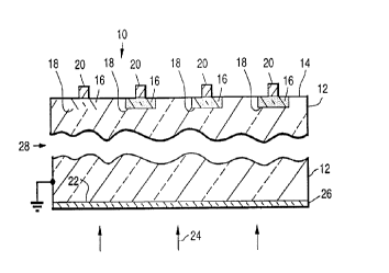
FIG. 1 is a simplified sectional view of a photodetector device
including a photosensitive structure embodying the present invention; and
FIG. 2 is a graph illustrating the relative response per photon of the
present photodetector device.
DETAILED DESCRIPTION OF THE INVENTION
As illustrated in FIG. 1, an InSb photodetector device embodying the
present invention is generally designated as 10, and includes an InSb wafer or
substrate 12 having a front surface 14 in which at least one photosensitive
semiconductor junction is formed. The substrate 12 is typically lightly doped
with an N type dopant such as tellurium. Heavily doped P+ type regions 16
are formed in the surface 14 through ion implantation of beryllium.
Photosensitive semiconductor junctions 18 which constitute photodiodes are
formed at the interfaces of the P+ regions 16 and the N-type substrate 12.
Ohmic contracts 20 are formed on the P+ region 16. A complete circuit
path for the photodiodes is provided by means which are symbolically
indicated by connection of the substrate 12 to ground.
The substrate 12 has a back-side or light receiving back surface 22
which is designated to receive incident light for detection by the device 10
as
indicated by arrows 24. The substrate 12 is thin enough (approximately 8 -12
micrometers thick) for the photogenerated carriers to diffuse therethrough
from beneath the surface 22 to the junctions 18 and cause carrier collection
at
the junctions
4~~
~1 ~14,3~
18.
f
During the fabrication process of the device 10, the
surface 22 is thoroughly cleaned to remove a11 native
oxides of indium and antimony therefrom. A passivation
5 layer 26 is formed on the back surface 22 of a material
which will not react with indium antimonide (InSb) to form
either native oxides or any other substance or structure
which would have carrier traps therein and cause flashing.
The passivation layer 26 is preferably formed of an
l0 silicon oxide and/or nitride material, although the scope
of the invention is not so limited. The passivation layer
26 may be formed of any material which will not produce
carrier traps when formed on the surface 22, will passivate
the surface 22 by preventing reaction thereof with the
ambient atmosphere, and is substantially transparent to
infrared, visible and ultraviolet light in a continuous
spectral range.
For the purposes of the present disclosure, the term
"substantially transparent" means that the passivation
' 20 layer 26 is sufficiently transparent to light within the
selected wavelength range to enable the device l0 to
provide useful operation. Although not illustrated, the
scope of the invention further includes forming an anti.-
reflection coating over the passivation layer 26 of a
' 25 material which is also substantially transparent to light
in the selected wavelength range.
The passivation layer 26 may be formed using a
conventional plasma deposition technique. The preferred
materials for the layer 26 are silicon dioxide .~Si02),
30 silicon suboxide (SiOy) where 0 <_ y _< 2, silicon nitride
i
(Si3N4) or a combination or mixture thereof. The generic
composition of these materials is SiXOyNz, where x = 1 or
3,
0 < y <_ 2 and z = 0 , 1 or 4 .
FIG. 2 illustrates the performance of the present
35 photodetector device 10. The quantum efficiency of the
1
2141~3~
6
f
device 10 in terms of the relative photoresponse per photon
is~plotted as a function of wavelength. A reference level
as indicated by a broken line 30 corresponds to a quantum
efficiency of 0.63 at a wavelength of 4.0 micrometers. It
will be seen that the range of useful photoresponse extends
continuously from approximately 0.3 - 5.5 micrometers,
including the near ultraviolet (UV), visible, short wave
infrared (SWIR) and medium wave infrared (MWIR) spectral
regions.
The data for wavelengths shorter than 1.0 micrometer
was taken with a Cary 14 spectrometer using a quartz-
halogen light source. The data for wavelengths longer than
1.0 micrometer was taken with a Perkin-Elmer 13U prism
monochromator. A discontinuity of approximately 10~ exists
at the 1.0 micrometer interface. However, the data is
sufficiently accurate to demonstrate the useful photore
sponse of the present device 10 in the infrared, visible
~iilat:~::
and ultraviolet spectral regions.
~20 EXAMPLE
Experimental photodetector devices which produced the
results illustrated in FIG. 2 were fabricated using the
following procedure.
' 25 (1) The P+ regions 16, contacts 20, and other
associated elements were formed in the front side 14 of an
InSb substrate or wafer 12 which was initially 750 microme-
ters thick to form operative photodiode junctions 18.
(2) The back side 22 was abraded until the thickness
30 of the substrate 12 was reduced to approximately 15
micrometers.
(3) The front side 14 of the substrate 12 was mounted
on a sapphire slide, and areas of the.back side 22 exce.~t
on which the passivation layer 26 was to be formed were
35 protected with a thick coating of photoresist.
2141034
7
E
(4) The surface 22 was plasma ashed using oxygen
plasma for 10 minutes at a pressure of 0.5 Torr and power
of 150 W.
(5) The surface 22 was chemically etched using a two
step process.
(a) 30 seconds in a 50/50 solution of hydrochlo-
ric acid/de-ionized water. -
(b) 3 minutes in a 70/10 solution of lactic
acid/nitric acid.
Steps (4) and (5) in combination cleaned the back
surface 22 by removing the native oxides, crystal damage
caused by the thinning process in step (2), and some of the
InSb material, such that the final thickness of the
substrate 12 was between approximately 8 to 12 micrometers.
(6) The substrate 12 was rinsed in a de-ionized water
bath, and dried by NZ gas flow. The following step of
applying the passivation layer 26 was perfonued within a
sufficiently short length of time that no appreciable
native oxides were able to form on the surface 22 through
f20 exposure to the ambient atmosphere.
(7) The passivation layer 26 was formed on the
surface 22 of the substrate 12 using conventional plasma
deposition., The passivation layer 26 was a mixture of SiOi
and Si3N4 and was formed from a plasma including N2, 02, and
' 25 silane (SiH4) .
While an illustrative embodiment of the invention has
been shown and described, numerous variations and alternate
embodiments will occur to those skilled in the art, without
departing from the spirit and scope of the invention:
30 For example, although the embodiment of the invention
as described and illustrated includes an indium antimonide
substrate and a silicon oxide or nitride passivation layer,
the scope of the invention encompasses the use of other
substrate materials such as mercury cadmium telluride
35 (HgCdTe), as well as other materials for the passivation
z1~1~~4
8
f
layer.
Accordingly, it is intended that the present invention
not be limited solely to the specifically described
illustrative embodiment. Various modifications are
contemplated and can be made without departing from the
spirit and scope of the invention as defined by the
appended claims.
t