Note: Descriptions are shown in the official language in which they were submitted.
G E02512
SYSTEM AND METHOD FOR IDENTIFYING AN ARRIVAL TIME
OF A COMMUNICATED SIGNAL
TECHNICAL FIELD OF THE INVENTION
The present invention relates generally to an electronic
system that identifies when communicated signals arrive at a
receiving apparatus. In addition, the present invention relates to
1 0 systems which convey communicated signals that are encoded
with pseudorandom noise (PN) sequences.
BACKGROUND OF THE INVENTION
A variety of electronic systems need to identify a precise
point in time when a signal arrives at a receiver. Such systems
include multilateration location determination systems, time
domain reflectometry systems, and the like. '~llhen such systems
calculate distances from the receiver based upon the times of
2 0 arrival for electronic signals traveling at or near the speed of
light, an error of as little as a few nanoseconds in identifying the
precise arrival time can lead to a distance error of over a meter.
A common problem faced by these and other systems is that
of distinguishing a legitimate signal from noise while
simultaneously distinguishing a legitimate signal from multipath
and other corrupting signals. Conventionally, the receiver
generates a detection signal that is compared against a threshold.
A time of arrival is indicated when the detection signal exceeds
the threshold. However, the threshold must conventionally be
3 0 established at a level well above a noise floor to prevent the
system from falsely indicating time of arrivals in response to
noise.
Unfortunately, as the threshold increases, the indicated
time of arrivals become prone to errors resulting from multipath
and other factors. Multipathing results when the signals reach
the receiver by an indirect or reflected path, and often by two or
more paths. Direct path and multipath signals reach a receiver at
different times, but these different signals may coincide to some
CA 02141224 2004-09-23
2
extent. In other words, a leading edge of a multipath signal may
arrive soon after a leading edge of a direct path signal, and then
both are present simultaneously.
Direct path and multipath signals may add to one another or
subtract from one another in the receiver so that time of arrivals
determined through correspondence with the threshold are
inconsistent from situation to situation. If direct path and
multipath signals do not interfere or add together in the receiver,
then a leading edge slope of a detection signal may increase so
that the detection signal actually crosses the threshold correctly.
If direct path and multipath signal subtract from one another in
the receiver, the detection signal may fail to reach the threshold
or reach the threshold too slow.
The use of spread spectrum communication signals helps
1 5 the multipath .problem to some degree. Spread spectrum signals
are encoded with a pseudorandom noise (PN) spreading sequence,
or code. A correlator in a receiver generates a distinctive, high
amplitude detection signal during a period in time while the
communication signal correlates with the PN sequence. Multipath
signals which arrive at the receiver after this period in time
have little or no influence. However, this period may last for
many tens of nanoseconds, and multipath signals arriving during
this period can still corrupt the detection signal.
2 5 SUMMARY OF THE INVENTION
The present invention seeks to overcome the disadvantages of the prior art
associated with system and method for identifying an arrival time of a
communicated
3 0 signal.
According to one aspect of the invention, an apparatus for identifying an
arrival time of a communicated signal which conveys a message having a
plurality of
bits of data is provided. The apparatus comprises: a correlator for
correlating the
communicated signal with a psendorandom noise (PN) sequence and to generate a
CA 02141224 2004-09-23
2A
correlation signal; means, coupled to the correlator, for detecting the
occurrence of a
fiirst bit of the message; and means, coupled to the detecting means and to
the
correlator, for determining when, after the first bit, the correlation signal
corresponds
to a threshold, wherein the determining means comprises a comparison circuit
which
is disabled during the first bit.
According to another aspect of the invention, a method of identifying an
arrival
time of a communicated signal which conveys a message having a plurality of
bits of
data is provided. The method comprises the steps of: initiating a clock to
mark the
passage of time; establishing a threshold; receiving first and second bits of
the
signal: correlating the first and second bits of the signal with a PN
sequence, the
correlating step producing a correlation signal; and stopping the clock
following the
first bit at a point in time when the correlation signal corresponds to the
threshold,
wherein the stopping step occurs during the second bit.
According to another aspect of the invention, a system for identifying an
arrival time of a communicated signal is provided. The system comprises: a
spread
spectrum transmitter configured to transmit the communicated signal, the
communicated signal conveying a message having a plurality of bits, the bits
exhibiting first or second states wherein the first state is conveyed by
encoding the
communicated signal with a PN sequence and the second state is conveyed by an
absence of PN sequence encoding in the communicated signal; means for
receiving
the communicated signal: a correlator coupled to the receiving means, the
correlator
being configured to correlate the communicated signal with the PN sequence and
to
generate a correlation signal; means, coupled to the correlator, for detecting
the
occurrence of a first one of the bits of the message; and means; coupled to
the
detecting means and to the correlator, for determining when, after the first
bit, the
correlation signal corresponds to a threshold, wherein the determining means
comprises: a comparison circuit configured to compare the correlation signal
with the
threshold; and means, coupled to the comparison circuit, for disabling the
comparison circuit during the first one of the bits and for enabling the
comparison
circuit during a second one of the bits, the second one of the bits occurring
immediately after the first one of the bits.
CA 02141224 2004-09-23
2B
The "Summary of the Invention" does not necessarily disclose all the inventive
features. The inventions may reside in a sub-combination of the disclosed
features.
BRIEF DESCRIPTION OF THE DRAWINGS
A more complete understanding of the present invention .
may be derived by referring to the detailed description and claims
when considered in connection with the Figures, wherein like
reference numbers refer to similar items throughout the Figures,
and:
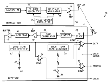
FIG. 1 shows a block diagram of a first portion of a system
configured in accordance with the teaching of the present
invention;
FIG. 2 shows a timing diagram that depicts some of the
signals generated by components of the system; and
3
FIG. 3 shows a block diagram of a second portion of the
system.
DETAILED DESCRIPTION OF THE PREFERRED EMBODIMENTS
FIG. 1 shows a block diagram of a first portion of a system
configured in accordance with the teaching of the present
invention. System 10 identifies the arrival time of a signal that
has been communicated from a transmitter 1 ~'. and is being
10 received at a receiver 14. In the preferred embodiment, system
10 is used by a multilateration location system in which the
location of transmitter 12 is determined relative to known-
positions of several of receivers 14, each of which is configured
like the others. However, system 10 is not limited to being used
1 5 only in a location determination system. System 10 may be used
in connection with a variety of electronic systems where the
arrival time of a communicated signal at a receiver is identified
to a high degree of precision.
Transmitter 12 is configured to generate and broadcast a
2 0 spread spectrum signal. This communicated signal conveys a
digital message 16, as illustrated in the timing diagram shown in
FIG. 2. As shown in FIG. 2, message 16 may include any number of
bits 18 of data. FIG. 2 illustrates a portion of the data stream
containing the first through fifth bits 18. In the preferred
2 5 embodiment, the duration of message 16 and the duration of bits
18 within message 16 are relatively constant from message to
message. The precise value of these durations is not important to
the present invention.
Referring to FIGs. 1 and 2, a controller 20 generates
30 message 16. Controller 20 may include a microprocessor,
memory, and related components conventionally found in
transmitters. The precise makeup of message 16 is, for the most
part, not a critical feature of the present invention. However,
controller 20 configures message 16 so that at least two
35 consecutive bits 18 at a consistent location in message 16
exhibit the same state, which is preferably a Vogical one. This is
4
accomplished by configuring message 16 to include a preamble
having logical values of 1-1-0 for the first bit, second bit, and
third bit of FIG. 2 bits 18.
Controller 20 serially feeds message 16 to a PN code
generator 22. A phase-locked oscillator 24 couples to both PN
code generator 22 and a bi-phase modulator 26. An output of
modulator 26 couples to an RF amplifier 28, and amplifier 28
drives an antenna 30. In the preferred embodiment, generator 22
encodes message 16 with a predetermined maximal length, 127
1 0 bit PN sequence.
More particularly, generator 22 produces the PN sequence
only during the bits 18 of message 16 that exhibit one state,
which is a logical one in the preferred embodiment. As shown in
FIG. 2, the first and second bits of bits 18 convey the PN
1 5 sequence. During bits 18 that exhibit the other state, a logical
zero in the preferred embodiment, PN code generator 22 produces
no code, as shown in the third bit of bits 18 in FIG. 2.
Accordingly, for each logical one bit 18 conveyed by message 16,
a communicated signal broadcast from antenna 30 is bi-phase
2 0 modulated to convey the PN sequence. For each logical zero bit 18
conveyed by message 16, the communicated signal broadcast from
antenna 30 conveys nothing, or silence.
Receiver 14 is configured for compatibility with the
communicated signal broadcast by transmitter 12. While FIG. 1
25 illustrates only one receiver 14, system 10 may include any
number of receivers 14, and more than one of these receivers 14
may receive the communicated signal. The communicated signal
will arrive at the receivers 14 at different times depending upon
the relative distances between the receivers 14 and the
30 transmitter 12. By identifying the times at which the
communicated signal arrives at the different receivers 14, a
multilateration location process may resolve a position for
transmitter 12. The precision of the resolved position will be
depend upon the precision with which the receivers 14 identify
35 the times at which the communicated signal arrives. While the
following discussion is directed toward a single receiver 14,
~~.~~1~24
those skilled in the art will appreciate that it may apply to
multiple receivers 14 as well.
Receiver 14 includes an antenna 32, which couples to an RF
stage 34. The communicated signal is received at antenna 32 and
5 converted to an IF signal through RF stage 34. RF stage 34
couples to a limiter 36, which removes a large portion of
amplitude variation from the bi-phase communicated signal,
leaving the signal's frequency content. Limiter 36 couples to a
surface acoustic wave (SAW) correlator 38.
1 0 Correlator 38 is formed so that the predetermined PN
sequence discussed above in connection with PN code generator
22 is preprogrammed therein. Accordingly, correlator 38 is used
to perform a correlation function upon the communicated signal.
When correlator 38 is loaded with a communicated signal
1 5 conveying the PN sequence, correlation results. During the
correlation, correlator 38 generates a large amplitude output.
However, under other circumstances correlator 38 generates a
smaller amplitude output. Correlator 38 couples to an IF
amplifier 40, which amplifies the output signal from correlator
20 38. An output of IF amplifier 40 couples to a detector 42, which
performs an absolute value and filtering operation on the signal.
An output of detector 42 couples to a buffer amplifier 44, which
provides amplification and impedance matching for subsequent
operations. The output of buffer 44 generates a correlation
2 5 signal 46, an example of which is shown in the bottom trace of
FIG. 2.
The preferred embodiment of the present invention exploits
the nature of PN sequences and SAW correlator 38 to control the
behavior of correlation signal 46. So long as correlator 38 is
30 entirely loaded with its PN sequence, even though it is not
correlating, it generates less noise than it generates when loaded
with random noise or other signals. In theory, for a maximal
length 127 bit code the time sidelobes generated by correlator 38
should be around 42 dB below a peak amplitude achieved during
3 5 correlation. However, in practice this value does not achieve the
42 dB attenuation due to manufacturing imperfections.
%~.~~_'~?~
s
Nevertheless, the time sidelobe output produced by correlator 38
when a currently received bit 18 and an immediately previous bit
18 convey the PN sequence are less than the output produced by
correlator 38 when it is not preloaded with the PN sequence from
the immediately previous bit 18.
FIG. 2 graphically illustrates this phenomenon. Spikes or
peaks 48 of correlation signal 46 occur when correlator 38 is
completely loaded and correlates with its PN sequence. Prior to
the end of the third bit of bits 18, correlator 38 was loaded with
random noise. During this prior period, corrE~lation signal 46
exhibited a generally high level, as illustrated during interval 50.
This generally high noise level decreases as more of the PN
sequence loads into correlator 38. After correlation for the
fourth bit 18, the fourth bit's PN sequence exits correlator 38 as
1 5 the fifth bit's PN sequence loads. Thus, during the fifth bit,
which occurs after spike 48 for the fourth bit, the noise level of
correlation signal 46 is relatively low because correlator 38 has
been preloaded with its PN sequence. This is shown in FIG. 2 as
the low amplitude of correlation signal 46 after spike 48 at the
2 0 end of the fourth bit.
Referring back to FIG. 1, buffer 44 couples to inputs of a
long term peak detector 52, an event comparison circuit 54, a
short term peak detector 56, a data comparison circuit 58, and a
timing comparison circuit 60. An output of long term peak
2 5 detector 52 couples through a resistor divider chain 62 to a
ground node 64. An intermediate node of resistor divider chain 62
couples to an input of event comparison circuit 54. Likewise, an
output of short term peak detector 56 couples through a resistor
divider chain 66 to ground node 64. A first intermediate node of
3 0 resistor divider chain 66 couples to an input of data comparison
circuit 58, and a second intermediate node of resistor divider
chain 66 couples to an input of timing comparison circuit 60.
Long term peak detector 52 is configured to sample the peak
level of correlation signal 46 (see FIG. 2) and to hold this peak
35 level for a long term, which is on the order of 2-5 seconds in the
preferred embodiment. Resistor divider chain 62 is configured so
7
that the intermediate output establishes an Event threshold 68
which is around 1 /2 of this peak value. FIG. 2 depicts event
threshold 68 as a dotted line shown in relation to correlation
signal 46. Consequently, event comparison circuit 54 finds
correspondence with event threshold 68 whenever the
instantaneous value of correlation signal 46 exceeds about 1/2 of
the peak signal level achieved by correlation signal 46 over a
previous predetermined duration of more than a couple of seconds.
By finding correspondence with a threshold, such as event
threshold 68 or other thresholds discussed below, those skilled in
the art will understand that such correspondence may result from
either exceeding the threshold or falling below the threshold. For
example, in alternate embodiments of the present invention,
polarities may be reversed so that comparison circuits find
1 5 correspondence when a signal falls below a threshold.
Event comparison circuit 54 detects the occurrence of the
first one of bits 18 from message 16. Subsequent logical one bits
are also detected, but this is of little consequence in the
preferred embodiment of the present invention. Long term peak
detector 52 provides a mechanism so that this detection self-
compensates for false alarms.
As discussed below, the detection of the first bit 18 of
message 16 starts a chain of events that continues for longer
than the duration of message 16. If event threshold 68 is set too
2 5 low, event comparison circuit 54 may trigger on noise, and the
chain of events will then commence and possibly prevent
legitimate messages 16 from being recognized. If event
threshold 68 is set too high, event comparison circuit 54 may fail
to trigger on weaker correlation signals 46. Thus, if receiver 14
3 0 fails to detect events for a long term period, event threshold 68
begins to droop so that weaker and weaker correlation signals 46
will be recognized as events. The chances of falsely triggering on
noise increase, but since receiver 14 is not detecting many
events the chances of a false trigger preventing legitimate
35 messages 16 from being recognized are low ire this situation. On
the other hand, if receiver 14 is detecting many events, then
1 ;~ ~.,Wl~
8
event threshold 68 remains high so that the likelihood of falsely
triggering on noise is reduced and the chances of legitimate
messages 16 not being recognized are likewise low.
Short term peak detector 56 is configured to quickly sample
the peak level of correlation signal 46 (see FIG. 2) and to hold
this peak level for only a short term, which is slightly longer
than the duration of message 16 in the preferred embodiment.
Resistor divider chain 66 establishes a data threshold 70, which
is shown in FIG. 2, at the first intermediate output and a timing
1 0 threshold 72, which is also shown in FIG. 2, at the second
intermediate output. Desirably, data threshold 70 is set at
slightly greater than 1/2 the peak value while timing threshold
72 is set at less than 1 /2 the peak value. More preferably, data
threshold 70 is set at around 5 dB below the peak value and
1 5 timing threshold 72 is set at around 12 dB below the peak value
in the preferred embodiment.
Data comparison circuit 58 detects correspondence between
the instantaneous value of correlation signal 46 and data
threshold 70. When correspondence is detected, a logical one may
2 0 be recovered from the communicated signal. 'When
correspondence is not detected at an appropriate time, a logical
zero may be recovered from the communicated signal. Timing
comparison circuit 60 detects correspondence between the
instantaneous value of correlation signal 46 and timing threshold
25 72. When correspondence is detected, time may be measured to
identify when the communicated signal arrives at receiver 14.
As discussed above, the noise level of correlation signal 46
increases, as shown at interval 50 in FIG. 2, when correlator 38
has not been preloaded with its PN sequence. Moreover,
3 0 correlator 38 is not preloaded with its PN sequence when either
the current or previous bit 18 is a logical zero. Thus, data
threshold 70 is set at a higher level so that the chances of
finding correspondence with noise are very low while the chances
of finding correspondence with a legitimate spike 48 (see FIG. 2)
3 5 are very high.
On the other hand, timing threshold 72 is set at a lower
~~.4.Z~~~
s
level so that correspondence will be found as soon as possible
relative to the leading edge of the spike 48 that results from the
second bit of bits 18 in message 16, as illustrated at point in
time 74 in FIG. 2. The lower the timing threshold 72 the better
because the influence of multipath is minimized. If multipath and
direct path communicated signals tend to subtract from one
another at receiver 14, then the combined correlation signal 46
may exhibit a more gradual slope than results from the direct
path signal alone. A higher value timing threshold 72 would
1 0 magnify the effects of the more gradual slope and provide a
greater timing error. In addition, since the noise level of
correlation signal 46 is lower during the second bit 18 of
message 16 than it may be at other times in message 16, the low
value for timing threshold 72 does not significantly risk false
triggering on noise.
The event, data, and timing thresholds against which the
instantaneous value of correlation signal 46 is compared are
determined in response to peak values for correlation signal 46
rather than in response to a noise floor. This implementation is
desirable because it provides greater immunity from noise. In
particular, receiver 14 need not be configured to operate in
accordance with worst case noise considerations. In addition, a
more consistent and robust performance is obtained because the
signal peaks and not the noise floor convey the information
2 5 gathered by receiver 14.
An event clock signal 76, for which a timing diagram is
shown in FIG. 2, drives enable inputs of comparison circuits 58
and 60. When event clock signal 76 is inactive, which is depicted
as a low level in FIG. 2, comparison circuits 58 and 60 are
prevented from finding correspondence. In the preferred
embodiment, comparison circuits 58 and 60 have separate data
and timing event clocks. As shown in FIG. 2, event clock signal 76
is inactive until after a previous spike 48 (not shown) from the
first bit crosses the event threshold 68 in message 16. Thus,
through event clock signal 76, comparison circuits 58 and 60 are
prevented from finding correspondence during the first bit of
~1.~~~~~'~
message 16.
FIG. 3 shows a block diagram of a control section 78 of
receiver 14. As shown in FIG. 3, a control logic block 80 of
control section 78 generates event clock signal 76. Control logic
5 block 80 uses conventional counter circuits (not shown) to
generate event clock signal 76 in response to the activation of an
event signal. The event signal activates when event comparison
circuit 54 (see FIG. 1 ) detects the first bit of message 16 (not
shown in FIG. 2). Generally speaking, event clock signal 76
1 0 activates prior to the end of each bit 18 in message 16, except
for the first bit 18. Event clock signal 76 remains active into the
beginning of the next bit 18. Thus, event clock signal 76 will be
active if a spike 48 occurs due to the conveyance of a logical one
bit in message 16.
1 5 Data comparison circuit 58 (see FIG. 1 ) generates a data
signal that sets a flip flop 82 when correspondence with data
threshold 70 (see FIG. 2) is found. Event clock signal 76 or its
inverse drives a reset input of flip flop 82 so that flip flop 82
resets when event clock signal 76 is inactive. An output of flip
flop 82 couples to a data input of a shift register 84, and the
event clock signal 76 or its inverse also drives a clock input of
shift register 84. Polarities are arranged sc~ that shift register
84 clocks as event clock signal 76 goes inactive.
Flip flop 82 and shift register 84 recover data, other than
the first bit of message 16, from the communicated signal. The
flip flop 82 storage element is reset prior to the general timing
interval where a spike 48 (see FIG. 2) might be present. Flip flop
82 is then set when a logical one data bit 18 causes a spike 48
(see FIG. 2). Flip flop 82 is not set and remains in its reset state
3 0 when logical zero data bit 18 occurs. The state of flip flop 82 is
shifted into the shift register 84 storage element after each bit
i 8 in message 16.
Timing comparison circuit 60 (see FIG. 'I ) generates a
timing signal that resets a flip flop 86 when correspondence with
data threshold 72 (see FIG. 2) is found. An output of flip flop 86
couples to an enable input of a high speed counter clock 88 and to
11
a first input of a logic gate 90. Polarities are arranged so that
counter clock 88 refrains from counting when flip flop 86 is
reset, and flip flop 86 resets as soon as timing comparison
circuit 60 (see FIG. 1 ) finds correspondence with timing threshold
72. Flip flop 86 remains reset throughout the remainder of
message 16, and counter clock 88 is prevented from counting
throughout the remainder of message 16.
A high speed clock signal, that in the preferred embodiment
oscillates at almost 1 GHz, drives a master clock 92 and a clock
1 0 input of high speed counter clock 88. Due to 'the high speed of the
high speed clock signal, all or at least the faster stages of clocks
88 and 92 are implemented using an appropriate digital circuit
technology, such as ECL. However, slower stages may be
implemented using CMOS or other less expensive and complex
digital circuit technologies. Master clock 92 and high speed
counter clock 88 represent counter circuits. An output, such as a
terminal count output, of clock 92 couples to a second input of
logic gate 90. However, master clock 92 may serve as a master
clock for multiple ones of receivers 14 and not just a single
2 0 receiver 14 as shown in FIG. 3.
Master clock 92 and logic gate 90 provide a synchronizing
function for counter clock 88. Logic functionality and signal
polarities surrounding logic gate 90 are arranged so that counter
clock 88 synchronizes with master clock 92 from time to time by
2 5 being cleared, loaded with a predetermined value, or the like.
More particularly, synchronization occurs when flip flop 86 has
enabled counter clock 88 and master clock 92. reaches a terminal
count.
Once initialized or synchronized with master clock 92, high
3 0 speed counter clock 88 marks the passage of time in a manner
that is consistent with master clock 92. Counter clock 88 counts
oscillations of the high speed clock signal until disabled by flip
flop 86. Counter clock 88 becomes disabled when correlation
signal 46 (see FIG. 2) corresponds to timing threshold 72 (see FIG.
35 2). Counter clock 88 remains disabled throughout the remainder
of message 16 so that the count achieved at the moment of being
12
disabled does not change.
Control logic block 80 couples to a computer 94, as does
shift register 84 and high speed counter clock 88. After the
end of message 16, control logic 80 may inform computer 94 of
the presence of message 16. Computer 94 may then read the data
and timing from shift register 84 and counter clock 88,
respectively. After the data and timing have been read, control
logic 80 is free to activate an end-of-message signal 96, for
which a timing diagram is shown in FIG. 2. Fnd-of-message
1 0 signal 96 drives a set input of flip flop 86. By setting flip flop
86 after data and timing have been read, counter clock 88 again
becomes enabled to count. Then, after a predetermined period of
time counter clock 88 becomes synchronized with master clock
92.
1 5 Computer 94 may use the data and timing information in any
manner which is useful to system 10 (see FIG. 1 ). For example,
computer 94 may subtract the duration of onE: bit 18 from the
timing data measured by counter clock 88 to determine the time
of arrival of the initial bit of message 16. Alternatively,
2 0 computer 94 may simply compare different times of arrival
measured from different receivers 14 in a conventional manner
while performing a multilateration location process.
In summary, the present invention provides an improved
system for identifying an arrival time of a communicated signal.
2 5 A spread spectrum communicated signal is used to reduce the
corrupting influences of multipath. These corrupting influences
are further reduced by determining time of arrival in
correspondence with a low timing threshold. The preferred
embodiments of the present invention identify a point in time
30 during the transmission of a message when noise on a correlation
signal will be reduced to lessen the chances of falsely indicating
a time of arrival in response to noise. Furthermore, the
thresholds against which the detection signal is compared are
determined in response to peak values of they correlation signal
35 rather than in response to a noise floor.
The present invention has been described above with
13
reference to preferred embodiments. However, thaw skilled in
the art will recognize that changes and modifications may be
made in these preferred embodiments without departing from the
scope of the present invention. For example, different signals
could be used to enable data and timing comparison circuits with
different timing. Moreover, different logic could be used to
recover data and timing data from the data and timing comparison
circuits. In addition, not all features described above need be
included in a workable system that incorporates the present
1 0 invention. For example, the variable event threshold discussed
above may be replaced by a constant predetermined value with
only slight degradatian in performance. These and other changes
and modifications which are obvious to those skilled in the art
are intended to be included within the scope of the present
invention.