Note: Descriptions are shown in the official language in which they were submitted.
21 41379 Lerminiaux - 5
RRn~nR~ND INTEGRATED OPTICAL PPOYTMTTY COUPLER
R~ckgrolln~ of the Tnvent;on
The present invention relates to an optical device for
proximity coupling between two waveguides integrated in a
substrate, and more particularly, to such a device which is
characterized by low loss, broadbanded operation and which
possesses acceptable cutoff wavelength characteristics.
Cost reductions in optical networks can be obtained by
sharing the fiber among multiple subscribers. The ion-
exchange technique, for example, has proved to be a
promising technology for producing lxN splitters with
output ports numbering as high as 16. Such devices, when
formed as Y junctions, provide excellent achromaticity and
uniformity at low loss.
The ability to provide a second input to a system is
becoming more desirable for various reasons such as (a) the
multiplexing of two different signals; (b) redundancy in
different paths to reach a splitting point; (c) flexibility
in the future deployment of the network; and (d) providing
a network testing entry point. Junctions which can provide
a second input, a 2x2 junction, for example, are more
difficult to realize than a lx2 junction, when using planar
Y junction technology. The combination of two Y junctions,
one to provide a second input to a lxN splitter, results in
a 3 dB additional loss; such high loss is unacceptable.
Therefore, interferometric devices have been employed
for combining signals in integrated circuits. Fig. 1 shows
2141379
~ .
--2--
a symmetrical waveguide coupler 10 which functions as a
wavelength division multiplexer (WDM) for the
combining/separating of two signals of different
wavelengths. It comprises two straight parallel waveguides
11 and 12 and curved approach segments 13, 14, 15 and 16,
the ends of which are referred to as input/output ports.
The ports are separated by a distance fixed by the diameter
of coated optical fibers 19-22 which are attached to these
ports by a technique of "pigtailing", for example.
A broadbanded optical waveguide coupler is disclosed
in the publication, A. Takagi et al. "Broadband Silica-
Based Optical Waveguide Coupler with Asymmetric Structure",
Electronics Letters, 18 Jan. 1990, Vol 26, No. 2, pp. 132-
133. The device is made broadbanded by forming the two
paths such that they have different propagation constants
in the coupling region. Referring to Fig. 1, propagation
constants are made different by changing the width of one
of the waveguide paths. Straight waveguide 11 and segments
13 and 15 remain the same width as they were in the WDM
coupler, but waveguide 12' is narrower than waveguide 11,
approach segments 14 and 16 being tapered from standard
width at the input and output ports to the narrower width
at waveguide 12'.
In a ~ proximity coupler the power transferred from
one waveguide to the other is given by
Pl2=P sln~
where L is the length of the interaction, C is the coupling
constant, and F depends upon a~, the difference between the
propagation constants ~1 and ~2 of the two waveguides, and
is given by
Z141379
-3
~ )2 ~ ~2)
In order to make a 3 dB coupler, it can be shown that the
wavelength response of the proximity coupler is flattened
to a maximum extent when F2 equals ~ and L is chosen in
such a way that CL/F equals (2n+1)~/2. Incomplete power
transfer occurs, whereby output power as a function of
wavelength is flatter.
The ~ coupler of the Takagi et al. publication is
formed by a combination of flame hydrolysis deposition of
sio2 on Si, photolithography, and reactive ion etching. A
relatively small excess loss is induced in the curved
portions of the narrowed approach segments 14' and 16'
because of their reduced diameter.
The ion-exchange process is different from flame
hydrolysis or other planar techniques in that it is
impossible to reduce the width of an ion-exchange waveguide
path without reducing its maximum index of refraction.
Therefore the effective index of the narrower path is
reduced by both (a) the narrowing of the path width and (b)
the diminution of the refractive index. When ion-exchange
technology is used to form the waveguide paths in a ~
proximity coupler, both effects (a) and (b) will increase
the effective index difference between the two paths (and
thus the ~), and both effects will also increase the
losses in the bend approach region.
Summary of the Invention
It is therefore an object of the present invention to
provide an improved integrated optical proximity coupler.
A further object is to provide a broadbanded integrated
optical proximity coupler that exhibits low loss and
exhibits desired cutoff wavelength properties.
Briefly, the present invention relates to an
', 21gl~9
integrated optical device for proximity coupling between
two waveguides. The device comprises first and second
waveguide input end segments having the same width. First
and second straight interaction waveguide segments are
parallel and near to one another. The first straight
segment is narrower than the first and second input end
segments, and the second straight segment is wider than the
first and second input end segments. The spacing between
the first and second straight interaction segments is less
than the spacing between the first and second input end
segments. First input means connects the first input end
segment to the first straight segment, and second input
means connects the second end segment to the second
straight segment. Output means couples a signal from one
of the first and second straight paths.
Rri ef Description of the ~r~w;ngs
Fig. 1 is a schematic illustration of a prior art
asymmetric integrated optical proximity coupler.
Fig. 2 is a schematic illustration of an asymmetric
integrated optical proximity coupler formed in accordance
with the present invention.
Figs. 3 and 4 are schematic illustrations of two
different modifications of the output end of the device of
Fig. 2.
Fig. 5 is a graph showing insertion loss plotted as a
function of wavelength.
Descript;on of the Preferre~ Emkodiments
The drawings are not intended to indicate scale or
relative proportions of the elements shown therein.
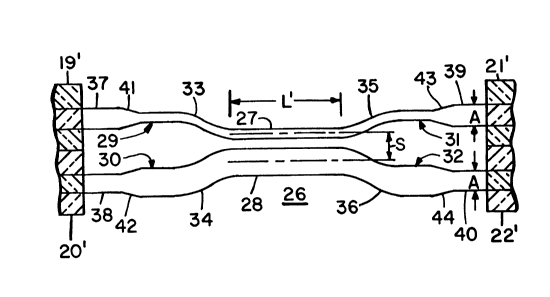
The improved ~ coupler 26 of the present invention is
shown in Fig. 2. The coupler comprises two straight
parallel waveguides 27 and 28 and approach segments 29, 30,
31 and 32. Approach segments 29 and 31, which are
` 2141379
,
--5--
connected to straight segment 27, comprise curved segments
33 and 35, respectively, which are connected to end
segments 37 and 39, respectively, by transition segments 41
and 43, respectively. Approach segments 30 and 32, which
are connected to straight segment 28, comprise curved
segments 34 and 36, respectively, which are connected to
end segments 38 and 40, respectively, by transition
segments 42 and 44, respectively. The transition segments
are needed to provide low loss connections between the
waveguide paths of the coupler to optical fibers. Whereas
the transition segments are located immediately adjacent
the end segments in Fig. 2, they could be located along the
lengths of the curved segments as shown in Fig. 1.
However, locating a transition segment in a curved region
can increase loss.
Straight waveguide segment 27 is narrower than end
segments 37 and 39. To reduce excess loss, narrower path
27 is not made quite as narrow as it was in the prior art
(see Fig. 1). This is accomplished by making the other
straight waveguide path 28 slightly wider than end segments
38 and 40. Thus, the required ~ can be achieved without
making path 27 so narrow that its width and reduced
refractive index excessively increase excess loss.
As the width of straight segment 28 increases, its
cutoff wavelength increases. The standard cutoff
wavelength of the second mode is around 1200 nm. A 1.0 ~m
difference in path width will result in a 200 nm shift in
cutoff wavelength. The wider path 28 cannot be not made so
wide that it's cutoff wavelength exceeds the wavelength of
operation, since some noise or losses due to the injection
of power into the second order mode is possible. The
difference between the propagation constants of the two
coupled waveguides is therefore obtained by a reasonable
change in width of both waveguides, as compared to a
standard narrow band coupler having straight paths of equal
widths.
If the end segments have a path width between about 2
- 2141 ~79
.. ..
- ~m and 4 ~m, segments 27 and 28 will normally differ in
width from the end segment width by about 0.2 ~m to 0.5 ~m.
For ~ couplers made in accordance with this
invention, S' is typically between 9 ~m and 12 ~m, and L'
is between 500 ~m and 2000 ~m to have 3dB splitting ratio
at 1.3 and 1.55 nm. The distance L' is the length of the
coupling region, and S' is the distance from the center of
one waveguide to the center of the other waveguide.
Tapered segments 41-44 have been made as long as 1 mm,
but lengths as short as 100 ~m have performed
satisfactorily. Longer tapers merely unduly lengthen the
device.
In a specific example, the device was constructed by
an ion-exchange process. Examples of methods and apparatus
for forming by ion-exchange an optical waveguide path in
the surface of a glass substrate and the subsequent burying
of that path can be found in US patents Nos. 3,836,348;
4,765,702; 4,842,629; 4,913,717; and 4,933,262. Also see
publications: R.V. Ramaswamy et al. "Ion-Exchanged Glass
Waveguides: A Review", Journal of Lightwave Technology,
Vol. 6, No. 6, June 1988, pp. 984-1002; H.J. Lilienhof et
al. "Index Profiles of Multimode Optical Strip Waveguides
by Field Enhanced Ion Exchange in Glasses", Optics
Communications, Vol. 35, No. 1, October, 1980, pp. 49-53;
and A. Miliou et al. "Fiber-Compatible K+-Na+ Ion-Exchanged
Channel Waveguides: Fabrication and Characterization", IEEE
Journal of Quantum Electronics, Vol. 25, No. 8, August,
1989, pp 1889-1897. The substrate was formed of an
alumino borosilicate glass containing sodium and potassium
ions. Its refractive index was 1.463. The exchanged ion
that formed the waveguide paths was thallium. The width of
the mask apertures for paths 27, 33 and 35 was 2.6 ~m. The
width of the mask apertures for paths 28, 34 and 36 was 3.2
~m. The width of the mask apertures for paths 37, 38, 39
and 40 was 2.9 ~m. There is a direct correlation between
mask aperture width and index profile radius or waveguide
path width. The cross-sectional shape of the high index
2I41379
--7--
waveguide is somewhat circular, the profile being diffused.
The dimensions L' and S' were 1000 ~m and 11.5 ~m,
respectively. Fig. 5 shows the insertion loss for this
coupler. Curve 61 represents the output signal at segment
39 when the input signal is applied at segment 37. Curve
62 represents the output signal at segment 40 when the
input signal is applied at segment 37. Curve 63 represents
the output signal at segment 40 when the input signal is
applied at segment 38. Insertion loss is 3.3 dB + 0.5 dB
in the first window (1260 to 1360 nm) and 3.7 dB + 0.5 dB
in the second window (1480 to 1580 nm). The average excess
loss is therefore of the same level as for a standard WDM
coupler.
If the device is used only for combining two signals,
it need not have an output segment connected to both
straight segments 27 and 28. Examples are shown in Figs. 3
and 4 wherein elements similar to those of Fig. 2 are
represented by primed reference numerals. In Figs. 3 and
Fig. 4, curved segments 36 and 35, respectively, are
replaced by termination segments 50 and 55, respectively.