Note: Descriptions are shown in the official language in which they were submitted.
CA 02141525 2001-O1-29
78626-1
1
SMART SKIN ARRAY WOVEN FIBER OPTIC RIBBON AND ARRAYS AND
PACKAGING THEREOF
CROSS REFERENCE TO RELATED APPLICATION
This application corresponds to now issued U.S.
Patent 5,524,679 which i.s related to United States Patent No.
5,256,468, issued October 26, 1993.
BACKGROUND OF THE INVENTION
This invention. relates to optical systems and optical
fibers, and particularly to optical fibers woven into other
material to provide sensors or "smart" skins for aircraft and
other applications such as optical backplanes for highly
parallel, high performance computer systems, and local area
network interconnects.
Fiber optic technology has become increasingly
desirable for numerous aircraft and spacecraft applications,
and for data transmissior_ in highly parallel, high performance
computer systems, as well as local area network interconnects.
The size, weight, communications density, immunity to
interference, and ruggedness, are pushing fiber optic
technology into more and more applications where it provides
greater speed capabilities and integrity of communication
links.
A recent concept in the manufacture of aircraft and
spacecraft has been the employment of fiber optics within the
skin of the craft itself, thereby creating a "smart" skin which
enables sensors embedded into the composite material to convey
information about the aircraft or spacecraft throughout the
craft without need for separate communication links and their
associated disadvantages.
~_~.~~.5~
2
The mechanical properties of material woven from
glass fibers are reasonably well known. Such material
provides desirable mechanical properties including high
tensile strength, flexibility, resistance to weather as well
as chemicals, high tear strength, dimensional stability, and
abrasion resistance.
It is also known that individual optical fibers
can be used to transmit optical signals throughout the
length of the fiber and have very high bandwidths.
Individual optical fibers have excellent optical properties,
but are very fragile. A variety of techniques have been
developed to hold individual fibers in a manner to prevent
damage to them. For example, they are frequently encased in
cables or other protective material. In addition,
individual fibers can be grouped together to provide cables
capable of carrying increased amounts of information.
One technique widely used for protection of
optical fibers is to encapsulate them in an epoxy material
to provide rigidity and strength. For example, U.S. Patent
No. 4,547,040 describes an optical fiber assembly where
optical fibers are held in an embedding material.
Individual optical fibers have also been woven
into sheets. For example, U.S. Patent No. ,x,907,132
describes a device where optical fibers are woven into a
panel. The fibers are positioned in the warp direction of
the weave. Where the fibers cross the woof fibers, the
coating is removed so that the fibers emit light. In this
manner, a panel made from the fibers emits light. U.S.
Patent No. 4,885,663 shows woven optical fibers where the
0 bends in the fibers where they cross the woof provide
discontinuities for the emission of light. The purpose of
this structure is provide a light-emitting panel.
Other references such as U.S. Patent
Nos. 4,952,020 and 4,468,089 show optical fibers which are
encapsulated in various ways to form cable assemblies such
as described above. Unfortunately, the cable assemblies
described in these patents are relatively expensive and
cannot be used to form sheet-like structures.
2~41.5~~
3
Many papers have been written on the application
of optical fibers to the formation of "smart" skins for
aircraft or spacecraft. In "Fiber Optic Skin and Structural
Sensors," by Eric Udd, Industrial Metrolocty 1 (1990) 3-18,
the use of optical fibers in a skin-like material for use as
sensors is described. The paper, however, describes the
fibers as being merely embedded in a structural material.
Embedding the fibers in that manner suffers from the
disadvantages discussed in the paper discussed below.
In a paper entitled, "Smart Skins and Fiber-optic
Sensors Application and Issues," Kausar Talat, Boeing
Defense & Space Group, Seattle, Washington (unpublished),
describes material with embedded optical fibers where the
physical properties of the fiber itself were used as a
sensor. The composite described in this article includes
optical fibers disposed inside a laminated structure. At
the end of the structure, the optical fibers pass through a
tube inserted to prevent micro-bending of the fiber =where it
exists from between the laminated sheets. As described in
the article, the laminated structure causes the fibers to
kink during curing, creating losses as well as having other
disadvantages discussed in the paper.
SUMMARY OF THE INVENTION
The present invention provides a structure which
solves many of the problems described above. According to
the invention, the optical fibers are woven into a
supporting structure in channels therein. The optical
fibers are positioned in zero warp and supported in the
channels without cross-overs or micro-bends. The term "zero
warp", also known as "zero degree warp", refers to the
manner in which warp threads are positioned in, for example,
a conventional plain weaving process. In such a process,
two sets of fibers are interlaced perpendicular to each
3~ other. One set of fibers, the zero degree warp or zero ~rarp
fibers, are positioned straight and parallel in a direction
perpendicular to the heddle. The other set of fibers, tt~e
2141,52
4
woof fibers, are interlaced with the warp fibers at a ninety
degree angle to the warp fibers.
According to the present invention, optical fibers
are positioned and held in a grid-like mat woven from fibers
of a supporting material. This supporting material can
consist of any desired material providing the requisite
properties, for example, fiberglass, graphite, etc. The
supporting fibers are used for both the warp and woof fibers
for the structure. During manufacture, one or more optical
fibers are positioned in channels between the supporting
fibers in the warp direction. Each channel can have a large
number of optical fibers.
As mentioned above, the structure is woven with
the optical fibers positioned in zero warp. This enables
the optical fibers to be supported in the woven structure,
and thereby to operate with maximum transmission efficiency.
Once complete, the woven grid-like mat can be coated with
various types of protective material such as an elastomer or
a rubber epoxy to form a flexible sheet with the optical
fibers embedded within it. Alternatively, the structure can
be coated or embedded in a rigid material, such as epoxy, to
form a hard or rigid grid-like structure.
One advantage of the invention is that the weaving
process and the resultant support structure minimize the
risk of micro-bends in the optical fibers embedded in the
woven structure. Micro-bends can cause losses in optical
fibers. Light transmission in optical fibers is greatly
degraded by micro-bends and other discontinuities in the
fibers which cause modal spreading and light emission, i.e.,
JO the fibers glow instead of transmitting light from one end
to the other. Gdhen micro-bends and discontinuities are
eliminated, the longitudinal transmission of light is
maximized, thus greatly enhancing optical signal processing
capabilities. In order to form a micro-bend, an optical
~5 fiber must be bent =.aith a sharp bend radius smaller than the
rated bend radius of the optical fiber as specified by the
manufacturer, and then held in place. If the fiber is noL
held in place it will straighten itself out. if the bend
214152
radius is too sharp, the optical fiber will break. Micro-
bends are not formed simply by bending optical fibers. In
fact, optical fibers are commonly stored in coils. It is
only when the bends are sharper than the rated bend radius
5 that micro-bends and/or discontinuities result. The present
invention provides a method and structure in which the risk
of such stress on the optical fibers is minimized.
The structure fabricated according to this
invention has many applications and can be used to provide
sensing, imaging, and communications. For example, the
structure is suitable for communication of sensing
information on the surface of an aircraft or spacecraft.
Additionally, the structure may be employed for transmission
of data in highly parallel, high performance computer
systems, and local area network interconnects.
In a specific embodiment of the invention, the
woven structure includes a plurality of first strands
positioned in a warp direction and a plurality of second
strands positioned in a woof direction, the second strands
being woven with the first strands. A plurality of optical
fibers are positioned in zero warp in channels in the
structure, the channels being defined by selected ones of
the first strands. The second strands are interlaced with
the first strands, but not with the optical fibers. In one
embodiment, selected strands of the plurality of first
strands are electrical conductors. In a more specific
embodiment, the electrical conductors are positioned in zero
warp in the channels formed by selected first strands.
In one embodiment, the electrical conductors and
optical fibers are coated with an elastomer. In a more
specific embodiment, the thickness of the elastomer is
varied to control the bend radius of the optical fibers,
thereby facilitating interconnect capability in a direction
out of the plane formed by the woven structure.
.:~ In a specific embodiment, the Taoven structure
further comprises a connector having openings for
accommodating the optical fibers. In another embodiment,
the structure further comprises a connector having
214152a
' 6
electrical contacts coupled to the electrical conductors.
In further embodiments, both of the above-described
connectors include a chamfer structure for controlling the
actual bend radius of the optical fibers to be greater than
the rated bend radius. The rated bend radius. of an optical
fiber, as specified by the manufacturer, is the bend radius
below which light scattering occurs and operation of the
fiber becomes unreliable. Alternatively, the connectors may
employ a rod for controlling the actual bend radius of the
optical fibers to be greater than the rated bend radius.
The optical fibers and electrical conductors of either of
these embodiments may further be coated with an elastomer
having varying thickness, thereby providing further control
of the actual bend radius.
In a different embodiment, the woven structure
further comprises a connector having openings for
accommodating the optical fibers, electrical contacts
coupled to the electrical conductors, and a plurality of
opto-electronic devices coupled to the electrical contacts
and optical fibers to facilitate signal translation from
electronic to optical and from optical to electronic. The
connector may include the bend control structures described
above. Thus, the structure of the invention may include
passive connectors in which no signal translation takes
place, and active connectors in which signal translation
occurs.
A further understanding of the nature and
advantages of the present invention may be realized by
reference to the remaining portions of the specification and
~0 the drawings.
BRIEF DESCRIPTION OF THE DRAWINGS
Figure 1 is a plane view of a structure having
both woven support fibers and optical fibers;
F Figure 2 is a cross-sectional view of the
structure of the invention shown in Figure 2;
Figure 3 illustrates a larger section o~ c~ woven
structure and termination of two edges of the structure;
X141525
7
Figure 4 illustrates another embodiment of the
invention in which a parallel weave of separable optical
fiber ribbons of one type are woven with other material and
can be separated into individual ribbons;
Figure 5 illustrates another embodiment of the
invention showing fiber optic ribbons having a plurality of
two fiber optic strands per ribbon;
Figure 6 illustrates a three-dimensional packaging
structure; and
Figure 7 illustrates another application of the
invention in which the optical fibers extend beyond the
structure to permit easier interconnection;
Figure 8 illustrates part of an interconnect
assembly designed according to a particular embodiment of
the invention;
Figures 9A-9C illustrate a connector to which an
optical fiber ribbon constructed according to the present
invention is coupled;
Figures l0A and 10B illustrate a connector in
which a connection out of the plane formed by the optical
backplane may be achieved employing a chamfer structure;
Figures 11A and 11B illustrate a connector in
which a connection out of the plane formed by the optical
backplane may be achieved by means of a rod structure; and
Figures 12A-12C illustrate various views of one
embodiment of an X-Y array interconnect designed according
to the invention.
DESCRIPTION OF THE SPECIFIC EMBODIMENTS
Figure 1 is a plane view of a specific embodiment
of a structure fabricated according to the invention. As
illustrated, the structure is woven with warp strands 10A,
lOB, lOC, lOD, and woof (or pick) strands 11A, 11B,. 11C and
11D. The warp and woof strands are woven together into a
fabric-like structure using a normal over-and-under plain
weave pattern. Any desired material having the physical
properties desired for the application may be employed as
the warp and woof strands. For example, ~he strands may
2°14152a
8
comprise fiberglass, graphite, silica carbide, or other
materials. An example of a silica carbide fiber suitable
for some applications is sold by Dow-Corning Corporation
under the trademark Nicalon"'.
Introduced with the supporting warp fibers before
the weaving are optical fibers 1~A, 12B, 12C, 12D, 12E and
12F. Importantly, the optical fibers are introduced into
the structure to run in the warp direction being held in
zero warp. That is, the optical fibers are held straight
and parallel in the warp direction. The effect of the
structure in which the optical fibers are supported is the
absence of micro-bends or crimps in the optical fibers,
thereby providing maximum optical efficiency and
repeatability of signals regardless of their transmission
position within the woven structure. It is well known that
when signals are transmitted through optical fibers, losses
occur wherever bending or kinking of the fiber is present.
The structure shown in Figure 1 includes a pair of optical
fibers in the channels formed by non-optical warp strand
10A, ...lOD. Of course, more or fewer optical fibers may be
employed.
Figure 2 is a cross-sectional view of a structure
such as depicted in Figure 1, but which has also been coated
with a protective coating material to hold all fibers in
place. Figure 2 can be considered to be a cross-sectional
view of the structure shown in Figure 1 taken along the
length of fiber 12A. As shown in Figure 2, the optical
fiber 12A extends across the figure with woof strands 11A,
11B, 11C and 11D, and thus is under the optical fibers in
one plane and over the optical fibers in another plane. A
coating 20 consisting of a well known material such as an
elastomer, a rubber epoxy, or other suitable material, holds
the optical fibers in position with respect to the
surrounding structure. Additionally, coating 20 prevents
5 moisture from entering or exiting the structure, and may be
employed to control the bend radius of the optical fibers.
Figure ~ depicts a larger region of a structure
woven according to a specific embodiment to illustrate the
CA 02141525 2001-O1-29
78626-1
9
manner in which the woof. strands are bound at the edges of the
structure. As shown in Figure 3, the optical fibers 12 extend
from the top of the figure to the bottom, while the woof
strands extend across the figure from left to right. Also
extending from the top c>f= the figure to the bottom are the warp
strands discussed above in conjunction with Figure 1. The
edges of the woof strands lA, 1B, 1C, 1D may be bound by a
conventional technique using leno material 31 and 32. Of
course, other technique; may also be employed to secure the
edges of the fabric, for' example by knotting them together, or
simply by coating the structure before further processing.
For the embodiment depicted in Figure 3, silica
carbide fibers such as those described above are employed which
have a dimension of 1800 denier and are woven with a density of
44 optical fibers per in.Ch. The density of the weave is
defined both by the diameter of the optical fiber, the
surrounding structure anal the width of the teeth of the comb,
and is variable as necessary depending upon the application.
The optical fibers embodied in the fabric depicted in
Figure 3 are commercially-available optical fibers such as
graded index GE-doped silica fibers manufactured by Corning or
single mode silica fibers, etc. In one embodiment Corning
fibers with a numerical. aperture of 0.22, a core of 125
microns, an overall diameter of 250 microns, and an 85°C
temperature rating are employed. Using fibers such as these in
a structure as described results in about 44 fibers per lineal
inch across the structure. The length of the structure is
dependent on the length of the roll of material used, and very
long structures, exceeding a kilometer in length, can be
fabricated using existing commercially-available weaving
equipment with adequate tension control methods applied. The
CA 02141525 2001-O1-29
78626-1
9a
optical fibers can be positioned, and the surrounding structure
woven, using conventional textile weaving equipment. For
example, a composite generation facility with standard weaving
equipment can be employed. A comb is employed as part of
~~~4~~~~
0
the standard weaving equipment to position the optical
fibers. The comb can be in the form of a small-toothed comb
installed at the front end of the weaving equipment. Such a
comb provides a reproducible number of fiber optic strands
between the strands of the intervening material and assures
a non-overlapping condition with unbent optical fibers.
Although various commercial machines will require different
adjustments, during one test of the weaving operation, a
change in tension occurred when the weaving spinner rollers
ran out of fiber. This change in tension can cause breakage
of the optical fiber, and accordingly the importance of
controlling proper tension by suitable monitoring and
maintenance of full rollers is believed to be important. It
should be noted that, for optimum results and to avoid
damage to the optical fibers, the number of pics per inch
(woof strands per inch), and the operational speed of the
weaving machine should be tailored to suit the types of
fiber optic and non-fiber optic material used.
In the past, optical fibers were laid out manually
in composite plies in specific orientation. Misalignment of
the optical fiber orientation results in significant losses.
In the techniques described herein, the laying out of the
fiber is achieved automatically in the normal :~reaving
process. Reducing such losses provides for a uniformity and
repeatability that lends itself to accurate and diverse'
modality sensing, efficient data transmission, and simple
interconnect processes. Two important issues are sensor
network integration within the structure and high speed
operation in computer systems. This invention successfullv_
0 addresses these issue as it relates to major systems.
For the embodiment depicted in Figure 3, two
optical fiber yarns are placed in the channel between each
of the warp strands. It should be understood, however, that
any desired number of optical fibers can be placed between
~5 each of the warp strands. For example, in one embodiment
each channel contains eight optical fibers. Other
embodiments are discussed below.
CA 02141525 2001-O1-29
78626-1
11
Once the structure has been woven with the optical
fibers in position, the assembly may be coated with a desired
material to give added protection to the structure. As
described in conjunction with Figure 2, by applying a coating
to the woven grid-like mat, the position of the fibers in the
plane of the grid-like mat is fixed, and the structure is
provided with additional. rigidity. Preferably, the curing
material can be applied by brushing it onto the woven sheet, by
passing the woven sheet through a bath of curing material, or
by employing other conventional application techniques.
In one embodiment of the invention, the rigid coating
was made using a curing fluid made from the EPON 828* epoxy,
manufactured by Shell Chemical Company, mixed with a fixing
agent of diethylene-tria.mine in a ratio of 88% epoxy and 12%
fixing agent by volume. In other embodiments where a flexible
structure is desired, commercial grade rubber cement has been
employed.
Figure 4 illustrates another embodiment of the
structure of the invention as ribbons. As shown, the structure
is divided into two sections, 51 and 53. These sections are
separated by additional longitudinal leno filaments 54 and 55,
and an extra support fiber 57 numeral 56 indicates a position
for separation of a portion of the matrix from another portion
as does 57. The leno filaments 54 and 55 provide a convenient
place where the optic grid can be separated into individual
ribbons, provide a convenient marker for identifying particular
fibers, and prevent the structure from unraveling. Of course,
any desired number of sections can be used in the structure.
In this manner, a large loom can be used to weave in parallel
widths of like or varied materials later divided into sections
* Trade-mark
CA 02141525 2001-O1-29
78626-1
lla
for various uses.
Figure 5 depicts another embodiment of the invention
in which eight optical fibers 61, 62, ...68 are positioned in
pairs between two support. fibers. Lenos 64 with associated
extra support fibers 75 and 76 are provided to enable one strip
of the structure to be fabricated with a number of sections and
then divided into separate pieces if desired.
12
Figure 6 illustrates a three-dimensional woven
structure suitable for various packaging considerations. As
shown, the structure includes a woven backplane 40 with
fiber optic conductors 42 and two woven planes 44
substantially perpendicular to the backplane. This
structure can be used as a printed circuit board, or to
support printed circuit boards and/or wafers which interface
to the fiber optics in the backplane. This section could be
at various angles relative to the backplane. It is
suggested that sharp angles be avoided. All sections moving
out of the plane should be rounded at an angle no less than
the rated bend radius of the optical fibers as recommended
by the manufacturer. This avoids undue stress at sharp
edges of the supporting structure. Coatings applied to the
structure can supply additional stress relief.
Figure 7 is a perspective view illustrating how
the structure shown in Figures 1, 2 and 3 may be fabricated
into a three-dimensional structure. For the structure
depicted in Figure 7, the optical fibers 12 extend beyond
one edge of the woven structure to facilitate optical
connections. As also shown in Figure 7, the woof fibers 11
are woven through the structure in a continuous fashion. By
extending the structure beyond the area where the optical
fibers are woven into the mat, an additional area of
~5 supporting material provides a structure for mounting other
components 15. Of course, components 15 may also be mounted
proximate to the optical fibers to enable connections at
that location as well. Components 15 will typically
comprise electronic, optical, or opto-electronic components.
As one example, an optical detector integrated circuit can
be mounted on the woven cloth mat or in the interconnect
(connector), and appropriate connections made to surrounding
integrated circuits using wire bonding, flexible printed
circuit connections, or other well known techniques such as
point-to-point contact. Of course, circuits can be mounted
on either or both sides of the structure as well as out of
the plane of the structure to facilitate the insertion cf
opto-electronic modules.
c~
13
Before or after mounting the circuits, depending
upon the particular application, the structure shown in
Figure 7 can be coated with an appropriate material to hold
it in a rigid position or to allow it to flex.
As shown in Figure 7, the invention provides a
structure which facilitates various packaging techniques for
circuits. With the structure depicted, the optical fibers
are held in a precise,location facilitating connection to
other integrated circuits or other optical elements.
Similarly, by extending the woven structure beyond the
circuit substrate portion, a convenient, inexpensive,
integrated technique for mounting circuit elements for
connection to the optical fibers is provided. Of course,
sensors may be connected to individual fibers or groups of
fibers to provide large arrays of sensors. In addition, the
optical fibers themselves can be used as sensing elements to
provide a smart skin array. Examples of such applications
of "smart" skin arrays are described in the two technical
papers referred to above. The "smart" skin can provide
fiber optic sensing arrays in the skin of airplanes. It can
also be used to fabricate low cost, high speed
communications for computer networks. For example, the
structure can be employed as an opto-electronic backplane
for large scale, high performance computer systems, such as
~5 parallel processors.
The invention also provides a structure for
transmission and reception of laser-generated optical
signals in conjunction with packaging and interconnecting
components. Such embodiments can be used to provide high
:;0 speed data buses or channels to interconnect components in a
high performance computer system. The use of large numbers
of optical fibers facilitates construction of systems
wherein redundant means for transmission of information is
desired as well as for multi-channel and/or parallel
5 information transfers.
In one embodiment, selected fibers in the =warp
direction may comprise electrical conductors. 'these
conductors may replace or be in addition to the non-fiber
14
optic supporting strands in the warp direction.
Alternatively, just as with the optical fibers, electrical
conductors may be positioned in the channels formed by the
supporting warp strands. These configurations allow
electrical power.and control signals for arrays of optical
detectors and sources to be provided along with optical
signals over optical backplanes and interconnect cables
formed according to the invention. For example,
synchronized clocking signals, fiber optic array addresses,
and data and power signals between optical and opto-
electronic links may be transmitted via the structure of the
present invention. In contrast, previous systems required
separate interconnect assemblies for such electronic
signals. An important consequence of this is that, for the
first time, the signal translation points, i.e., the arrays
of detectors and sources, may be incorporated as part of the
optical interconnect assembly. That is, the arrays of
devices which translate electrical signals to optical
signals (e. g., sources) and the arrays of devices which
translate optical signals to electrical signals (e. g.,
detectors) may be incorporated into connectors which are
coupled to an optical interconnect assembly (e. g., a ribbon
cable or optical backplane) constructed according to the
present invention. The automated repeatability of the fiber
optic matrix provides this capability at low cost.
These "active interconnects" minimize or
completely eliminate the need for placing opto-electronic
translation points external to the interconnect assembly,
thereby simplifying and reducing the cost of the entire
system. Other array-based elements may also be included in
the connectors of these active interconnects. For example,
switching, addressing, and gating elements, as well as
devices for clock recovery may be incorporated into the
active interconnect. The use of common power and ground
l5 lines which are coupled together via the electrical
conductors in the woven structure also reduces the effects
of undesirable ground loops which were a consequence of
previous interconnection techniques.
-~141~2~
Improved system electromagnetic interference (EMI)
performance may also be realized according to the above-
described embodiment of the present invention. In high
speed electronic systems, EMI coupling occurs between
5 transmission lines carrying electrical signals. The closer
such lines are together, and the zgreater the distance over
which they run closely parallel, the greater the
interference becomes. In the separate electronic
interconnects of previous systems, improvements in EMI
10 performance often required shielding and/or spacing between
electrical conductors, thereby increasing the size of these
additional interconnects. In contrast, because of the
easily repeated and customized spacing of warp fibers which
characterizes the present invention, the electrical
15 conductors may be positioned in the structure such that the
optical fibers, which are resistant to EMI, serve, in
effect, as EMI shields. Different spacings between
electrical conductors may also be maintained to further
reduce EMI.
The present invention significantly reduces the
volume required for the optical interconnects of previous
systems. For example, in previous high performance systems,
a typical optical interconnect assembly connector had
approximately four interconnects per inch of connector
length. For a 64-bit system, the assembly connector might
typically be more than 16 inches long. The accompanying
electrical interconnect assembly connectors were typically
on the order of 8 inches long. In addition to the
capability of combining the two types of interconnect
assemblies, the structure and method of the present
invention as described above, allows for a much greater
density of optical fibers in the interconnect assembly,
thereby allowing for a much greater density of optical
interconnects for a given connector length.
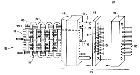
Figure 8 illustrates part of an active
interconnect assembly 130 designed according to one
embodiment of the present invention. Interconnect i~0
includes woven structure 132 and connector 134. ~s
CA 02141525 2001-O1-29
78626-1
16
described above, both optical fibers 136 and electrical
conductors 138 are positioned in channels formed by supporting
fibers 140, the structu~-a being completed by woof strands 142.
Connector 134 comprises three sections 144, 146, and 148.
Optical fibers 136 feed through section 144 while conductors
138 are coupled to elect:r_ical contacts 150. Section 146 mates
with section 144 with the help of guide pins 152, section 146
having an array of opto~electronic translation devices 154 and
electrical feed-through~~ 156. Section 146 mates with section
148, also with the help of guide pins 152. Pins 158 on section
146 connect with pins 1E;0 on section 148. If connector
sections 146 and 148 area omitted, section 144 is a passive
connector with optical fibers and electrical contacts. Passive
connectors may also corm>rise only optical fibers, i.e., no
electrical contacts. If only one section contains electrical
contacts, the active part: of the interconnect is single-ended.
Figures 9A-9C depict a connector 100 to which an
optical fiber ribbon 102 constructed according to the present
invention is coupled. Connector 100 has 52 optical
interconnects in the space of 3.81 cm (the length of ceramic
plate 104). Ceramic plate 104 has 52 holes which are used to
establish the position of the optical interconnects. This
translates to nearly 35 optical interconnects per inch. The
addition of electrical conductors in the interconnect assembly
necessitates an increase in the length of connector 100 which
is dependent upon the size of the conductors, and is typically
around 12 mils per conductor.
The active interconnect capability made possible by
the incorporation of electrical conductors into the optical
interconnect of the present invention results in several
advantages. First, by placing signal translation elements in
the interconnect hardware, the complexity of the board
CA 02141525 2001-O1-29
78626-1
16a
assemblies connected by the interconnect hardware is
correspondingly reduced. Second, by removing the opto-
electronic translation modules from system board assemblies,
more control over system power dissipation may be exercised.
This is because the heat transfer characteristics of the
interconnect assembly which now houses the translation
17
modules is more readily controllable than the board'
environment of previous systems. For example, a packaging
material having appropriate thermal characteristics and a
package shape may be chosen for the interconnect assembly to
tailor the heat transfer characteristics of the assembly to
fit the power dissipation requirements of the intended
application.
' Third, system partitioning is simplified because
the interface at the board level may now be either entirely
optical or entirely electronic. Finally, the multiplexing
and demultiplexing of optical signals through a limited
number of high speed fibers which was required in previous
interconnects becomes unnecessary because of the point to
point transmission made possible by the high optical fiber
density of the present invention. As a result, systems
incorporating the present invention may operate at speeds
limited only by the optical fibers themselves and the number
of optical fibers in use. It will be understood that the
types of opto-electronic arrays in use at either end of the
optical fibers also impact speed.
The flexibility of the woven structure of the
present invention reduces the need for optical switching
devices and such optical elements as mirrors and prisms,
thereby further simplifying opto-electronic systems. The
structure's flexibility also facilitates interconnect
capability in a direction out of the plane formed by the
woven structure. Figure 9C illustrates how, for example, an
optical backplane 106 may be coupled to connector 100 via
ribbon 102 for such a connection. An opto-electronic
module, for example, may be inserted at this connection
point. Figure 9C is a side view of connector 100 mated urith
a connector 101. With the application of an appropriate
bend technique to the woven structure of the invention, a
new type of optical backplane connection is thus made
~5 possible. one type of bend technique which lay be employed
to control the bend radius of the optical fibers involves
~he use of an elastomer coating, the thickness of trthich tt~a~r
be varied over the structure to provide the desired degree
;2141~~~
18
of control for particular segments of the structure. This
technique may be used independently, or in combination with
other bend control techniques such as those discussed below.
Figures l0A and lOB depict a connector 110 in
which a connection out of the plane of backplane 112 formed
according to the invention may be_ achieved without the
danger of optical discontinuities in the optical fibers 114.
Internal control of the optical fiber bend radius is
accomplished by means of a chamfer structure 116 inside
connector assembly 110. A top view of ceramic plate 118 is
also shown. The elastomer coating described above may be
employed in addition to the chamfer structure to provide an
additional degree of control of the fiber bend radius.
Figures 11A and 11B also depict a connector 120 in
which a connection out of the plane of backplane 122 formed
according to the invention may be achieved. Internal
control of the optical fiber bend radius is accomplished by
means of a rod 124 inserted during manufacture of optical
backplane 122. The diameter of rod 124 is such that the
actual bend radius of optical fibers 126 will be greater
than or equal to the rated bend radius as specified by the
manufacturer of the optical fibers, i.e., the bend radius
below which scattering of light and/or unreliable operation
of the optical fibers occurs. ~ top view of ceramic plate
128 is also shown. The elastomer coating described above
may be employed in addition to the rod structure to provide
an additional degree of control of the fiber bend radius.
In addition to its use in linear arrays and
interconnects, the woven fiber optic structure provided by
the present invention may be employed in two-dimensional
interconnects, also known as X-Y arrays. Figures 12A-12C
are different views of one embodiment of an X-Y array
interconnect 180 designed according to this aspect of the
present invention. In one embodiment, the woven structure
;5 of the invention is cut into strips 182 having a desired
width 184 determining the dimension of the array (and thus
the number of optical channels) in the X-direction. ~tri,~=_
182 are then layered in the Y-direction having plates 136
=~141~2~
19
therebetween to control the spacing in the Y-direction. In
a specific embodiment, plates 186 have sections 187 machined
therein to accommodate woven strips 182. Plates 186 may
comprise such materials as ceramic, silicon', plastic, or
metal. Plates 186 provide the structure to which a
faceplate 188 may be attached which holds the optical fibers
190 in defined positions for transmission, switching, or
routing of information. If rigidity is desired, plates 186
may be extended between strips 182 for any length along
interconnect assembly 180. Alternatively, the entire
assembly 180 may be placed in a hard epoxy.
Active interconnects, such as those described
above with reference to Figure 8, as well as passive
interconnects, may be layered in the manner described. In
specific embodiments, faceplate 188 may hold active devices.
Metal may be used for plates 186 in the case of active
interconnects in order that plates 186 may serve as heat
dissipation elements. If an active interconnect is large,
the ability to control spacing for heat dissipation becomes
increasingly important. Silicon substrates or ceramic
plates may be used for wire routing. For passive
interconnects, plastic spacing material is usually
sufficient.
Many strips 182 may be layered, allowing for a
c5 large number of channels in a relatively small space. In a
more specific embodiment, each of strips 182 may be coated
with an elastomer or other material (e. g., rubber epoxy)
providing both stress relief and protection to the optical
fibers 190 as discussed above with regard to elastomer
~0 coating of one-dimensional interconnects. The thickness of
such an elastomer coating may further be varied to provide
the spacing between strips in place of, or in addition to
plates 186 described above. Each strip 182 may be sheathed.
The entire assembly 180 may also be sheathed with the
~5 optical fibers 190 extending therefrom.
In another embodiment, instead of emplovina
separate strips 1s2 of moven structure as describe~t above,
an X-Y array interconnect may be constructed by repeatedly
w1~1~~~
folding the woven structure of the invention back on itself
in an accordion-like fashion. The folds are made along the
warp direction of the structure. In such an embodiment, the
number of woof strands holding the structure together
5 between the strips is kept to a minimum, i.e., approximately
2 to 4 strands per inch. This enables the woof strands to
hold the structure together without inhibiting the folding
of the structure as described, thus enabling ease of
assembly. Spacing between layers may be provided as
10 described above.
In a specific embodiment, faceplate 188 may have
microlenses 192 attached to optical fibers 190 on the
surface of faceplate 188. Index matching fluid, and/or
anti-reflective coating may be applied to microlenses 192
15 and/or optical fibers 190. Microlenses 192 would serve to
alleviate alignment problems where a large number of
channels in a small space are desirable, such as imaging,
large-scale switching, optical information management for
large systems, and other such applications. Alternatively,
20 faceplate 188 could contain ball lenses. Facilitating
alignment through the use of lenses may be done with the
one-dimensional linear array interconnects as well as with
the two-dimensional X-Y array interconnects.
While the invention has been particularly shown
and described with reference to specific embodiments
thereof, it will be understood by those skilled in the art
that the foregoing and other changes in the form and details
may be.made therein without departing from the spirit or
scope of the invention. The scope of the invention,
therefore, should be limited only by the following claims.