Note: Descriptions are shown in the official language in which they were submitted.
~~'~'
1.
INTERFERENCE AVOIDANCE SYSTEM FOR VEHICOLAR RADAR SYSTEM
BACKGROUND OF THE INVENTION
1. Field of the Invention
This invention relates to vehicular target detection
systems, and more particularly, to a method and
apparatus for interference avoidance by changing the
transmit frequency of a vehicular target detection
system when interference is encountered.
2. Description of Related Art
There is a continuing need to increase the density of
vehicles traveling the world's roadways, and
simultaneously to improve the safety of highway vehicle
operations by preventing highway vehicles from ,
colliding with moving and stationary objects (such as
roadside obstacles and other vehicles). One means for
accomplishing these seemingly contradictory goals is to
monitor environmental conditions, such as the relative
speed, direction of travel, and distance between
vehicles sharing the roadway, and to use such
information to provide direct indications to the
vehicle's operator of potential danger. It is becoming
increasingly more common for vehicular engineers to
consider the use of target detection systems, such as
microwave radar systems, as the means to monitor such
environmental conditions.
35
A number of vehicular target detection systems are
currently known in the art. One such system includes
a radar system which transmits three time-multiplexed
signals, two of which
~A
2. ~'~
are used to determine the range of an object (target),
and the third of which is used to determine the
relative speed of the target. The upper and lower
frequencies are separated from the center frequency by
about 250 kHz with the center frequency being about
24.125 GHz. The system transmits the signals, and
receives reflections from targets. By processing the
reflected signal, the system determines the range and
relative speed of the targets.
In another vehicular target detection system described
in copending Canadian Patent Application, Serial No.
2,141,546 ( entitled "Multi-Frequency Multi-Target
Vehicular Radar System Using Digital Signal
Processing," assigned to the assignee of the present
invention, the microwave transceiver generates and
transmits a signal in which only two frequencies are
time division multiplexed. The two frequency radar
' system uses a digital signal processor within the
digital electronics section to determine the range and
relative motion of targets based upon the difference
between the frequency of the transmitted signal and the
frequency of reflections of the transmitted signal
subsequently received by the transceiver. The digital
signal processor performs a series of Fast Fourier
Transforms (FFT) on a digitized representation of the
output of a radio frequency (RF) mixer. The analog
output of the mixer is a signal having a frequency
equal to the difference between the frequency of the
transmitted signal as applied to one input of the RF
mixer, and the summation of reflections of the
transmitted signal after reflecting off targets in the
environment, as well as various other signals which
have been received by the transceiver, as applied to a
second input to the RF mixer. Analyzing the results of
the FFT allows a microprocessor within the digital
electronics section to determine the range and relative
~' t =~
F~ J,: ~:~y,,
ee-
WO 94/04939 ~ ~ ~ ~ ~ ~ ~ PCT/US93/07506
3.
motion of a multiplicity of targets. The micro-
controller generates visual and audible warnings to the
vehicle operator.
However, a significant problem which plagues both of
these target detection systems (and in fact all target
detection systems which rely upon receiving a
reflection of a transmitted signal from a target) is
interference with the transmitted signal and the
reflections thereof, which may make detection of such
reflections difficult or impossible. For example,
microwave interference caused by a variety of sources
of microwave energy, such as other vehicular radar
systems, burglar alarms, automatic door openers, and
speed-measuring radar systems can render a microwave
vehicular target detection system inoperative for
periods of time which can range from fractions of a
second to minutes. Such an occurrence reduces the
effectiveness of the vehicular target system in
detecting moving or stationary objects, such as other
vehicles and roadside obstacles.
Therefore, it is desirable to provide a vehicular
target detection system that can cope with the presence
of interference in the environment in which the target
detection system is operating. The present invention
provides a solution to this problem.
WO 94/04939 ~ ~ . ' PGT/US93/07506
~14154~~
SUMMARY OF THE INVENTION
The present invention is an interference avoidance
system used in conjunction with a vehicular target
detection system. The interference avoidance system
includes a microcontroller which, in the preferred
embodiment of the present invention also controls
operations within the target detection system.
A microwave transceiver section of the vehicular target
detection system, in which the illustrated embodiment
of the present invention is incorporated, transmits and
receives microwave signals. The transmit signal is
time-multiplexed, alternating between at least two
carrier frequencies, preferably spaced about 250 kHz
apart. An oscillator, such as a Gunn diode, in the
microwave transceiver section generates the transmit
signal. A modulation signal from an oscillator
modulation circuit causes the Gunn diode to alternate
between the time-multiplexed frequencies. The time-
multiplexed transmit signal is transmitted by means of
a radar antenna. The transmit signal strikes objects
(targets) in the environment and a portion of the
transmit signal is reflected back to the antenna.
The received signal is coupled to one input of a
difference detector, such as a radio frequency (RF)
mixer used in the illustrated embodiment. A portion of
the transmit signal is coupled to a second input of the
RF mixer. The mixer outputs a difference signal having
a frequency equal to the difference between the
frequency of the transmit and the received signal. The
difference signal is coupled to the front end
electronics section, which digitizes the difference
signal. A digital signal processing section maps the
signal from the time domain into the frequency domain
by performing a mapping function, such as a Fast
WO 94/04939 "" PCT/US93/07506
~~4154~
5.
Fourier Transforms (FFT), on the digitized difference
signal.
Upon performing the FFT on the digitized difference
signal, the energy at discrete frequencies within a
selected frequency band is determined. A
microcontroller receives the results of the FFT
operation. The microcontroller analyzes the energy
spectrum to determine whether there is microwave
interference present. If such microwave interference
is present on one, or both, of the transit frequencies,
the microcontroller causes the oscillator modulation
circuit to change transmit frequencies. If
interference is again encountered, the microcontroller
again causes a change in frequency. This process is
repeated until a pair of frequencies is found which is
relatively free of the interference. In the preferred
embodiment of the present invention, the
microcontroller can choose between four pairs of
frequencies spaced about 5 MHz apart. The
microcontroller cycles through the four available pairs
of frequencies searching for a pair of frequencies that
is relatively clear of interference. In the preferred
embodiment of the present invention, if each pair of
frequencies has substantial interference, the pair of
frequencies having the least interference is
transmitted.
The details of the preferred embodiment of the present
invention are set forth in the accompanying drawings
and the description below. Once the details of the
invention are known, numerous additional innovations
and changes will become obvious to one skilled in the
art.
PGT/US93/07506
WO 94/04939
6.
BRIEF DESCRIPTION OF THE DRApINGB
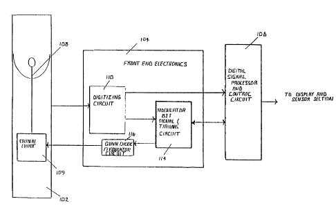
FIGURE 1 is a simplified block diagram of a two
frequency vehicular target detection system
incorporating the present invention.
FIGURE 2 is a block diagram of the digital signal
processor and control circuit of a two frequency
vehicular target detection system incorporating the
present invention.
FIGURE 3 is a detailed schematic of the oscillator
modulation circuit of the present invention.
FIGURE 4 is a table showing the logic states of each of
the control lines to the oscillator modulation circuit
of FIGURE 3, and the resulting frequencies generated by
the Gunn diode.
FIGURE 5 is a logical flowchart showing the procedure
followed by the present invention when interference is
encountered.
FIGURE 6 is a flowchart of the steps taken to determine
whether microwave interference is present.
Like reference numbers and designations in the various
drawings refer to like elements.
w
F
~ ~ .
DETAILED DESCRIPTION OF THE.INVENTION
Throughout this description, the preferred embodiment
and examples shown should be considered as exemplars,
rather than as limitations on the present invention.
In particular, the following description is given in
the context of a particular vehicular radar system, yet
it should be understood that the present invention may
be incorporated in any target detection system in which
the received signal, or some derivative signal, is
mapped from the time domain into the frequency domain
for the purpose of determining characteristics of
targets in the environment, such as the presence,
relative speed, and/or nature of such targets.
OVERVIEW
FIGURE 1 is a block diagram of a prior art vehicular
target detection system incorporating the present
invention. The vehicular target detection system of
FIGURE 1 includes a microwave transceiver section 102,
a front end electronics section 104, and a digital
signal processing and control section (DSPCS) 106. A
complete description of the vehicular target detection
system shown in FIGURE 1 is given in copending Canadian
Patent Application, Serial No. 2,141,546, entitled
"Multi-Frequency, Multi-Target Automotive Radar System
using Digital Signal Processing", which has been
assigned to the assignee of the present invention.
The microwave transceiver section 102 includes a radar
antenna 108 which transmits a radio frequency (RF)
signal generated by an oscillator, such as a Gunn diode
109, and receives the reflection of that signal off
objects (targets) in the environment of the vehicle
upon which the radar system is mounted. The Gunn diode
109 is controlled by an oscillator modulation circuit
-..yr.~ ~,
WO 94/04939 PGT/US93/07506
~141~4~
116 which in turn is controlled by a timing generator
circuit 114. The output from the microwave transceiver
section 102 is coupled to the front end electronics
section 104.
The front end electronics section 104 includes a
digitizing circuit 110 which receives the output from
the microwave transceiver section 102. The signal is
digitized and coupled to the DSPCS 106 which maps the
digitized signal data from the time domain into the
frequency domain, as described in the copending "Multi-
Frequency, Multi-Target Automotive Radar System using
Digital Signal Processing" patent application.
Once the signal is mapped into the frequency domain,
microwave interference is identified in accordance with
the present invention. If interference is present, a
command from the DSPCS 106 is generated to instruct the
front end electronics section 104 to change the
transmit frequency.
DETAILS OF OPERATION
The details of the operation of the preferred microwave
transceiver section 102 and digitizing circuit 110 are
fully disclosed in the copending "Multi-Frequency,
Multi-Target Automotive Radar System using Digital
Signal Processing" patent application. However, it
should be understood that the details of such sections
of the radar system are not necessary for enabling a
person skilled in the art to make and use the present
invention, and do not hinder this description from
setting forth the best mode contemplated by the
inventors of carrying out the present invention.
The DSPCS 106 is shown in greater detail in FIGURE 2.
The DSPCS 106 includes a field programmable gate array
(FPGA) 202, digital signal processor (DSP) 204, a
WO 94/04939 PCT/US93/07506
21~154~
9.
microcontroller 206, and a data storage device, such as
a high speed RAM 208 used in the illustrated
embodiment. The FPGA 202 receives the digitized signal
data output by the digitizing section 110. The FPGA
202 loads the digitized signal data into the RAM 208 in
known fashion and generates a direct memory access
(DMA) request to the DSP 204 to pass control of the bus
210 to the FPGA 202 when each full word of data has
been stored.
When sufficient data has been stored in the RAM 208,
the DSP 204 calculates the FFT on the digitized signal
data so stored. The DSP 204 is coupled to the
microcontroller 206. In the two frequency radar system
of the copending "Multi-Frequency, Multi-Target
Automotive Radar System using Digital Signal Process-
ing" patent application, the results of the FFT include
the power level of the low frequency noise floor and
the high frequency noise floor. The power level of the
low frequency noise floor is the average power at each
frequency below f/2, and the power level of the high
frequency noise floor is the average power at each
frequency above f/2, where f is the bandwidth of
interest. The bandwidth of interest in the illustrated
embodiment of the present invention are those
frequencies that are approximately within the frequency
range of 0 to 7.5 kHz. The results of theTFFT are
coupled from the DSP 204 to the microcontroller 206,.
The microcontroller 206 analyzes the results of the FFT
and determines whether microwave interference is
present.
In the preferred embodiment of the present invention,
to determine if microwave interference is present the
microcontroller 206 compares the amount of power in the
noise floor with a predetermined threshold set in the
microcontroller 206. In an alternative embodiment of
WO 94/04939 ' ~ PCT/US93/07506
214154~~:
10.
the present invention, the microcontroller 206
dynamically determines the threshold. In one such
alternative embodiment, the threshold is determined by
averaging the power level in the noise floor across a
band of frequencies sampled at specified intervals in
frequency and time. The threshold is set at a
predetermined fixed level above the average level of
the noise floor over a specified period of time.
In another embodiment, the noise floor is determined by
direct input from an operator based upon knowledge of
the local environment. In yet another embodiment, an
offset from a fixed threshold is used to determine the
maximum power allowable in the noise floor. For
example, if the threshold were set at a power level of
"X" dBm, the microcontroller 206 would determine that
interference exists whenever the noise floor had a
power level "Y" d8 above "X" dBm. The offset "Y" is
programmable or is determined based upon the level of
the noise floor. Either a look-up table or a formula
is used to determine the offset in those embodiments in
which the offset is determined based upon the level of
the noise floor.
The FPGA 202 acts as an interface between the
microcontroller 206 and the front end electronics
section 104. Commands from the microcontroller 206 are
sent to the FPGA 202 in a synchronous serial format
containing a header and an end byte, in known fashion.
The commands preferably contains 8 serial bits. In the
preferred embodiment, two of the bits of the command
are used to indicate which of 4 different base
frequencies the Gunn diode 109 is to transmit
(frequency A, B, C, or D). The remaining bits of the
command are not relevant to the present invention.
WO 94/04939 2 Z 41 ~ 4 ~ PL'f/L1S93/07506
11.
If the microcontroller 206 determines that there is
sufficient microwave interference to warrant changing
the transmit frequency, the microcontroller 206 sends a
"change frequency" command to the FPGA 202. The FPGA
202 then sends the command in synchronous serial format
to the front end electronics section 104 where it is
received by the timing generator circuit 114. The
timing generator circuit 114 decodes the command and
sets or resets control lines coupled to the oscillator
modulation circuit 116.
The preferred embodiment of the present invention is
incorporated in a radar system in which the transmit
frequency alternates between two channels to permit the
radar system to determine the range and relative speed
of targets which reflect the transmitted signal. Each
channel is assigned a frequency which may be changed
under the control of the oscillator modulation circuit
116. In the preferred embodiment of the present
invention, the difference between the frequency
assigned to channel 1 and the frequency assigned to
channel two remains approximately constant (i.e.,
approximately 250 kHz apart). The output of the Gunn
diode 109 is proportional to the voltage applied to a
frequency control input 118 on the Gunn diode 109.
Therefore, by controlling the voltage level applied to
the frequency control input 118, the oscillator
modulation circuit 116 determines the transmit
frequencies associated with each channel.
FIGURE 3 is a detailed schematic of the oscillator
modulation circuit 116. The oscillator modulation
circuit 116 has 6 control lines FC1, FC2, FREQ A, FREQ
B, FREQ C and FREQ D. Control lines FC1 and FC2
determine the base frequency which the Gunn diode 109
generates. Control lines FC1 and FC2 are only changed
when a command is issued by the microcontroller 206.
PCT/US93/07506
WO 94/04939
12.
Each of the control lines FC1 and FC2 are coupled to a
resistor divider network R1, R2 which sets the voltage
at the base of respective transistors Q1 and Q2. When
the two control lines FC1, FC2 are set to a logical
"1", the voltage at the base of each associated
transistor Q1, Q2 rises, causing the transistor to
conduct. When either transistor conducts, the
resistance between a voltage regulator adjust input ADJ
and ground is reduced. Reducing the resistance between
the voltage regulator adjust input ADJ and ground
reduces the level of the voltage at a voltage regulator
output VOUT. In the preferred embodiment of the
present invention, the voltage regulator U1 is a
standard component, such as part No. LM317 manufactured
by National Semiconductor.
The regulated output voltage at the VOUT port of the
'voltage regulator U1 changes when one or both
transistors Q1, Q2 are conducting. Each of the four
(22) possible combinations of states of the control
lines FC1, FC2 cause a different voltage to be output
by i~he voltage regulator U1. The table in FIGURE 4
illustrates the relationship between the FC1, FC2
control line states and the transmit frequency in the
preferred embodiment.
It should be understood by those skilled in the art
that the frequency generated by a Gunn diode 109 is, in
general, not linearly proportional to the control
voltage applied to the Gunn diode 109. Therefore, the
difference in control voltage required to produce a
difference in frequency at any one particular frequency
is different from the difference in control voltage
required to produce an equal difference in frequency at
a second frequency.
21 ~ I ~ 4 8 P~/LJS93/07506
WO 94/04939 C
13.
For example, in the preferred embodiment, if a control
voltage of one volt is applied to the frequency control
input 118 of a particular Gunn diode 109, the Gunn
diode generates an output frequency of 24.125- GHz. By
reducing the voltage by 0.8 volts, the frequency
decreases to 24.124750 GHz. Therefore, a voltage
difference of 0.8 volts alters the frequency by 250
kHz. When a voltage of 3 volts is applied to the
frequency control input 118 of the same Gunn diode 109,
the Gunn diode generates an output frequency of 24.110
GHz. In order to raise the frequency to 24.110250 GHz,
the control voltage must be increased 3.4 volts (a
difference of 0.4 volts).
It can be seen from this example that, in order to
cause the Gunn diode 109 to alternate between two
channels spaced approximately 250 kHz apart, the
control voltage must alternate between two voltage
levels which differ by an amount that is dependent upon
the frequencies of the two channels. In the preferred
embodiment of the present invention, each switching
transistor Q3-Q6 and associated adjustable resistive
network R4-R7 generates the two distinct voltages
associated with a pair of transmit frequencies spaced
about 250 kHz apart.
The remaining four control lines FREQ A, FREQ B, FREQ
C, and FREQ D are "clock" lines which alternate between
a logical "1" state and a logical "0" state at a
frequency which is predetermined by timing
considerations within the radar system. Only one of
these four clock lines FREQ A, FREQ B, FREQ C, FREQ D
is active at a time. The remaining three are held at a
logic "0" state. When each of the clocks FREQ A, FREQ
B, FREQ C, FREQ D are at a logical "0" state, the
voltage applied to the frequency control input 118 is
substantially equal to the voltage at the output VOUT
WO 94/04939 ~ 141 ~ 4 8 P~/US93/07506
14.
of the voltage regulator U1. This is because the
conductive paths through the Gunn diode 109 and the
transistors Q3-Q6 have a high impedance, and thus
conduct little current, resulting in a minimal voltage
drop across the resistor R3.
When any one of the transistors Q3-Q6 conduct, current
is drawn through the resistor R3 causing the voltage
drop across the resistor R3 to increase. Thus, the
voltage supplied to the frequency control input 118 is
reduced from the level present when none of the
transistors Q3-Q6 are conducting. A resistive network
R4-R7 is associated with each transistor Q3-Q6. Each
resistive network R4-R7 includes a fixed resistor R4a-
R7a and a variable resistor R4b-R7b. Adjusting any
variable resistor R4a-R7a changes the voltage at the
frequency control input 118 when the transistor Q3-Q6
associated with the variable resistor R4a-R7a is
conducting. Therefore, the ratio of the voltage at the
frequency control input 118 when the transistor Q3-Q6
is conducting (i.e., when channel 1 is active) with
respect to the voltage at the frequency control input
118 when the transistor Q3-Q6 not conducting (i.e.,
when channel 2 is active) can be adjusted. In this
way, the difference between the frequency transmitted
when each clock FREQ A, FREQ B, FREQ C, FREQ D is low
and the frequency transmitted when the same clock is
high can be adjusted. The frequencies that are
transmitted in the preferred embodiment of the present
invention are listed in table 1 of FIGURE 4. It should
be clear to those skilled in the art that the
oscillator modulation circuit 116 may be implemented
with a monolithic integrated digital to analog (D/A)
converter circuit, such that digital inputs to the D/A
converter circuit cause the output voltage of the
oscillator modulation circuit 116 to change to a known
value which results in a known frequency. Thus by
21414
WO 94/04939 PCT/US93/07506
t_
15.
controlling the digital inputs to such a monolithic
integrated D/A converter circuit, the oscillator may be
controlled to generate the desired frequencies.
Applying the above discussion to an example will
further illuminate the inventive aspects of the present
invention. In this example, assume that a radar system
is initially operating under normal conditions at a
transmit frequency that alternates between 24.125 GHz
and 24.125250 GHz at regular intervals (i.e., the clock
control line FREQ A is actively alternating between
high and low logic levels).
The transmit signal is emitted into the environment by
means of the antenna 108. Part of the signal is
reflected back to the antenna 108 by targets which the
transmit signal strikes. The received reflections of
the transmit signal are contrasted with the transmit
signal, demultiplexed, and digitized. The digitized
samples are sent as a synchronous serial data stream of
24 bit words from the digitizing circuit 110 to the
FPGA'~202. The FPGA 202 writes each 24 bit word
directly to the RAM 208. Each time a digitized sample
of the signal is stored in the RAM 208, the DSP 204 is
interrupted by the FPGA 202. During normal operations,
the DSP 204 performs an FFT on the most recently stored
4,096 digitized samples of each channel. Thus far in
this example, each of the above described functions is
described in the copending "Multi-Frequency, Multi-
Target Automotive Radar System using Digital Signal
Processing" patent application.
When the preferred embodiment of the present invention
is incorporated in a target detection system, such as
the two frequency radar system of the example above,
the microcontroller 206 within the target detection
system takes on additional duties. However, an
WO 94/04939 PCT/US93/07506
z~4m~s
16. .
alternative embodiment of the present invention has an
independent microcontroller which performs all the
necessary control functions without burdening the
target detection system microcontroller 206. FIGURE 5
is a flow chart of the operation of the present
invention as incorporated within such a two frequency
digital radar system. Each step of the flow-chart can
be performed in any order unless otherwise specified.
The microcontroller 206 receives data from the DSP 204
which indicates the power level of the noise floor in
the current environment. The microcontroller 206
determines whether there is microwave interference
based on this information (STEP 400).
If the noise floor is below the threshold set within
the microcontroller 206, the microcontroller 206
continues to monitor the output of the DSP 204 to
ensure that the noise floor remains below the
predetermined threshold. If, however, the noise floor
rises above the predetermined threshold, the
microcontroller 206 sends a "change to frequency n"
command to the oscillator modulation circuit 116, as
disclosed above, to change the transmit frequency (STEP
401). The microcontroller 206 also sends a command to
the FPGA 202 to flush all the samples stored thus far,
since such samples have been contaminated by the
interference (STEP 402).
After flushing the samples from the RAM 208, new data
must be collected. Once the digitized samples are
flushed, the system is "blind" until new samples can be
collected and an FFT performed. Therefore, in order to
expedite the process of determining the status of the
environment, the DSP 204 begins counting the number of
new samples stored in the RAM 208. Each time the FPGA
202 receives a new digitized sample, it initiates a DMA
request. A DMA request causes the DSP 204 to release
WO 94/04939 ' - , PGT/US93/07506
17.
the bus shared by DSP 204, the FPGA 202, and the RAM
208. Once the DSP 204 has released the bus, the FPGA
202 writes the digitized sample to the RAM 208. In the
preferred embodiment, the samples are organized as
blocks of samples within the RAM 208. A block
comprises two memory areas, each having 512 samples.
The DSP 204 is interrupted when an entire block of
samples have been stored in the RAM 208. Therefore, by
counting either the number of interrupts generated by
the FPGA 202, or by counting the number of bus accesses
made by the FPGA 202, the DSP 204 can determine the
number of samples of digitized signal data stored in
the RAM 208.
After flushing the old samples, the DSP 204 monitors
the FPGA 202 to determine when there are 1,024 new
digitized samples associated with each channel in the
RAM 208 (i.e., when at least 2 interrupts have
occurred) (STEP 403). When at least 1,024 new
digitized samples associated with each channel have
been stored in the RAM 208, the DSP 204 performs an FFT
on the last 1,024 such samples. The microcontroller
206 receives the results of the FFT and determines
whether there is any microwave interference (i.e., in
the preferred embodiment of the present invention,
whether the noise floor is above the predetermined
threshold) (STEP 405). If there is microwave interfer-
ence, the system repeats STEPS 401-405 until a pair of
frequencies are transmitted that is relatively free of
interference. In the preferred embodiment of the
present invention, there are only four possible pairs
of frequencies. The microcontroller 206 selects the
first pair of frequencies that appear to be relatively
free of interference. If all frequencies have a
relatively large amount of interference, the
microcontroller selects the frequency pair with the
least interference.
WO 94/04939 ~ ~ 41 ~ ~ g PCT/US93/07506
18.
It should be obvious to those skilled in the art that
the number of frequencies to which the transmitter can
switch is a function of the Gunn diode range and the
number of control lines and associated circuits
included in the oscillator modulation circuit 116.
Therefore, by adding additional control lines and
associated control circuits, additional transmit
frequencies may be added. It should also be obvious to
those skilled in the art that, for each added
transistor circuit such as those transistor circuits
associated with transistors Q1 and Q2, the number of
frequencies increases by a power of 2. However, for
each new frequency added, a circuit such as the circuit
associated with each transistor Q3-Q6 also must be
added to the oscillator modulation circuit 116.
If the FFT is performed on the last 1,024 digitized
samples associated with each channel of the signal
(STEP 404) and the microcontroller 206 determines that
the power level of the noise floor is below the
threshold (STEP 405), the DSP 204 monitors the FPGA 202
to determine when 2,048 digitized samples associated
with each channel have been stored in the RAM 208. The
DSP 204 continues to perform an FFT on the last 1,024
digitized samples associated with each channel (STEPS
404-406) until at least 2,048 digitized samples
associated with each channel have been stored in the
RAM 208 (STEP 406). When at least 2,048 digitized
samples associated with each channel have been stored
in the RAM 208, the DSP 204 performs an FFT on the last
2,048 digitized samples associated with each channel
(STEP 407).
After performing an FFT on the last 2,048 digitized
samples associated with each channel, the
microcontroller 206 again determines whether the power
in the noise floor is below the threshold, indicating
WO 94/04939
214 ~ ~ 4 $ ~ , . .. PCT/US93/07506
19.
that no microwave interference is present (STEP 408).
If interference is detected, the system returns to STEP
401 and progresses through the subsequent steps again.
If no interference is present, the DSP 204 determines
whether 4,096 digitized samples associated with each
channel have been stored (STEP 409) in the RAM 208.
The DSP 204 continues to perform an FFT on the last
2,048 digitized samples associated with each channel
that have been stored until the FPGA 202 has stored in
the RAM 208 at least 4,096 digitized samples associated
with each channel (i.e., until 8 interrupts have been
made by the FPGA 202).
When at least 4,096 digitized samples associated with
each channel have been stored the DSP 204 performs an
FFT on the 4,096 samples associated with each channel
which were last stored (STEP 410). Once again the
microcontroller 206 determines whether there is
interference present (STEP 411). If there is no
interference present, the DSP 204 continues to perform
an FFT on the last 4,096 samples associated with each
channel as each new sample is stored in the RAM 208.
If interference is encountered, the system repeats the
process from STEP 401.
By flushing the data that was previously stored in the
RAM 208, contamination that is introduced by the
interference, and which could cause target errors, is
erased. By re-calculating the FFT on an initial 1,024
samples of each channel, the amount of time required to
regain the targets and continue tracking is reduced by
75% of the time that would be required if 4,096 samples
associated with each channel were necessary before
performing the next FFT.
FIGURE 6 is a flowchart of the steps taken to determine
whether microwave interference is present. An RF
WO 94/04939 PCT/US93/07506
2141 ~g
20.
signal is transmitted (STEP 501) and the reflections
thereof, together with signals generated by sources
external to the present invention, are received (STEP
502). The received signals are compared with the
transmitted signal and a difference signal having a
frequency equal to the difference between the frequency
of the received and transmitted signals is generated
(503). The difference signal is digitized (STEP 504)
and each of the resulting digital samples of the
difference signal are stored in the RAM 208 (STEP 505).
The samples are read from the RAM 208 by the DSP 204
which performs an FFT operation on the samples. The
samples are thus mapped from the time domain into the
frequency domain (STEP 506). The FFT operation results
in a series of power levels corresponding to a series
of frequencies. The power level of selected frequency
bands are compared to a threshold which may be
determined in a number of ways (STEP 507). If the
power in the selected frequency band is greater than
the threshold value, interference is assumed to be
present (STEP 509). If the power in the selected
frequency band is not greater than the threshold value,
interference is assumed not to be present (STEP 508).
It should be understood that the present invention
allows a vehicular target detection system to remain
effective in a normally hostile environment in which
interference would otherwise reduce the effectiveness
of the target detection system. By detecting the
presence of interference and commanding a change of
frequency, the present invention provides a dynamic
interference avoidance system that can respond to the
changing interference patterns encountered when moving
through differing environments, such as urban and
suburban environments. Furthermore, the present
invention provides fast recovery from contamination of
the digital data stored due to interference, by
WO 94/04939 ~ PCT/US93/07506
21.
reducing the number of bytes of digitized signal data
required to determine the presence, range, and relative
speed of a target.
A number of embodiments of the present invention have
been described. Nevertheless, it will be understood
that various modifications may be made without
departing from the spirit and scope of the invention.
For example, the noise floor threshold against which
the microcontroller 206 compares the measured noise
floor power level may be set in any number of ways,
such as being programmed into the system by an
operator, dynamically determined, fixed, or fixed with
a programmable or dynamically determined offset.
Furthermore, the microcontroller 206 can tune the
oscillator 109 to any number of frequencies, and is not
limited by the number of frequencies of the above
disclosed embodiment. Still further, any digital to
analog converter circuit may be used to control the
voltage to the frequency control input 118 to the
oscillator 109. It should also be understood that the
present invention may be used with any form of surface
transportation, such as automotive vehicles, trains,
trolleys, and boats. Most importantly, it should be
clear that the invention is independent of the
particular target detection system into which the
invention is incorporated and the invention, as herein
described, could be incorporated into any target
detection system in which a reflection of a transmitted
signal is relied upon to detect the target and in which
it can be determined that interference with the
transmitted or reflected signal is present.
Accordingly, it is to be understood that the invention
is not to be limited by the specific illustrated
embodiment, but only by the scope of the appended
claims.