Note: Descriptions are shown in the official language in which they were submitted.
'l -
DUAL SENSITIVITY STUD SENSOR ~ 5 5 3
BACKGROUND OF THE INVENTION
Field of the Invention
This invention relates to an electronic sensor, and,
in particular, to a sensor suitable for detecting the location
of studs behind a variety of surfaces, including walls, floors
and similar type structures. More specifically, the invention
relates to an electronic stud sensor with two sensitivity
modes for determining the location of studs behind either
thick or thin surfaces, and with the ability to inform the
user when the sensor has been calibrated over a stud.
Description of the Prior Art
U.S. Pat. No. 4,464,622 issued August 7, 1984, and
discloses an electronic wall stud sensor particularly suitable
for locating a wall stud positioned behind a wall surface.
The sensor detects the stud by measuring a change in the
capacitance of the wall due to the presence of a stud while
the sensor is moved along the wall surface. The sensor
includes a plurality of capacitor plates mounted in the sensor
close to the wall surface, a circuit for detecting any changes
in the capacitance of the capacitor plates due to a change in
the dielectric constant of the wall caused by the location of
a stud positioned behind the wall surface and immediately
adjacent to the capacitor, and an indicator for indicating the
change in capacitance of the capacitor plate, thereby
indicating the wall stud position. The sensor also alerts the
operator when calibration is occurring.
While the above described electronic wall stud
sensor operates as described to locate studs in walls,
experience has shown that its performance could be improved in
-- 1 --
~ 70128-285
W094/04932 PCT/US93/07433
~14~15~3 2
several respects. The stud sensor is unable to reliably
sense studs through surfaces significantly thicker than
the typical 5/8 inch sheetrock wall. For instance, the
sensor can not sense floor joists (another type of stud)
5 under a combination of 3/4 inch subfloor and 1/4 inch oak
flooring.
Moreover, the stud sensor is incapable of informing
the operator when the sensor has been calibrated over a
stud. When the sensor is subsequently moved from the stud
10 after completion of this incorrect calibration, it is
unable to detect studs and no indication is given that the
sensor was incorrectly calibrated. Finally, the stud
sensor's correct calibration voltage has a tendency to
"leak off," due to use of a sample-and-hold capacitor.
15 This results in less accurate readings after approximately
a minute of use.
Therefore, there is a need to sense studs through -
both thick and thin surfaces. There is also a need to
determine when the device has been calibrated over a stud,
20 and informing the operator of this. Further, there is a
need for a circuit which maintains calibration
indefinitely.
SUMMARY OF THE INVENTION
In accordance with the present invention, a dual
25 sensitivity stud sensor senses studs through both thick
and thin surfaces. The sensor also has the ability to
sense both an increase and a decrease in density. This
allows the device to inform the user when the sensor has
been incorrectly calibrated over a stud. Further, the
30 device will notify the operator when the surface being
sensed is either too thick or too thin for stud detection.
By use of a digita~ register to store calibration data,
calibration is maintained indefinitely while the stud
sensor is powered on.
Finally, through use of a tri-state driver and a D
type flip-flop, a single IC pin of the stud sensor
circuitry is employed as both an input and an output, and
becomes, in effect, a bi-directional port.
The present invention may be summarized, according
to a first broad aspect, as a portable device for locating a
stud positioned behind a surface comprising: a sensor
determining additional capacitive loading caused by the stud
while said sensor moves along the surface approaching the stud
and providing digital data signals as output when said
additional capacitive loading is determined; a digital
averager for receiving the data signals from said sensor and
averaging them; and a display processor for receiving the
averaged data and in response providing an indication of the
stud position.
According to a second broad aspect, the invention
provides a portable device for locating a stud positioned
behind a surface comprising: sensor circuitry including a
differential capacitive plate circuit, for sensing unbalanced
capacitive loading of two plates in the differential
capacitive plate circuit, and providing digital data signals
when unbalanced capacitive loading of the two plates is
sensed; and a display processor receiving said digital data
signals and in response providing an indication of the stud
position, said display processor providing a linearly stepped
voltage to said differential capacitive plate circuit as an
offset voltage to put the sensor circuitry in a null state.
According to a third broad aspect, the invention
provides a method for locating a stud positioned behind a
surface comprising the steps of: sensing additional capacitive
70128-285
.-;
", ,
5 3
".,.
loading caused by the stud while a sensor moves along the
surface approaching the stud; sending digital data signals
when said additional capacitive loading is sensed; averaging
said data signals digitally over a predetermined time period;
and displaying said data signals.
BRIEF DESCRIPTION OF THE DRAWINGS
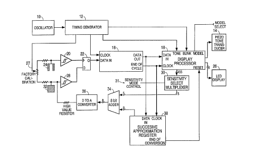
Figure 1 is a block diagram of an embodiment of the
invention.
Figure 2 shows various waveforms of the sensing
portion of the circuit of FIG. 1.
Figure 3 is a schematic of a circuit allowing both
input to and output from a single pin of an integrated
clrcult .
Figure 4 is a schematic showing the capacitive
memory for keeping track of the time at which the stud sensor
is powered up.
DETAILED DESCRIPTION OF THE INVENTION
Operation
Shown in FIG. 1 is an embodiment of the invention
for locating positions of studs behind a surface through
capacitive sensing.
As in the prior art patent referenced above,
operation of this circuit detects the change in capacitive
loading of the sensor plates 24 and 32 as they are moved along
a surface and into proximity with a stud. Plate 32 is
positioned between a pair of coupled plates 24 in the same
manner as the plates in the prior art. Schmitt triggers 20
and 28 function in the same manner as the one shot multi-
- 3/1 -
70128-285
.. "~ a ~
vibrators described in the prior art patent. Therefore, as in
the prior art patent, additional capacitive loading due to the
presence of a stud unbalances a differential capacitive plate
circuit.
However, in accordance with one feature of this
invention, the unbalance is traced via a counter in the
display processor 18 which injects an offset voltage into the
sensor plate circuit via a digital-to-analog (D/A) converter
36. Each step of the counter corresponds to a unique voltage
step certain steps of which are also
- 3/2 -
70128-285
W094/04932 PCT/US93/07433
2141~3 4 _
associated with a particular LED in the LED display 26.
As additional capacitive loading occurs due to the
stud density, the LEDs in LED display 26 correspondingly
change, signaling the stud's presence. The unit is
5 calibrated such that the top LED illuminates as the unit
is directly over the edge of a stud, with intermediate
LEDs showing the approach to the stud's edge. A tone
output from the piezo electric tone transducer 14 occurs
concurrent with the illumination of the top LED of the LED
10 display 26.
The capacitive null of the sensor plates, i.e., when
each sensor plate is equally "loaded," is also sensed
through the Schmitt triggers 20 and 28. As shown in FIG.
2, the outputs from these Schmitt triggers then drive
15 respectively the clock input 58 and data input 60 of a D
type flip-flop 22. If the plates are unequally "loaded,"
either the clock input 58 or the data input 60 to the
flip-flop 22 will occur first, setting the output 62 of
the flip-flop to either a one or a zero. A null, or
20 balanced differential plate capacitatance state, is
detected by increasing, in small incremental steps, via
the digital-to-analog (D/A) converter 36, the offset
injection voltage to the sensor plate circuit until the
output 62 of the flip-flop 22 changes state. This signals
25 a null condition.
As also shown in FIG. 2, the sensor plate circuit is
driven by an excitation signal 52. This excitation signal
is derived from a timing generator 12, which is in turn
driven by an oscillator 10. This excitation signal
30 consists of a 1/16 duty cycle pulse which charges the
capacitance of the sensor plates 24 and 32. The voltage
54 and 56 at the sensor plates 24 and 32 then rises
exponentially and at some point reac~es the upper voltage
threshold 64 of the Schmitt triggers 20 and 28. The
35 change in logic level at the Schmitt triggers 20 and 28
outputs then drives the D type flip-flop 22 clock input 58
and data input 60 to determine which signal, clock 58 or
W094/04932 PCT/US93/07433
~ 5 _ 21~1553
data 60, arrived first. A null condition is then defined
as the clock and data signals occurring at the same time.
In actuality, these two signals do not occur "exactly"
simultaneously but are very close at null, with a
5 resolution determined by the least significant bit
resolution of the D/A converter 36. The excitation signal
52 then goes to a "zero" for 15/16 of the excitation
period allowing the capacitance of the sensor plates 20
and 28 to fully discharge.
The data input terminal of the averager 16 is
connected to the D type flip-flop 22 output terminal. The
averager 16 receives a 10 KHz clock signal from the timing
generator 12. Therefore, every 100 microseconds, the
averager 16 determines if the output of the flip-flop 22
15 is a one or a zero. There are two counters within the
averager 16. One is a counter which counts to sixty-four,
and starts over again once it reaches sixty-four. The
other counter in the averager 16 is an accumulator
counter, and is only incremented if the input from the
20 flip-flop 22 is a one. If the input from the flip-flop 22
is zero, the counter is not incremented. Therefore, at
the end of sixty-four cycles, the accumulator counter in
the averager 16 will have accumulated the number of times
the output from the flip-flop 22 was one. If the
25 accumulator counter has accumulated less than 28 ones
after sixty-four cycles, the output of the averager 16 is
zero. If the accumulator counter has accumulated greater
than 36 ones, the output of the averager 16 is one.
Finally, if the count was between 28 and 36, then there is
30 no change in the output of the averager 16.
The advantage of this averager 16 is that the output
of the averager is "crisp," i.e., the changes in the
output from the flip-flop 22 which occur as a result of
noise are eliminated. This is due to the noise area which
35 is centered around fifty percent (28 to 36 counts), in
which the output of the averager does not change. So, as
the noise is reduced from the output of the averager 16,
W094/04932 PCT/US93/07433
- 2-1~15~ 3 6 ~
the transition between the lighting of the LED's 26 is
more smooth and precise. There is no wavering or
flickering.
The display processor 18 receives the output of the
5 averager 16. The Display Processor 18 includes a 4 bit up
counter, with decoded states 12 through 15 each enabling
an individual latch and LED steering logic. Each of these
four latches receives the output of averager 16 on their
data inputs. Thus at the end of any averaging cycle
10 coinciding with states 12 through 15 of the counter, the
data result is latched into the appropriate latch. The
four outputs of the latches are used to enable the LED
Display 26, with steering logic between the latch outputs
and the LED drivers to allow for various device models.
The four bit output of the Display Processor 18 also
drives the four bit input of the sensitivity select
multiplexer 30 which in turn drives the five bit input of
the Adder 34. During the calibration cycle, the counter
of the Display Processor 18 is held in reset at state 11,
20 one state less than the lowest display LED at state 12.
The unit also senses a decrease in density by adding a
fifth latch at counter state 6 such that if a sensor null
is detected at state 6 or below, this condition is
signaled to the user.
In normal operation, with the unit calibrated at
counter state 11 (assuming the unit was not calibrated
over or near a stud), the sensor null state will occur at
counter state 11 when not over a stud and as a stud is
approached, the null state will progress to counter states
30 12 through 15, progressively lighting the display LED's
26.
If however, the unit was calibrated over a stud and
then is moved laterally away from the stud, the null state
will progress downward from counter state 11 until the
35 null is at counter state 6, signalling a sufficient
decrease in density to signal the operator of an
(erroneous) over-the-stud calibration situation.
W094/~932 PCT/US93/07433
_ 7 _ ~ l 21 415s 3
Counter state 6 is a compromise between still
allowing normal operation if the unit was calibrated
somewhat in proximity to a stud, which will still allow
adequate sensing of a stud while still allowing small
5 decreases in density from the calibrated condition due to
wall texture, etc. and actually calibrating very close to
or over a stud, which could prevent normal stud sensing.
The four bit output 33 from the Display Processor 18
is inputted into a sensitivity select multiplexer 30. The
10 sensitivity select multiplexer 30 is controlled by the
sensitivity mode control signal 31.
The sensitivity mode control signal 31 is either a
one, for high sensitivity mode, or zero, for normal
sensitivity mode. The user controls which mode the device
15 operates in. When the power switch is pressed, the device
is in normal sensitivity mode and the sensitivity mode
control signal 31 is zero. Capacitive memory keeps track
of when the device is turned on. This capacitive memory
is accomplished by the specialized use of a bilateral port
20 similar to that shown in FIG. 3. FIG. 4 shows one
embodiment of this capacitive memory. During Power On
Reset, which occurs during the first 50 microseconds after
application of power, the charge on capacitor 40 is set
into the latch 72. After Power On Reset has subsided and
25 after the first sixteen clock pulses, the output driver 70
is enabled via the Enabling Signal. The state of the
output level is then opposite that during Power On Reset
due to the inverted Q output being fed to the output
driver 70. The "memory" capacitor, 40, then charges or
30 discharges to the opposite state prior to the Power On
Reset cycle of the next power cycle, then sets the latch
72 to the opposite state.
The external capacitor/resistor values are chosen to
retain a charge sufficient for logic level detection for
35 about 2 to 3 seconds to allow the user to cycle the power
switch and thus toggle the sensitivity of the unit between
Normal and High. The unit always powers up in Normal
W094/04932 PCT/US93/07433
Z141553 8 - _
sensitivity mode after being off for greater than 10
seconds. If the power switch is released and then
repressed after the initial powering up of the device
within a period of time determined by the capacitive
5 memory R-C time constant,~ the device enters high
sensitivity mode and the sensitivity mode control signal
31 is one.
Thus depending upon the sensitivity mode control
signal 31, the sensitivity select multiplexer receives the
10 four bit output 33 from the display processor and directs
these four bits to either bits 1 thru 4 or bits 2 thru 5
of the five bit input of the adder 34. The unused bit
(either bit 1 or 5) of the 5 bit input to the adder 34 is
grounded.
A successive approximation register (SAR) 38 also
receives the output from the averager 16. The SAR 38 does
rapid A/D conversion, needing only 8 clock cycles (for 8
bits) to accomplish the conversion. The SAR 38 is
generally coupled with some other D/A structure (the D/A
20 converter 36 in one embodiment), and produces an analog
voltage based on its 8 bit input.
An eight bit adder 34 then receives the output from
the display processor 18 via the sensitivity select
multiplexer 30, and the output from the successive
25 approximation register 38, and sums them digitally. If
the 8 bits of the successive approximation register 38 are
referred to as bits 1 thru 8, in normal sensitivity mode,
the four bits of the display processor 18 are only added
to bits 2 thru 5 of the of the successive approximation
30 register 38. In high sensitivity mode, the four bits of
the Display Processor 18 are added to bits 1 thru 4 of the
successive approximation register 38. So, in high
sensitivity mode, the least significant bit (LSB) from the
Display Processor 18 lS added to the LSB of the 5 bit
35 adder 34 input, causing each step of the Display Processor
to step the D/A converter 36 by one bit.
In Normal sensitivity modes, the LSB from the Display
W094/04932 PCT/US93/07433
21~1553
Processor 18 is added to the second LSB of the adder 34,
causing each Display Processor 18 step to step the D/A
converter 36 by-two bits, thus halving the sensitivity.
.. ,
Calibration
When the unit is initially placed on a wall and then
turned on, the counter in the display processor 18 is held
at the calibrated value 1011 binary (11 decimal) and the
unit determines the required offset injection voltage to
the sensor circuit to produce a capacitive null of the two
10 sensor plates 24 and 32.
After the calibration cycle is complete, the unique 8
bit calibration word which corresponds to the required
offset injection voltage is stored in the successive
approximation register 38 and summed with the four bit
15 output 33 of the Display Processor counter 18 by the eight
bit adder 36. Depending on the sensitivity required, the
4 bit output 33 is either summed with bits 1-4 or bits 2-5
of the 8 bit calibration word. The sensitivity is operator
selectable through the sensitivity mode control 31.
If the user happens to calibrate the prior art device
over a stud, when the device is moved away from the stud,
the device has no response and will not sense studs. As
the device is looking for an increase in density, and it
has been calibrated where the wall is most dense, no
25 increase will be detected.
In accordance with another feature of the invention,
the invention will sense both an increase and decrease in
density. So, if the device is calibrated over a stud, and
a density decrease is sensed, the operator is signalled
30 via the piezo electric tone transducer 14 and the LED
display 26, that he has in fact calibrated over a stud,
and should m~ve the device and recalibrate.
Moreover, in the prior art, there is a capacitive
leakage problem which invalidates the calibration after
35 45-60 seconds. In accordance with the present invention,
the calibration will remain constant due to the all-
WO94/04g32 PCT/US93/07433
2 1 4 1 ~ rj 3
-- 10 --
digital design.
Finally, factory calibration is simply done byadjusting a potentiometer 27 while holding the 8 bit D/A
converter 36 at a fixed value.
5 Bidirectional driver
Shown in FIG. 3 is a feature in accordance with
invention for using IC pins such as pin 104 as a terminal
for both an output signal and input signal. It is to be
understood that in one embodiment, much of the circuitry
10 of FIG. 1 is incorporated into a single custom integrated
circuit. During power-on reset of this IC, the D type
flip-flop 102 receives data input on its terminal D from
the IC pin 104, with the Power On Reset signal enabling
the latch 102. After Power On Reset has ceased, and after
15 16 clock cycles, a latch (not shown) is set whose output
is an enabling signal which enables the outputs of all
bilateral, tri-state ports including tri-state output
buffer 100.
Various embodiments of the invention have been
20 described. The descriptions are intended to be
illustrative, not limitative. Thus, it will be apparent
to one skilled in the art that certain modifications may
be made to the invention as described without departing
- from the scope of the claims set out below.