Note: Descriptions are shown in the official language in which they were submitted.
WO 94/284032 t ~ 1 PCT/CAg4/00312
THIN ~ AS SENSOR AND :.
,~' .
. METHOD OF FABRICATION THEREF ;~ ~
lo
BACKGROUND OF THE INVENTION ,.-~
. .
1. Field of the invention:
~
The present invention relates to an -
integrated monolithic thin film gas sensor capable of
continuously detecting and monitoring low
concentration of gas with a sensitivity of 100 p.p.m.
; 20 or less. The present invention further relates to a ~;
method of fabricating this sensor, with thin film
fabrication techniques.
2. Brief descr~tion of the Prior art: ~
`
Many techniques have been proposed for
detecting concentrations of gases such as CO2 in the
air. ~or example, spectroscopic techniques including
infrared and photoacoustic spectroscopies carry out ~`~
detection through electronic transitions produced in
, the gas ~when illuminated. ~nother~ ex~mpl~ is
cQncerned with an electrochemical cell provided with
an electrode chemically sensitive to the gas to be ~`
sensed. The gas sensors that ha~e been constructed on ;
` 35 ~the basis of ~hese prior art techniques are bulky, :
: ::
fraglle, not integrable with the electronic circuit -~
~ through whlch they are controlled, and, generally,
.
;'`. . . .
!~:,
~, ~
'~`. . ' '',~`.
W094/28407i PCT/CA9410031~
2l~56~ I
.!
they are not adapted to inexpensive mass production.
In particular, spectroscopic sensors are as a whole
I expensive and quite fragile.
¦ 5 Another prior art gas senso~ is described
in U.S. patent N 4,668,374 granted to Bhagat et al. on
l May 26, 1987. More specifically, this patent
discloses a fast response gas sensor fabricated
through microelectronics technology to form multiple
thin film solid-electrolyte pump and sense cells
within a hermetically sealed sensor cavity. This
prior art sensor requires an airtight chamber which
must be free of any chemical and any source of current
leakage. The electrolyte is in the form of a
membranej and the response time is related to the
! thickness of the electrolyte, and thus to the
thickness of the membrane. To obtain very fast
response times, the membrane of the ~electrolyte must
be so thin that it suffers from mechanical integrity;
the resulting membrane is fragile and can rupture
easily in normal service to render the sensor
; inoperative. Moreover, the sensor of~Bhagat et~a1. i6
designed to be used in an ambient~temperature of 300
~C, and comprises an ionic conductor which, at that
temperature, has a sufficient conductivity and does
not suffer from interference due to water adsorbed at
the su~face of the sensor.~ Therefore,`a dr!awbaibk ofi`
the sensor of Bhagat et al. is that it cannot be~used
at room temperature;. Also, noth~ing is disclosed
~ regarding methods to increase sensltivity of the gas
detection, ~or to integrate the ~sensor with an
~` ~ electronic control c1rcuit.
WO 94128403 PCT/CA94/0031~ ~
21~1~61 , ;:
3 `-
OBJECTS OF THE INVENTIQN
,,,., ;.
~,An object of the present invention is .~.
~5 therefore to overcome the above discussed drawbacks .:;.
!and to provide an integrated monolithic thin film gas .: .
Isensor which is free o~ hermetic "referencel' cavity
.and is mechanically robust.
:, .
10Another object of the invention is tG
provide an integrated monolithic thin film gas sensor
which is compatible with mass production.
; A third object of the present invention
is to provide a monolithic thin film gas sensor
: comprising an integrated thin film heating element for
heating the sensor and improve the detection
performance while reducing the susceptibility to
interference from gases other than the target one.
A fourth object of the invention is to
provide a monoli~hic thin film gas sensor comprising
an integrated thermometer ~o enable measurement and
control o the temperature of operation of the sensor.
A further object of the present invention
j1 '! is to ,provide integrated monol`ithic t~in !film! gas
sensors which can be connected in cascade to improve
sensi~ivity of gas detection.
. 30 :
A sixth object~of the subject invention
is to provide:an integrated monol.ithic gas sensor
. ~ comp~ising a thin ~ilm ionic conductor, and a "dry"
'j:
.
: ~ .
W094/~8403 PCTICAs4l00312
2~ 6~
~` fabrication techni~ue for producing this thin film
~i~ ionic conductor having an improved ionic canducti~ity.
~;
A still further object of the invention
is to provide a thermal process which significantly
improves ionic conduction of the thin film solid state .-
electrolyte.
,,
SllM~RY OF THE INVENTIQN
:' .
Nore specifically, in accordance with the -:
present invention, there is provided a monolithic gas
15 sensor comprising first and second electrodes each. ~;
made of a film of electrically co~ductive material, a
reactive layer made of a film of material sensitive to ~;
the gas to be detected, and an ionic conductor being .
under the form of thin ~ilm to efficiently conduct ..
ions therein. The~first and second electrodes, the ::
reactiv~ layer, and the thin film ionic conductor are : .
deposited on ea~h other to ~orm an electrolytic cell
in which a chemical reaction involving as reagent the : -
, . . .
- gas to be detected produces an electromotive force
25 betwèen the first and second electrodes. ~ : -
In accordance withia pre~erred embodlmentl
: o~ the i~vention, the monolithic gas sensor comprises: ~ :
a:;substrate;~
~ a thin film~ heating e:lement made: of ~ ~ '
~: electrically conductive ;material deposited on the
. ~ ~: ` substrate;
,
:
W094/28403 21 41 5 61 PCT/CA94/00312
~:
i
a thin film of dielectric material
, deposited on the thin film heating element;
a reference electrode consisting of a thin ~:
film of electrically conductive material deposited on .:
¦ 5 the thin ~ilm of dielectric material;
~ a thin film ioniG conductor deposited on :~
! the thin film referenc~ electrode;
a reactive gas sensitive layer consisting `~
of a thin film of reacti~e gas sensitive material :~
deposited on the thin film ionic conductor;
a second electrode formed of a thin film ~
of electrically conductive material deposited on the : :
thin film reactive gas sensitive electrode; and ~:
a thin film micro-thermometer consisting ;~
of a portion of the thin film of electrically
conductive material constituting the reference
electrode, the thin film portion forming the micro-
thermometer having a temperature-dependent resistance .
than can be converted to temperature. ,;
;~:
In accordance with another preferred
: embodiment of the present inventiorl, the monolithic
gas sensor comprises:
a substrate;
a thin film of dielectric material
deposited on the substrate; :
' a:thin film~of electrically conductive' ~::
material deposited on the thin film of dielectric
- ~
i material and divided into four separate thin film ~;
¦ 30 portions respectively forming (a) a thin film ..
¦ reference electrode, (b) a second electrically
I conductive elec~rode, ~c) a thin film heating elementJ
and ~d) a thln film microthe~mometer;
` : '
'1 '
; W094/28403 PCT/CA94/00312
2~4i5
..
., ' . ~.
a thin film ionic conductor deposited onto ';
the thin film reference electrode; and
a reactive gas sensitive thin film layer
deposited on the second electrical;ly conductive
¦ 5 electrode and on the thin film ionic ~conductor.
When the gas to be detected is CO2, the
thin film ionic conductor may comprise NASICON of ``~
formula Na3Zr2Si2po12, and the reactive ~as sensitive
10 thin film layer may comprise Na2CO3.
The monolithic gas sensor in accordance
with the subject invention may comprise a plurality of x
said elPctrolytic cell mounted in cascade in order to ~;
15 improve gas detection sensitivity of the sensor.
The present invention further relates to
a method of fabricating a monollthic gas s~ensor,
comprising the step of depositing onto a substrate (a)~
20 first and sè~ond thin film electrodes màde of
electrically~conductive material, (bj a reactive thin
film layer made of material sensitive to the gas~to~be
detected, and~(c~) an ionic~conductor under the~form of
thin film to~effici~ently conduct ions therein,~wherein
25~ the dép~siting step ~comprises stacking the first an~d~
second thin film electrodes! the reactive thin ~ilm
i layer,, ahdlthe thin film lonic cond~!ctor to fo~m a~s
~ electrolytic~ cell ~in which a chemi~cal reactlon~
;; ~ `in~olving as~reagent the~gas to be~detected produ~ce~an
~- ~ 3;0 ~ el~ectromotive force~between the first and se~ond thin~
~` ~ film~eleatrodes~
WO 94/28403 2 1 ~1 5 fi 1 PCT/CA94/00312
~ .
::
.
; In accordance with a preferred embodiment :~
. of the invention, the method of fabricating a
monolithic gas sensor further comprises the step of
depositing on the substrate a thin film heating
element made of electrically conductive materiaI, and
the step of depositing on the substrate a micro-
thermometer made of a thin film of electrically
conductiYe material having a temperature-dependent
resistance which can ~P converted to temperature.
,
Patterning of the first and second thin
film electrodes, the reactive thin film layer, the
thin film ionic conductor, the thin film heating
element, and the thin film micro-thermometer can be .
carried out by means of proximity masking during the
thin film deposition process or by means of laser
ablation following this thin film deposition process.
In accordance with another preferred `
~0 embodiment of the method of fabricating a monolithic -~
gas sensor, rapid thermal annealing is carried out on
the thin film ionic conductor to favor crystalline ;~:~
microstructure formation and thereby improve ionic
conductivity of this thin film ionic conductor.
.
The objects, advantages and other features
of the present:invention will become more apparent
upon reading of the following non restrictive
:~description of preferred embodiments thereof, given by
j30 way of example ~nly with~reference to the accompan~ing
. drawings. ~ :
.
: ..
.. `. : :
~ ~ ~ ,
.
'W094/28403 PCT/CA9410031~
2 ~ $ 6 ~ !
. ;:
.~
:.`.
BRIEF DESCRIPTION OF THE DRAWINGS
,."...
In the appended drawings: ..
" `
Figure l is a side elevational view of a `"
first preferred embodiment of an integrated monolithic ; ;
thin film gas sensor in accordance with the present `:~.
invention, capable o~ sensing CO2 ~and comprising
I0 integrated thin film ionic conductor, heating eIement
and micro-thermometer: .
. .....
Figure 2 is a top plan view of the thin ;-~
film gas sensor of Figure l; ~,
:-~
Figure 3 is a side elevational, cross ~ :
. sectional view, taken aIong line 3-3 of Figure 4,~ of
a ~second preferred embodiment of the integrated j,
monolithic thin film gas sensor in accordance with the
:present inventi~n, capable of sensing CO2 and including
integrated thln film ionic conductorl heating element
. and micro-thermometer~
F}gure 4: is a top plan view of the;th1n
film gas sensor of Figure 3; and
~, ,..;
Figure 5 ~is a side elëva~ional !.~iew
showing two qas~sensors as:illustrated in Figures:3
and 4:mounted in::cascade. ~
W094/28403 21415 61 PCT/CA94/00312
g ~,.
':
.
¦_ETAILED DESCRIPTION OF THE PREFERRED EM~ODIMENTS
.,~ ';','
! `
The first preferred embodiment of the
15 integrated monolithic thin fiIm C2 s~nsor in
¦accordance with the present invention is generally
!identified by the re~erence 11 in Figures 1 and 2 of
the appended drawings.
As illustrated in Figure 1, the sensor 10
comprises a stack of six thin films (see 12-17)
,
deposited onto a substrate 11.
:- .
Su~strate 11:
The substrate 11 is made of a piece of
crystalline silicon, glass, metal, ceramic, or plastic
material capable of resisting to high temperatures.
Fabrication and operation of the thin film CO2 sensor
10 requires a substrate 11 of which~the material i5
resistant to temperatures higher than 200 C, to water
and water vapour, to any organic or inor`ganic chemical
contaminants, and to ~ust accumulation.
.
Ideally, the elastic constants (Young's
modulus and Poisson's ratio) and the thermal expansion
coefficient of the material constitutin`g the~subs~rate
11 are ~early those of silicon ~or quartz to a~oid --
cracking due to temperature cycling and ultimately
problems related to~reliability and short-lifetime of
the sensor 10. ~ ~-
, ~:
' : : ~:`
;'
j ., :
:;.
:
W094/28403 PCT/CA94/00312 ``
; ` '
6~ lo ~
......
. I ;
~Heatina element 12
`.,1 . .
The first thin film 12, deposited on the -~
~top surface l8 of the substrate ll, is made of metal
i5 such as tungsten or of highly conductive silicon to
form a thin film heating element Hëating element 12 ,;`j
is an electrically conductive thin film supplied with
a current I The thickness, width and length of the ~~
thin film heating element 12 are adjusted to obtain a
io resistance R adapted to an external current source `;
supplying the current I Power (I2R) is dissipated~in
the resistive heating element 12 by the Joule ~ffect
to thereby heat the sensor 10
; 15The sandwich geometry of the thin film
sensor lO of Figures l and 2 reguires no electrical
insulation between the heating element 12 and the `~
substrate l1 as long as the material constituting ~his
substrate 2 is not substantially conductiv~; it is ~he
20 case for a substrate ll made of~ silicium, glass, ; ,~
plastic or ceramic material When the substrate ll is
made of metal and is therefore electrically
conductive, an insulating thin film (not shown in
Figures 1 and 2)~is required to prPvent the heating
; 25~ current, normally flowing through the heating element
12, to deviate in the substrate 1l Obviously, the~
? I ! curren~ flowing~through the isubst~ate lll doés~no~'
contribute in heating the sensor 10
~Thin film Qf die1ectric~materia1~13~
: The second thin film 13, deposited on the ~ -
thin f llm beaclng element 12, cons~sts of dieleceric
WO 94l284~3 21~1 S 61 pcrlcAs4loo3l2
1 1
J material such as SiO2 t~ electrically insulate the thin
film heating element 12 from the thin film reference
' electrode 14. Other insulating dielectric materials,
j for example Si3N~ could also be used as the material
e 5 of the thin film of dielectric material 13.
.
Other functions of the thin film of
dielectric material 13 are to ensure go~d adhesion
between the thin film heating element 12 and the
10 su~se~lent thin films 14-17, and to provide a
diffusion or alloying barrier between the metallic
heating element 1~ and the metallic reference
electrode 14. The thin film 13 should ha~e yood
thermal properties, in particular a good thermaI
15 expansion coefficient, and should be chemically
neutral so as not to react with gases to which the
sensor 10 is exposed and so as to protect the
substrate 11 from these gases.
20 Reference electrode 14~
The reference electrode 14 is metallic and
formed of a thin film of pure metal such as platinum
or other noble metal deposited on the thin film~13 of
25 dielectric material. As will be seen in the foIlowing
description, the metallic thin film 14 is also used to
form the integrated micro-thermometèr.
As the function of the thin film reference
30 metal~lic electrode 14 is to collect electric current,
` its thickness must be ~sufficient to make this
electrode continuous (with no electrical
interruptlons) and conductive with a series resistance
.
;
'~ ~
! :
W094/28403 PCT/CA94/00312
,' 2141S6~ `` ' ' '.'.
~ 12
.
smaller than 10 n. The thin film reference electrode
i 14 should not contact any other metallic thin film of
~ the sensor 10, including the second metallic electrode ~`:
', 17 and the heating element 12.
Ionic conductor 15
!
A further thin film 15 of NASICON (~a :;
8uper lonic Conductor), of formula Na3Zr2Si2POt2, is
10 deposited on the thin film reference electrode 14 to .~
form a thin film ionic conductor. The thin film ionic ~.
conductor 15 may have a homogeneous compositioni, or
: may include a plurality of layers which through their
composition and/or structure serve to act as
passivation, stabilisation and/or diffusion-barrier
layers. ~
~ ,,.
Reactive C2 sensitive layer 16~
A further thin film, deposited on the thin ~;
film ionic conductor 15, is made of sodium carbonate .~-;
alone or stabiliz~d by barium carbonate to form a .
reactive thin film CO2 sensitive layer 16.
,
25 Second metallic electrode 17: .~
. .
1 I. ! ` i ` ~ i 1 ' A second metallic electrode 17'is made, i ;~.
. as the rererence electrode~ 14~ of a thin frilm of
l . platinum or o~her noble metal deposited on the sodium
carbonate alone or stabilized by barium carbonate, of
the reactive tbln fil- CO2 sensitlve layer 16,
' : ,~
WO 94/28403 21415 6 1 FC:T/CA~4/00312
13 :
, ~ .
I Inteqrated_micro-thexmometer:
.,~ .
'~ A micro-thermometer 19 is integrated to
j the thin film CO2 sensor 10. This micro-thermo~eter 19
¦ 5 comprises a portion 20 of the thin film of dielectric
material 13 deposited onto the thin film heating
t element 12, and a portion ~1 of ~he metallic thin film
14 deposited onto the thin film portion 20. As
illu~trated in Figure 2, the thin film portion 21
10 ~orms an elongate wire 22 having a temperature- ~
dependent resistance. ~;
:`
Mechanism of detection of sensor 10:
The thin film ionic conductor 15 is a
rather porous structure which is rich in sodium ~Na).
In the presence of air which contains about 16~ of
oxygen (2) and some humidity, sodium reacts with
oxygen to form Na20 at the surface of the thln film -~
ionic conductor 15, especially in the proximity of ~he
interface with the "Pt" reference electrode 14, also
known as the cathode of the electrolytic cell. Oxygen
therefore plays a role in the chemical reaction of
concern and is sometimes called the dri~ing species or
elem,ent in this chemical rieaction.
Interposed between thé otheri"Pt"l thin~
film metallic electrode 17, or anode, ~nd thie thiin
i~ film ionic conduçtor 15 is the thin film CO2 sensitive
;1
30 layer 16 made of sodium~ carbonate (NazCO~) alone or ~
~, ~
stabilized by barium carbonate. The difference in the -;~
electronegativities of the two substances, Na2O and
Na2C03, gives~ rise to an electromotive force (EMF)
. ,
.:~
: .
.,'. : ~ ~
~, :;
W094/28403 PCT/CA94/0031'
2~ 4~S 6 1 14 `~
'~ '.
,. .
! between the thin film metallic electrodes 14 and 17.
Mobile ions are subjected to the ~ield produced by
this electromotive force and drift along the field
, lines, thereby generating an ionic current. It should
i 5 be noted here that NASICON is electrically insulating, so that electrons stay-put and do not ~ravel in the
fieldl but can be collected at the conductive thin
film metallic electrodes 14 and 17 and circulated in
external electric circuits such as resistive and
capacitive loads, voltmeters, ammeters, etc.
Under normal conditions, an equilibrium
exists between oxidised sodium, and ionic sodium in
the thin film ionic conductor 15 (solid electrolyte).
Sodium ions can also travel easily within the
electrolyte by a special mass transport mechanism
through the crystalline structure. Sites in the
crystal lattice at which only sodium ions can sit are
connected together to form paths or channels capable
of conducting? the sodium ions. The to and fro coupled
rocking of the stacked oxide tetrahedra around zircon
or silicon atoms "push" the sodium ions along these
paths or channels and contribute to the "super ionic
conductivity" referred to in the acronym NASICON ~?~
8uper ~onic Co~ductor).
~ . .
In the presence iof carbon diC??Xide/ a
chemical reaction ~ccurs in which sodiu~ oxide is `
"reduced" by the carbon diox1de (CO2). This reduction
causes sodium ions to be "liberated" from the oxide,
to travel across the NASICON and react to form sodium ~`
.; carbonate (NazCO3j. The ionic transport generates the
, ~ ,
~;.
:~ ` '.
~.
WOg4/28403 PCT/CA94/00312
21~1S61
~5
I current and the electromotive force which can be
`¦ detected by external circuits.
¦ The sodium ions have such high mobility,
and such a short distance (in the thin film 15~ to
travel that the reaction is almost instanta~eous. It
has been observed in laboratories fast response times
of less than a second, this compared to several
minutes in bulk sensor devices operating at much
10 higher temperatures. ~-
For a CO2 sensitive thin film layer 16 "
made of sodium carbonate and a thin film ionic ;:
conductor 15 made of NASICON, the CO2 detecting
~15 electrolytic cell of the sensor 10 is made of a
combination of Na2CO3 and of N~SICON (Na3Zr2Si2PO12) and
the CO2 detecting mechanism can therefore be described
by the following electrolytic cell: .
",:
20 Pt~ C2 ~ 2 / Na2Co3 // NASICoN / 2~ Pt
The anodic reaction is: ~`
Na2CO3 ---> 2 Na + CO2 + ~ 2 ~ 2 e
The cathodic reaction is:
2 Na' ~ ~ 2 + 2 e ~--> Na2O
: :
:30 The glo~al reaction is:
~O3 <===>: Na2O + CO
~` ::
.
.
WO941~8~3 PCT/CA94/00312
2 ~ 6 l i .
~ 16
'. ~'.-.
' ~:
IThe electromotive force of this cell is :~
¦measured between the thin film metallic electrodes 14
tand 17 and is proportional to the concentration of CO2
jin the air. ~ `
1 5 ~.` `
¦ The alectrochemistry behindthisprinciple .:
of operation is well established and accordingly, will . :~
not be further described in the present disclosure. :
It is similar to that used in some commercially
,
available sensors of higher cost (based on sintered
ceramic plates of solid ionic conductors, and on thick
. metal electrodes pressed in contact~, and of lesser
performance.
:.'
lSThe integrated thin film heating element
12 is supplied with electric current to heat the
sensor lO in or~er to minimize water absorpt}on at the
surface of the electrolyte thin film 15 (above water's
boiling point (lOO C) water (H2O) is driven off). The
heating element 12 improves the CO2 detection
performance (ionic conductivity which depends on
collective crystalline vibration is increased) and
reduces the susceptibility of the sensor lV to
interference from gases other than C02. Since the
behavior of the sensor lO is dependent on the
temperature, the temperature-dependent resistive wire
: i 22, made o~ platinum or other noble metal, of'the
micro-thermometer 19 is used to ~easure the
j temperature of operation of the sensor lO and to
control supply of current I to the thin film heating
element 12. Temperature control of the sensor lO is
khereby carried out.
,
~' , ':,.
W094/28403 PCT/CA94/0031
17 ~ ' '~
.
, Fabricatlon of sensor 10:
! `
The different steps conducted during
~abrication of the thin film Co2 sensor 10 will now be
1 5 described.
r, The surface 18 of the substrate 11 is
first chemically etched to clean this surface 18 prior
to thin film deposition. The substrate 11 must be
properly cleaned to avoid organic and inorganic
contamination (to levels of p.p.m.) of the thin films
to be deposited thereon. Such contamination may lead
to reliability problems such as slow degradation of
the sensor 10.
Tungsten or other refractory metal is
deposited onto the etched surface 18 of the substrate
11 to form the thin film heating element 12. The
heating element 12 can be deposited by thin film
techniques including RF reactive magnetron sputtering,
reactive evaporation in an ultra high vacuu~ chamber,
electroplating, electroless plating, screen printing,
plasma enhanced or normal chemical vapour deposition,
etc.
The thin film heating element 12 may also
~ ! be produced by forming on the surface 13 of a sillcon
; substrate 11 a thin film of highly conductive silicon
! by means of conventional techniques~
~ ~ The thin film of dielectric material 3
¦ is then formed by depositing sio~ on ~he thin film
¦ heating element ~12~either by RF reactive magnetron
. ~ ~
:
'
2 ~ 4 1 PCT/CA94/00312
18
.
sputtering, or plasma enhanced or normal chemical
vapour deposition.
Platinum or another~, noble metal is
i 5 deposited onto the thin film of ~ielectric material 13
to produce the thin film reference electrode 14.
Again, the metallic electrode 14 can be deposited by
means of thin film techniques including reactive
evaporation in an ultrahigh vacuum chamber~ RF
reactive magnetron sputtering, electroplating,
electroless plating, screen printing, or plasma
enhanced or normal chemical vapour deposition.
Ionic conductor material (solid
electrolyte) is sputtered onto the thin film reference
electrode 14 to form the thin film ionic conductor 15.
Sputtering of the ionic conductor material forming the
thin layer 14 can be done from a single target of
NASICON or by co~sputtering of two targets J which are
ærsio4 and Na2CO3. The sputtered thin film is
amorphous~ ~
RF reactive magnetron sputtering is a
.~ .
technique that is increasingly used in the manufacture
of microelectronics integrated circuit to deposit
metallic thin films. Reference is made to the very
recent !'Handbook of Sputter ~epositioniTechnology'i~ by
Wasa and Hayakawa, tl991, Noyes Publishing), for a
complete state-of-the-art exposé of sputtering j~
pheinomena, sputtering systems, thin film families,
micro-fabrication technology and even future -:~
processing and materials. -:
,,~ ''`.
-,
~, ,~
L`~ ~ ~ .
.~ ':
W094/28403 21 4 ~ 5 61 PCTICA94100312
' .
19
It appears that the inventors of the
present in~ention are the first to apply this
technology to the production of thin ~ilm ionic
conductors which are ~etween O.Ol and 1 ILm thick.
Thin film ionic conductors have been produced in
ultrahigh vacuum by sputtering constituent material in
a reactive atmosphere with trace pure oxygen, using
highly focused argon bombardment and high sputtering
rat.es associated with magnetic plasma confinement at
~0 the sputtering cathode (known as magnetr~n
sputtering). Ultrahigh purity .of the sputtered
material(s) and, generally, of the sputtering probess
is required to avoid any contamination of the thin
film as the structure builds up atom by atom.
Rapid thermal annealing of ~he thin film
ionic conductor 15 (and also of the sensor 10
completed up to this point) is carried out so as~ to
obtain~
(a) low mechanical stresses in the thin
films during fabrication; ~
(b) high ionlc conductivity and hence
lower sensor operation temperatures. Rapid thermal
annealing or oxidation in forming gas (H2/N2) favors
formation of crystalline micros~ructures that improve
ionic conducti~ity of the thin film;
(c~ good adhesion~between the thin ~ayers~
d) good chemical stability;:
W094/2840 1 ~15 61 PCT/CA94/00312 ~,
`~
.,
f , ,''
I(e) good crack resistance; and -~
T,~f) goodthexmalexpansion~characteristics ~;
~matched to tho~e of the substrate and ultimately to
',5 the package.
, ' .,
The advantage of a thin film ionic
conductor 15 is the increase of mobility of ions Na~ in
thin film to thereby reduce the temperature of
operation of the sensor. The thin film ionic
conductor enables passage of the ions Na' while
blocking the other ions.
Sodium carbonate alone or stabilized by
barium carbonate is then deposited on the thin film
ionic conduc~or 15 to form the reactiYe thin film CO
sensitive layer 16. ~F magnetron sputtering i5
probably the best method to deposit the thin film C2
sensitive layer 16. However, other methods such as
sol-gel coating, r~active evaporation in an ultra hiyh
vacuum cha~ber and chemical vapour deposition r etc.
can also be contemplated.
.,
Platinum or another noble metal is finally ~ ~
,
deposited onto the thin film Co~ sensitive layer 16 to
form the second thin film metallic electrode 17. It
can ~be deposited by thin film techniques~ inc1uding
reactive evaporation in àn ultrahigh vacuum chamber,
RF reactive magnetron sputtering, electroplating,
30 electroless plating, screen printing, or plasma ;-
enban~ed or normal chemical vapour deposition.
. ~ . ,.
.'
'.J ; ' `.,:
~ : ~ : , .'.''
! ~' : ~ ` :
W094/28403 2 1 ~ 1 5 6 1 PCT/CA94/003l2
21
I To enable wiring of the sensor lO using
conventional bonding techni~ues, no material is
deposited on surface portions 23 and 24 (Figure 2) of
the thin ~ilm heating element 1~, and surface portion
j 5 25 (Figure 1) of the thin film reference electrode 14.
Electric wires 26 and 27 (Figure ~) can then be
connected to surface portions 23 and 24 of the heating
element 12, respectively, while electric wire 28 is
connected to surface portion 25 of the thin film
reference electrode 14.
,.
As no material is deposited on the
metallic thin film electrode 17 and on the metallic ~.
thin film portion 21 of the micro-thermometer 19, a
15 wire 29 is easily connected to the metallic electrode :
17, and the micro-thermometer easily wired by means of .;
electric wires 30 and 31. :
. .
: No material is deposited on surface :
portion 32 (Figure 1) of the reactive CO2 sensitive
lay~r 16 to increase the surface of contact of th~ CO2
with this layer 16. ~ .
;,,,
:Proximity masking can be u ed during
deposition of each thin ~ilm 12-17 to produce~ the ~ 1.`
structure shown in Figure 1, comprising exposed "!''~'
surface ;portions 23 and 24 of the thin ;film hea~ing.
: e}~ment 12, exposed surface portion 25 of the thin ~.
: :film reference~ electrode 14,: and :~exposed sur~ace
portion 32 of the reactive layer 16. One of ordinary
` skill in the art will also appreciate~that the same
proximlty masklng opeeat:o~s;can be adapted to depos~it
: : ~: : i,-.
W0~4/2840~ PCT/C~94/0031~
~4~6i
22 :.
'":
simultaneously the thin film portions 20 and 21
forming the micro-thermometer 19.
'~
The CO2 sensor 10 can .also be fabricat~d ~.
through deposition of thin films 12-17 having a same
area. Patterning of the thin film C2 sensor 10 and -~
micro-thermometer 19 is then carried out by laser
ablation to cut and remove selectively parts of thin
films so as tu expose the above mentioned surf~ce
portions 23, 24, 25 and 32, and to cut the thin ~ilm
portions 20 and 21 of the micro-thermometer 19. This
approach for cutting the stack of thin films 12-17 is
necessary due to both the high solubility of the ~'
carbonaceous materials which are used, and to the
electrochemical interference of water molecules
penetrating the thin films. ~
..-.
Finally, the substrate 11 is cut by means
of laser scribing, cleaving or diamond saw techniques,
or a combination of these techniques, and the thin
~ilm C2 sensor 10 is then packaged using conventional
hybrid packaging techniques.
: The second preferred embodiment of the
integrated monolithic thin ~ilm CO2 sensor in
accordance: with the present invention ls gener~lly
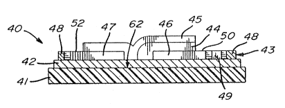
identified by the reference 40 in Figuxes 3 and 4 o~
the appended drawings~ ..
.
,: ,.
~, ~
.
. ~ , .
W094/28403 2 1 41 s 6 1 FCT/CA94/0031'
23
:
. .
Substrate 4l:
; As illustrated in Figures 3 and ~, this ~.'
~ sensor 40 comprises a substrate 41 made of a piece of
!, 5 crystalline silicon, glass, metal, ceramic, or plastic
material càpable of resisting to high~ temperatures
higher. Fabrication and operation~of the sensor 40 : -.
requires that the material of the~;substrate 41 be
capable of resisting to temperatures h;igher than 200 `
C, to water and water vapour, to any organic or ~`
inorganic chemical contaminants, and to dust '"
accumulation. '"~,'
, ;.
Ideally, the elastic constants (Young's ::'
15 modulus and Poisson's ratio) and the coeffic1ent of `~"
thermal expansion of the~ matexial fQrming the ~`'`.'
substrate 41 are nearly those of silicon or quartz to : '.
avoid cracking due to temperature :cycling and : .
ultimately problems of reliability and short-lifetime
20 of the sensor 40. ~ r`'~,
'~ ; : Thin film dieIect`ri.c material 42
.The first thin film 42, ~eposited on the~
:substrate 41, consists of dielectric material such as
SiO2. Use of other insulating materials, for example
i 'Si3N4, lmay~also be'contemplatedl. The'~functions~df:~he~ ~;
` thin ~ilm 42.are~to ensure:good adhesion between:the~
substrate~41 and:the~subsequent thin films '43-45,~ to~
' 30~ ensure~e1ectrical insulat:ion~between the subs~trate 41
and~ the- metallic~ thin~film 43, ~ and to~ provide ~ a~
diffusion~or alloy1ng~barrier between~the substrate:41
: :and the:;subsequent: metallic :thin film 43. The:thin : ':~
WOg4/2B403 PCT/CA94/00312
2~41S6~ , , '`;
t
, ~:~
film 42 has good thermal properties, in particular a
i~ good thermal expansion coefficient, and is chemically ~:
neutral so as not to react with gases to which the
~; de~ice is exposed, and so as to protect the substrate
42 from these gases.
Metallic thin film 43:
The thin film 43 is metallic and made of
pure metal such as platinum or other noble metal
deposited on the thin film of dielectric material 43. ;~
The metallic thin film 43 is divided into
four separate portions 46-49.
`~
Reference electrode 46:
The first thin film portion 46 is a thin ::~
film reference electrode whose function is to collect
electrical current. The thickness of the reference
electrode 4fi must be sufficient to make this ~lectrode ~
continuous (with no electrical interruptions) and :l.
conductive with a series resistance smaller than 10 Q.
It is important that the metallic electrode 46
25 contacts no other metallic thin film portions 37-39. ~:
'. ~ ' ,,`',
~ S_cond metallic electrode 47~
:: .
The second thin film:portion 47 forms a : :
1 30 second metallic electrode used, with the thin film
, reference electrode 46, to measure the electromotive
:force representative of the Co2 concentration.
, -
,:, .
: ~
!.'
.~ ;'.
., : : , :',
~}
~1 ~ ` : ' . '
':` ' ~ `
; :
` wos4l28403 21 ~15 61 PCT/CA94/00312
.. ` ' ' ' I ' ~ .
.,.
~Heating element 48:
'~Thin ~ilm portion 48 defines an open (see ' `
¦54) metallic peripheral loop constituting a heating -;
15 element. This heating element 48 is supplied~wi~h a ';-
'~current I. The thicknes~,~ width and length of the '~
heating element 48 are~adjusted~to~obtain a resistance~
'~ R adapted to an external current~;~souroe~supplying the~
~heating~'el~ment~ with~the current~ Power (I2R) is~ '
dissipated in the resistive heating~element 48 by the
Joule effect;to heat the sensor 40.~Accordingly, the ~
heating element 4~ loops around the sensor 40 at its ~ ~;';'
peri~hery in a simple or~ snaking ;configurat~ion as
required ~for~ efficient~ distri~ution~ of the~ heat~
15~ generated by the~current I.~
Inteqr~ted mioro-thermometer 49
Thin~film~port~i~on 49 constitute~a~micro~
20~ thermometer~integrated~to~the~thin film~ C02~ sensor~40;.
As illustrated~in'~Figure~'4;,~ the thin`film portion~49
~: .
defines` an~elong~ate~wire 59' having a temperature~
dependent~resistance~ t~o~enable ~measurement~o~f~;the~
t~mpe~atur~of~he~sensor~0
Ionic~conductor 44
A~thin~ lm; ~4 ~of~NASIC~N~ a3Zr2~i~Ol2)~
's de it d~ n~the'thi~ ilm ~referenc~e~electr e~46
30~ and~ a~p ''` ~ the ~s~'face~of ~he~hin~ lm~of~
ele ~ ~et~een the e~oc~rod~s 46~and~
' W094/28403 PCT/CA94/0~312
2141~61
26
.~ , .
... .
,include a plurality of layers which through their .
composition or structure serve to act as passivation,
~stabilisation and/or diffusion-barrier films. ;.
!5 Reactive CO sensltive lay~r 45: ~ ;
.'.. ~ .'
The last thin film 45, deposited on the
electrode 47, ~he surface portion of the thin film of .:
diele.ctric material 42 between the metallic electrode
47 and the thin film ionic conductor 44, is made of
sodium carbonate alone or stabilized by barium
carbonate to form a reactive thin film C2 sensltive :.
layer.
`'`
Mechanism of detection of sensor 40:
.:
The mechanism of detection used by the .
sensor 40 is exactly the same as described in relation `~
: .to the ~en~or 10 and, therefore, will not be further
.I 20 described in the present de~cription.
Fabrication of sensor 40:
The different steps conducted during
25 ~ fabrication of the thin film C2 sensor ~0 are
explained hereinafter. :-
~: ~ The surface 62 of the substrate 41 is
i ~first chemical~ly etched to clean this surface 62 prior :~.30 to thin film deposition. :~The substra~e 41 must be ~
- : :
:~ properly cleaned to~ avold :organic and inorganic ~-
: contamination (to:levels of p.p.m.~ of the thin layer .-~
: ~ 42 to be deposited. Such contamination may lead to
.
i~i ~
,,
~~ WQ94/28~03 PCTICA91/0031' ~.
21~1561
27 .:-
. reliability problems such as slow degradation of the '.'
: sensor 40.
. The thin film:of dielectric material 42 `.'
5 is tben deposited on the substrate 41 either by RF '."
reactive magnetron sputtering, or plasma enhanced or ;~.''
:normal chemical'vapour deposition. When the substrate '''.
is made of silicon, thermal oxidation of the silicon '.. :.
may be used to~produce the-insulating:thin film 4~
::lO directly on the surface of the substrate 41. ~ ~;
~ . ,; ' ~.',.
Platinum or another noble meta~ is .~.''
. . .
: deposited onto the:thin film of dielectric material 42
to form the thin film reference electrode~46, second
:15 thin film metallic electrode 47, heating element 48
: ~ and micro-thermometer 49.~ It can be deposited by~thin
film technigues including reactive evaporation in an
ultrahigh 'vacuum chamber,' RF reactive mag~etron
sputte~ing, ~:~electroplating, electrol~ess plating,:
20~ : screen~printing,`or plasma enhanced;or normal chemical
vapour~deposition.`
Use~of proximity~masking can be~used
'during'~depos:ition~to produce~from the s1ngle thin~film~
::; 25~ 43 the~ refer~ence electrode : 46, second metallic
~:'electrode~47, heating element 48~and micro-thermometer
`;j` !49.~ Al~ernat:ivelyj laser abl:at'~ion~canibelused td ~ut'
in~'the~;thin:film.43~the~:two el~ectrod:es~46 and 47,~ the~
. ~ h~ating;element:48:and~he:~'mlcr~o-thermometer~49.
Ionic~conductor material is sputt~ere~d ont~o~
the th;in:fi~lm~referen~e~e~lectrode~4~6~and a port~ion~of
the;~surface of~the thln~film of dlelectric materlal~42
WO94/284Q3 PCTiCA94/0031'
2141561 28
. ::
,j
~ .
between the two electrodes 46 and 47 to form the thin
film ionic conductor 44. The method for depositing
this thin film 44 is the same as for thin film 15 of
¦ sensor 10 (Figures 1 and 2).
~
Sodium carbonate a~one or stabilized by
barium carbonate i5 then deposited on the second thin -~
film metallic electrode 47, the thin film ionic
conductor 44 and th~ surface of the thin film 42 ` ;
~0 between the ionic conductor 44 and the electrode 47 to
form a reactive thin film Co2 sensitive layer. RF
magnetron sputtering can be used to deposit thin film
45. Other methods such as sol-gel coating, reactive
evaporation in an ultra high vacuum chamber, plasma
enhanced or normal chemical vapour deposition, etc.
can also be contemplated. ;~
To enable wiring~of the sensor 40 using
conventional bonding techniques, no material is
deposited on surface portion 50 of the thin film
reference electrode 46 whereby an electric wire 51 can
be connected ~hereto. Alsot no material is deposited
on surface portion 52 of the second thin film metallic
electrode 47 whereby an electric wire 53 (Figure 4) ,
can be connected thereto. As no material is deposited
on the thin ~ilm heating element 48 and micro
th~rmometer 49, electric wires 57~ and 58 can be
connected~to the ends 55 and~56 of the heating element
48, respectively, and electric wires 60 and 61 can be `
30 connected to the respectlve ends of the integrated ~`
micro-thermometer 49.
~' ~ : ., -.,
.~..
f1; . ,"':
~ : .~
....
W094/28403 21 ~15 61 PCT/CA94/0~31~ ~
29
Proximity masking can be used during :~
deposition of eiach thin film 42-45 to produce the
structure shown in Figures 3 and 4. :
~aser ablation of the thin films 42-45 may
also be used to give to the C02 sensor 40 the structure
o~ Figures 3 and 4. -
.-;
Finally, the substrate 41 is cut by means
of laser scribing, cleaving or diamond saw techniques,
or a combination of these techniques, and the thin
film C02 sensor 10 is then packaged using conventional
hybrid packaging techniques~
The thin film C02 sensor 10,40 ac¢ording
to the invention is capable of continuously detecting
and monitoring low concentrations of C02 with a
sensitivity of loO p.p.m. or less. It uses a solid
electrolyte and may be fabricated by means of thin
film techniques. The sensor o~ the invention has
numerous applications in the field of air quallty
control, biomedical monitoring and industrial
processes and control.
Several thin film C02 sensors 10,40 can be
mounted in cascade to increase the amplitude level of
the detected~electromotive force and `thereby/ impro~te
the C02 detection~ sensitiYity. Figure 5 illustrates
two thin ~ilm sensors 40~(Figures 3 and t4) mounted in
cascade. In this particular case, the thin film
rèference electrode of the first sensor and the second
thîn fllm metallic electrode of the second sensor form
: a common electrode 63. The peripheral thin film
. ~: ~
....
:
~ ' ',t''~
.' ''~
W094/28403 PCT/CA94/0031
2 1 ~15 6 1 30
'
, .
heating element 64 then surrounds the two sensors 40
mounted in cascade.
.
,Also, the thin film~CQ2 sensor lO, 40 can
!5 be provided with an outer CO2 permeable membrane. When
such a sensor lO is immersed in blood, the membrane
enables passage of Co2 through it to thereby allow the
sensor lO to sense the CO2 concentration in this blood.
lOAn electronic system (not shown) dedicated
to the conversion of the electromotive force (EMF)
between the two metallic electrodes to chemical
concentration of CO2, as well as to periodic self~
verification of the performance of the sensor lO,
regeneration of the ionic conductor thin film 15,
; thermostating the temperature of operation, auto-
recalibration etc. can be integrated to the substrate
11 along with the sensor 10,40. A smart
electrochemical gas sensor is then obtained~
Last of all, it should be pointed out that
the chemistry of the thin ~ilms 15,44 and 16,45 of the
sensor 10,40 in accordance with the present in~ention
can be modified to enable detection of the
concentration of gases other than C2
''
, ; ` Although the present invention hasibeen
described hereinabove by way of preferred embodiments ~-
i~ thereof, these embodiments~can be modi~ied at will,
`30 within the scope of the appended claim~, without
departing from thè spirit and~nature of thie subject
`~ invention.
?
.