Note: Descriptions are shown in the official language in which they were submitted.
DATA DEMODULATION CIRCUIT AND Il~ .OD FOR SPREAD Sr~l~U.I
COMMUNICATION
R~GRouNn OF T~ TNV~NTION
F;~l~ nf ~h~ Tnv~nt;nn
The present invention relates generally to a data demod-
ulation circuit and method for spread spectrum communication
and, more particularly, to a data demodulation circuit and
method capable of eliminating the influence of a carrier
offset remaining after detection by use of pilot signals
whose data are unmodulated transmitted from a cell-site. The
present invention is also directed to a data are demodulation
circuit and method designed to remove the interference caused
by pilot signals of different timings, and further to a data
demodulation circuit and method allowing a diversity recep-
tion through a plurality of such data demodulation circuits
and methods.
n~c~r;~t; nn nf th~. R~.l~t~ Art~
Direct sequence (DS) spread spectrum communication
systems (hereinafter referred to as SS system) has various
advantages such as immunity to interference and frequency
selective fading, multiple accessibility, and hence is being
developed as one of the communication systems for mobile
communications including mobile phones, cellular phones,
cordless phones and wireless LANs. In the following descrip-
tion, a term "symbol" will represent one of the information
CA2 ~ 4 i 654
alphabets to be decided by the data modulation scheme. In
the case of BPSK (binary shift keying) modulation, the symbol
can be considered to be data.
Fig. 31 depicts a schematic configuration of a mobile
unit telephone of CDMA ( code division multiple access) cellu-
lar telephone system disclosed in US Patent No. 5103459.
This mobile CDMD telephone system includes an antenna 1 being
connected via a diplexer 2 to an analog receiver 3 and a
power amplifier 4. The antenna 1 receives SS (spread spec-
trum) signals from a cell-site to provide received signals to
the analog receiver 3 through the diplexer 2. The analog
receiver 3 includes a down converter that converts the input
received signals to baseband signals which are in turn con-
verted to digital signals by an A/D ( analog to digital)
converter. Thus digitized baseband signals are fed to a
searcher receiver 5 and digital data receivers (or data
demodulator circuits) 6 and 7.
When the SS signals arrive at the receiver via a plural-
ity of paths, there will arise timing differences for each
signal of respective paths. The data demodulator circuits 6
and 7 are able to select which path signal is to be tracked
and received. In the presence of two data demodulator cir-
cuits as shown in Fig. 31, the two separate paths are tracked
in parallel.
On the contrary, in response to a control signal from a
control processor 8, the searcher receiver 5 scans a time
2 1 4 t 6 ~ ~r
domain in the vicinity of the reference timing of a received
pilot signal, so as to detect respective pilot signals con-
tained in the received multipath signals (signals received by
way of a plurality of paths) from the cell-site. Then, the
searcher receiver 5 compares the strength of the received
pilot signals, and outputs an strength signal to the control
processor 8 to indicate the strongest signals.
Then, the control processor 8 provides control signals
to the data demodulator circuits 6 and 7 for respective
processing of one of the different strongest signals.
The function of the data demodulator circuits 6 and 7 is
to correlate the received signals with the PN (pseudo noise)
codes used in the transmitter side. Fig 32 depicts the
detail of a data demodulator circuit disclosed in the U. S.
Patent No. 5103459. The data demodulator circuits 6 and 7
include PN generators 516 and 518 which generate PN codes
PNI(t) and PNQ(t) for the in-phase axis and the quadrature
axis respectively, corresponding to one of the received path
signals. The data demodulator circuits 6 and 7 each further
include a Walsh function generator 520 for generating a Walsh
function appropriate for the cell-site to communicate with
this mobile unit. The Walsh function generator 520 generates
a code sequence corresponding to Walsh function allocated in
response to the select signal from the control processor. `As
a part of a call set-up message, the select signal are trans-
mitted from a cell-site to the mobile unit. PN codes PNI(t)
2 1 4 1 6 ~ 4
and PNQ(t) output from the PN generators 516 and 518, respec-
tively, are provided as inputs to EX-OR gates 522 and 524,
respectively. The Walsh function generator 520 provides its
output to the EX-OR gates 522 and 524 which calculate EX-OR
to generate sequences PNI.(t) and PNQ.(t).
The sequences PNI.(t) and PNQ,(t)are input to PN QPSK
(quadrature phase shift keying) correlator 526 for process-
ing, and outputs of correlator 526, I and Q, are led into
corresponding accumulators 528 and 530. As a result, respec-
tive correlations with respect to the in-phase axis received
signals and the quadrature axis received signals are calcu-
lated by the cooperation of the PN QPSK correlator 526 and
the respective accumulators. The outputs of the accumulators
are provided to a phase rotator 532. The phase rotator 532
also receives the phase of a pilot signal from the control
processor 8. The phase of a received symbol is rotated in
response to the phase of the pilot signal. The phase of the
pilot signal is decided by the searcher receiver and the
control processor. The output of the phase rotator 532 is
in-phase axis data 23 to be fed into a combiner-decoder
circuit 9.
The combiner-decoder circuit 9 consists of a diversity
combiner circuit and an FEC decoder circuit.
The diversity combiner circuit adjusts the timing of two
received symbols into alignment, multiplies the two symbols
by values corresponding to their respective relative signal
~A2 1 41 65~
strength, and simultaneously adds them together. This opera-
tion results in a maximal ratio combining diversity recep-
tion. Reference is to be made to PCT/US90/06417 disclosing a
form of the diversity reception in the CDMA cellular system.-
As described hereinbefore, the conventional receiver hasa configuration in which all the path signals are processed
in common by the single analog receiver acting to down con-
vert the received signals to base band digital signals. It
is to be noted that the each received path signals has inde-
pendent carrier phases respectively. For a single path
signal, for example, COHERENT SPREAD SPECTRUM SYSTEMS, by
J.K.Holmes, John Wiley & Son discloses a manner of control-
ling the phase of the received signal in the analog receiver
3 with the aid of a carrier recovery circuit such as a Costas
loop. However, in the case of a plurality path signals, it
is difficult to simultaneously control the different phases
of a plurality of received path signals. Therefore, any
input signals to the data demodulators will inevitably con-
tain a phase difference (or a residual phase difference after
down converting) between a received path carrier and a local
carrier used for down converting.
More specifically, where the modulation by the data and
by the Walsh function for user identification are both BPSK
(bi-phase shift keying) and the modulation for spre~;ng is
QPSK (quadrature phase shift keying), in the same manner as
the modulation disclosed in the US Patent No. 5103459, then a
~.,
CA2141654
complex envelope of transmission signal S(t) can be given as
S(t) = W(t) [PNI(t) + jPNQ(t)]
= W(t) PNI + jW(t) PNQ(t)
= SI(t) + jSQ (t),
where W(t) is a multiplexing signal being multiplexed of
SS signals transmitting to each user and a pilot signal, and
let di(t), Wi(t) and ai be modulation data, a Walsh func-
tion, and a constant corresponding to power allocation, to i-
th user, respectively, and N be a number of multiplexing,
then W(t) is
W(t) = ~idi(t) Wi(t)
(~ represents the sum of i = O to N, and i = O corre-
sponds to a pilot signal)
Next, let p be a received amplitude of a received path
signal; and ~ be a phase difference (or a phase difference
after down converting) between a received path signal carrier
and local carrier used in down converting, then the complex
envelope RX(t) of one of the received path signal to be
demodulated at the output of the analog receiver can be
expressed as
RX(t) = pS(t) exp[j~]
= pW(t) [PNI(t) + jPNQ(t)]
* [cos~ + jsin~]
= pW(t) [{PNI(t) cos~ - PNQ(t) sin~ }
+ j{PNQ(t) cos~ + PNI(t) sin~}]
= RXI (t) + jRXQ(t)
~A2 1 4 1 ~4
Namely, the in-phase axis received signal RXI(t) is a
real part of RX(t), resulting in
RXI(t) = pW(t) {PNI(t) cos~ - PNQ(t) sin~}
and the quadrature axis received signal is an imaginary part
of RX(t), resulting in
RXQ(t) = pW(t) {PNQ(t) cos~ + PNI(t) sin~}.
These in-phase axis received signal and quadrature axis
received signal are provided as input to the PN QPSK correla-
tor.
In Fig. 32 the phase rotator 532 is used to eliminate
the influence of a phase difference. Although the US Patent
No. 5103459 does not disclose in detail a way of deciding a
pilot signal phase as the reference phase of the phase rota-
tor, the searcher receiver also includes a PN QPSK correlator
and accumulators associated with the pilot signal, whereby
that phase is supposedly determined through the execution of
an arithmetic tan~1(sin~ / cos~). Further, the phase rota-
tion operation may be considered as a product operation of
the phase compensation term exp (- j~) = cos~ - jsin~. Such
phase rotation operation will adversely result in a compli-
cated processing in which it is necessary to execute tan~l
arithmetic for finding ~ and to again find cos~ and sin~ from
thus obtained ~.
Further, owing to the scAnn;ng of a plurality of re-
ceived paths, the searcher receiver entailed a problem that
the reference phase is sensitive to the influence of noise
CA21 41 ~54
since the averaging time for reducing the influence of noise
is shortened in proportion to time period to be scanned, as
compared with the case where the phase is determined by a
single path signal. (In other words, as the noise is random,
a longer averaging time will reduce the influence of noise,
noise influence reducing effect will not be expected suffi-
ciently with a shorter averaging time). Disadvantageously, a
longer averaging time for ensuring a sufficient reduction of
noise effect would elongate the time required to obtain the
results of sc~nning over the entire time domains, resulting
that a true phase difference may not be found due to a varia-
tion of link condition depending on the movement of the
mobile during the elongated time.
While on the contrary, Japanese Patent Application No.
149369/93 discloses a data demodulator circuit in which a
pilot signal, cont~ine~ in a specific received path signal
demodulated by the data demodulator circuit, is subjected to
a correlating process to extract phase difference information
for compensating the influence of a phase difference. Fig.
33 depicts a phase difference information extracting section
and a phase compensating section constituting the data demod-
ulator circuit disclosed in the Japanese Patent Application
No. 149369/93. In Fig. 33, reference numerals 20a, 20b, 20c
and 20d denote averaging sections each acting to perform a
time averaging operation with respect to input signals.
These sections subject in-phase axis received signal and
C~141654
quadrature axis received signal to processing depicted in the
diagram to thereby provide, as averaging section outputs,
components paO cos~ or paO sin~ associated with a phase
difference.
aO represents a constant related to a power allocation
of the pilot signal. It is to be appreciated that time
averaging operations excee~ing one symbol time performed by
the averaging sections ensure a sufficiently suppressed
influence of the cross-correlation between PNI and PNQ con-
tained in the outputs of multipliers 11, 12, 13 and 14.
Since a received signal in the presence of a phase
difference is defined as RX(t) = pS(t) exp[j~] as described
earlier, the influence of the phase difference can be cleared
by multiplying RX(t) by a phase compensation term exp[-j~],
which yields
pS(t) exp[j~] exp [-j~] = pS(t)
pSI(t) + jpSQ(t).
Here, if the received signal is separated into an in-phase
axis received signal and a quadrature axis received signal
previous to the multiplication of the phase compensation
term, the above expression can be written as
pS(t) exp[j~] exp [-j~]
= [RXI(t) + jRXQ(t)] * exp[-j~]
= [RXI(t) + jRXQ(t)] * [cos~ - jsin~]
= [RXI(t) cos~ + RXQ(t) sin~]
+
4 ~ 6 ~ 4
j[RXQ(t) cos~ - RXI(t) sin~]
Namely, taking notice of the right side of the above
expression, a first term is in the form of the sum of a term
obtained by multiplying the in-phase axis received signal by
cos~ and a term obtained by multiplying the quadrature axis
received signal by sin~, whereas a second term is comprised
of the sum of a product of the in-phase axis received signal
and
-sin~ and a product of the quadrature axis received signal
and
cos~. On the other hand, the outputs of the averaging sec-
tions mean 20a, 20b, 20c and 20d are respectively paOcos~, -
paOsin~, paOsin~ and paO cos~. Accordingly, without the
coefficient
paO signal processing equivalent to the above expression will
be implemented by multiplying the outputs of the averaging
sections mean 20a, 20b, 20c and 20d, and RXI and RXX together
in such a combination as depicted in Fig. 33 and then taking
addition or subtraction on the products.
In Fig. 33, two components on cos~ are respectively
derived from the averaging sections mean 20a and 20d, and two
components on sin~ are respectively derived from the averag-
ing sections mean 20b and 20c. Fi~. 34 depicts a phase
compensating section of the data demodulator circuit also `
disclosed in the Japanese Patent Application 149369/93.
Aiming at simplifying the circuitry, the phase compensating
", 10
r ~
CA2, 4 i 654
section is provided with a single multiplier and a single
averaging section inte~e~ to extract ln cooperation the
components on cosfl and sin~.
In this ~n~er~ Fig. 32 configuration inconveniently
necessitated such complicated processing as tan~1 arithmetic
and phase rotation operation, or the reference phase was
sensitive to the noise effect due to the use of a pilot phase
presented by the searcher receiver sc~nning a plurality of
received pilot signals. The circuit of Fig. 33 still re-
mained redundant structure regardless of its intention to
overcome these problems. Although the configuration depicted
in Fig. 34 contrives to remove the redundancy of the Fig. 33
configuration, it has left unsolved the problem of being
sensitive to the influence of the noise, due to its use of
only half of the components associated with the phase dif-
ference information cont~ine~ in the received signals.
Also, the use of a plurality of data demodulator cir-
cuits for diversity reception may bring about a problem that
the complexity of the receiver as a whole is increased ac-
cordingly as the configurations and processing of individual
data demodulator circuits become more complicated.
Moreover, increased influence of the noise of the phase
compensation means constituting the data demodulator circuit
will cause a deterioration in the demodulation characteris-
tics of the data demodulator circuit. Thus, there arises a
problem of improving the demodulation characteristics of the
C~2141654
individual data demodulator circuits to ensure further im-
proved demodulation characteristics in the diversity recep-
tion.
Furthermore, in order to get the maximum performance of
the maximal ratio combining diversity reception, it is neces-
sary for
the phases of the outputs of respective data demodulator
circuits to adjust the phases accurately and weighted by
values in response to the signal strength. However, the use
of a pilot signal phase and a pilot signal level obtained by
the searcher receiver would be difficult to get the maximum
performance of the diversity reception due to larger in-
fluence of noise. "To adjust the phases" means herein that
the phase compensation is carried out accurately.
Also, there may be a frequency deviation generally
between a transmission carrier frequency for use in a cell-
site transmitter and a local oscillator output frequency used
in down converting within the mobile.
The above-described phase difference ~ remaining after
down converting can be considered to have no time variation,
while if there is the frequency deviation between the re-
ceived path signal carrier and the local oscillator output
used in down converting, it can ~e expressed as
~ = &wt + ~ `
where ~ = 2~f, and ~f is a frequency deviation. Hereinafter,
~ represented in the above expression will be referred to as
- 12
CA2 14 16~4
a carrier offset.
Due to the random behavior of the noise, an elongated
averaging time in the averaging sections would reduce the
influence of the noise but adversely prevent the compensation
of carrier offset (frequency and phase compensation) owing to
the time variation for ~. A shorter time T would result in
less influence of ~ but also in a shortened averaging time
which will in turn suppress the noise reduction effect by
averaging. Thus, the ~onventional phase compensation means
allows the problem of increased influence of noise to remain
unsolved.
Besides, as the phase compensation means of the data
demodulator circuit is increasingly infll)~nc~ by the noise,
the demodulation characteristics of the data demodulator
circuit will be degraded. Thus, there - ~ins the problem of
improving the demodulation characteristics of individual data
demodulator circuit to get the further im~Lovement of the
demodulation characteristics of the diversity reception.
Also there remains the problem of adjusting the phase of the
outputs of the respective data demodulator circuits to get
the sufficient performance of the diversity reception.
A means of compensating the carrier offset has been, for
example, reported by Takahashi, Takeishi and Onishi (IEICE,
Spring National Conference A-204, 1993) (although its modula-
tion method differs from that of the US Patent No. 5103459).
To obtain a fixed phase difference, this method comprises the
13
CA~ I 4 ' 654
steps of performing a tan~l arithmetic for each despre~;ng
symbol to find a phase for each symbol and the differences
between the successive phases, averaging the differences to
find the amount of phase rotation corresponAing to the fre-
quency offset, and subtracting therefrom the amount of phase
rotation correspon~ing to the phase found for each symbol, in
order to finally average the results.
Namely, let ~ (n) be a phase derived from an n-th des-
preading symbol, T be a symbol duration, N be an averaging
number, and ~ = ~T, then ~ and ~ are obtained by an opera-
tion
~(n) = tan~l[sin{~(n)} / cos{~(n)}]
= (1 / N)~(n + 1) - ~(n)]
~ = (1 / N)~[~(n) - n~]
where ~ represents the sum of N = 1 to N. Then, the des-
preading
symbols (which correspond to the outputs of the accumulators
528 and 530 in Fig. 32) are multiplied by exp(-j~). Never-
theless, it will be necessary to operate tan~l and phase
rotation, resulting in complicated processing.
Also, in the case of a diversity reception using a
plurality of data demodulator circuits, complicated process-
ing required for the individual data demodulator circuit will
inconveniently bring about a further increased complexity in
the receiver as a whole.
Besides, the use of the communication system disclosed
14
CA2 1 41654
in the US Patent No. 5103459 will allow a problem that the
received multipath signals cause mutual interferences to
degrade the receiving characteristics. More specifically,
when signals transmitted from the cell-site are received
through a plurality of paths, there will arise differences in
the timing of the reception of the respective path signals.
S(t) being orthogonal multiplexed signals based on a Walsh
function, the orthogonality of the orthogonal multiplexed
signals is permitted to be established only when respective
receive timings coincide, whereas if the receive timings are
individually different, they will become
interference components to degrade the demodulation charac-
teristics. Accordingly, there remains a problem of improving
the degradation in the demodulation characteristics of the
data demodulator circuit by the interference components.
There also remains the problem of reducing the degrada-
tion in the demodulation characteristics of the individual
data demodulator circuit by the interference components to
further improve the demodulation characteristics of the
diversity reception.
~UMMA~Y OF T~ TNV~NTTON
The present invention was conceived in view of the
problems involved in the prior art described above.
It is therefore one object of the present invention to
provide a data demodulator circuit for spread spectrum commu-
nication having a simpler configuration capable of eliminat-
~A2 1 4 1 654
ing a carrier offset remaining after down converting tothereby improve its demodulation characteristics.
Another object of the present invention is to provide a
data demodulator circuit for spread spectrum communication
ensuring improved demodulation characteristics by removing
the interference caused by pilot signals with different
timing.
Still another object of the present invention is to
provide a data demodulator circuit for spread spectrum commu-
nication having a simple configuration capable of a diversity
reception with the aid of a plurality of the data demodula-
tion circuits to thereby further improve its demodulation
characteristics.
According to a first aspect of the present invention, in
order to accomplish the above object, a data demodulator
circuit for spread spectrum communication, demodulating data
from received signal which is spread spectrum modulated with
respect to the in-phase axis and the quadrature axis by a
direct sequence techniques with an in-phase axis pseudo noise
code and a quadrature axis pseudo noise code, respectively,
said data demodulator circuit comprises a phase difference
information extraction means for extracting information of
phase differences, by multiplying in-phase axis received
signal and quadrature axis received signal with respectivè
pseudo noise codes used on the transmitter side, taking
addition or subtraction on two of the products in a predeter-
CA2141654
mined combination, and averaging the results of the additionor subtraction a phase compensation means for compensating
the effect of phase differences rem~i ni ng in the in-phase
axis received signal and the quadrature axis received signal,-
by use of the phase difference information obtained by said
phase difference information extraction means; and a data
demodulation means for demodulating transmitted data from the
outputs of said phase compensation means.
According to a second aspect of the present invention,
in order to accomplish the above object, a data demodulator
circuit for spread spectrum communication, demodulating data
from received signal which is spread spectrum modulated with
respect to the in-phase axis and the quadrature axis by a
direct sequence techniques with an in-phase axis pseudo noise
code and a quadrature axis pseudo noise code, respectively,
said data demodulator circuit comprises a plurality of data
demodulator circuits with independent timing for spread
spectrum communication according to claim l; a timing adjust-
ment means adjusting the timing of the outputs of a plurality
of said data demodulator circuits; an adder means for adding
the outputs of said timing ad;ustment means; and a data
decision means for deciding the transmitted data from the
output of said adder means.
According to a third aspect of the present invention,`in
order to achieve the above object, a data demodulator circuit
for spread spectrum communication, demodulating data from
C,~2I47654
received signal which is spread spectrum modulated with
respect to the in-phase axis and the quadrature axis by a
direct sequence techniques with an in-phase axis pseudo noise
code and a quadrature axis pseudo noise code, respectively,
said data demodulator circuit comprises a phase difference
information extraction means for extracting information of
phase differences, by multiplying in-phase axis received
signal and quadrature axis received signal by respective
pseudo noise codes used on the transmitter side, taking
addition or subtraction on two of the products in a predeter-
mined combination, and averaging the results of the addition
or subtraction: a delay means for delaying the in-phase axis
received signal and the quadrature axis received signal for a
suitable period of time; a frequency and phase compensation
means for compensating the effect of frequency and phase
offset remaining in the in-phase axis received signal and the
quadrature axis received signal with time delayed by said
delay means, by use of the phase difference information
obtained by said phase difference information extraction
means; and a data demodulation means for demodulating trans-
mitted data from the outputs of said frequency and phase
compensation means.
According to a fourth aspect of the present invention,
in order to attain the above object, a data demodulator
circuit for spread spectrum communication, demodulating data
from received signal which is spread spectrum modulated with
18
C~2 1 4 1 654
respect to the in-phase axis and the quadrature axis by a
direct sequence t~chniques with an in-phase axis pseudo noise
code and a quadrature axis pseudo noise code, respectively,
said data demodulator circuit comprises a plurality of data
demodulator circuits with independent timing for spread
spectrum communication according to claim 3; a timing adjust-
ment means adjusting the timing of the outputs of a plurality
of said data demodulator circuits; an adder means for ~ing
the outputs of said timing adjustment means; and a data
decision means for deciding the transmitted data from the
output of said adder means.
According to a fifth aspect of the present invention,
provided in order to accomplish the above object, a data
demodulator circuit for spread spectrum communication, demod-
ulating data from received signal which is spread spectrum
modulated with respect to the in-phase axis and the quadra-
ture axis by a direct sequence techniques with an in-phase
axis pseudo noise code and a quadrature axis pseudo noise
code, respectively, said data demodulator circuit comprises a
phase difference information extraction means for extracting
information of phase differences, by multiplying in-phase
axis received signal and quadrature axis received signal by
respective pseudo noise codes used on the transmitter side,
taking addition or subtract on two of the products in a
predetermined combination, and averaging the results of the
ddition or subtraction; a delay means for delaying the in-
t~ ~ 19
CA 2 1 4 1 654
phase axis received signal and the quadrature axis receivedsignal for a suitable period of time; a level control means
for controlling the levels of the phase difference informa-
tion obtA;ne~ by said phase difference information extraction
means; a frequency and phase compensation means for compen-
sating the effect of frequency and phase offset remaining in
said time delayed in-phase axis received signal and quadra-
ture axis received signal, by use of the phase difference
information whose level has been controlled by said level
control means; and a data demodulation means for demodulating
transmitted data from the outputs of said frequency and phase
compensation means.
According to a sixth aspect of the present invention,
provided in order to accomplish the above object is a data
demodulator circuit for spread spectrum communication,
demodulating data from received signal which is spread spec-
trum modulated with respect to the in-phase axis and the
quadrature axis by a direct sequence techniques with an in-
phase axis pseudo noise code and a quadrature axis pseudo
noise code, respectively, said data demodulator circuit
comprises a plurality of data demodulator circuits with
independent timing for spread spectrum communication accord-
ing to claim 5; a timing adjustment means adjusting the
timing of the outputs of a plurality of said data demodulator
circuits;
a level adjustment means for adjusting the levels of said
,?- ~ 20
.~
CA21 4 7 654
outputs of said plurality of data ~ :dulator circuits with
timing adjusted by said timing adjustment means; an adder
means for adding the outputs of said level adjustment means;
and a data decision means for deciding the transmitted data
from output of said adder means.
According to a seventh aspect of the present invention,
provided in order to attain the above object is a data demod-
ulator circuit for spread spectrum communication, demodulat-
ing data from received signal which is spread spectrum modu-
lated with respect to the in-phase axis and the quadrature
axis by a direct sequence techniques with an in-phase axis
pseudo noise code and a quadrature axis pseudo noise code,
respectively, said data demodulator circuit comprises a phase
difference information extraction means for extracting infor-
mation of phase differences, by multiplying in-phase axis
received signal and quadrature axis received signal by re-
spective pseudo noise codes used on the transmitter side,
taking addition or subtraction on two of the products in a
predetermined combination, and averaging the results of the
addition or subtraction; a delay means for delaying the in-
phase axis received signal and the quadrature axis received
signal for a suitable period of time; a frequency and phase
compensation means for compensating the effect of frequency
and phase offset remaining in said time delayed the in-phase
axis received signal and the quadrature axis received signal
with time delayed by said delay means, by use of the phase
21
,. . .
CA2 141 654
difference information obtAine~ by said phase difference
information extraction means; an interference amount calcula-
tion means for calculating the amounts of interference ef-
fecting on the outputs of said frequency and phase compensa-
tion means due to pilot signals with different timing; and a
data demodulation means with c~ncel er for demodulating trans-
mitted data from the outputs of said frequency and phase
compensation means, while subtracting the interference
amounts calculated by said interference amount calculation
means.
According to a eighth aspect of the present invention,
provided in order to attain the above object is a data demod-
ulator circuit for spread spectrum communication, demodulat-
ing data from received signal which is spread spectrum modu-
lated with respect to the in-phase axis and the quadrature
axis by a direct sequence tP.chn;ques with an in-phase axis
pseudo noise code and a quadrature axis pseudo noise code,
respectively, said data demodulator circuit comprises a
plurality of data ~ ~dulator circuits with independent
timing for spread spectrum communication according to claim
7; a timing ad;ustment means adjusting the timing of the
outputs of a plurality of said data demodulator circuits; an
adder means for adding the outputs of said timing adjustment
means; and a data decision means for deciding the transmitted
data from the output of said adder means.
According to a ninth aspect of the present invention,
22
CA21 41 654
provided in order to attain the above object is a data demod-
ulator circuit for spread spectrum communication, demodulat-
ing data from received signal which is spread spectrum modu-
lated with respect to the in-phase axis and the quadrature
axis by a direct sequence techniques with an in-phase axis
pseudo noise code and a quadrature axis pseudo noise code,
respectively, said data demodulator circuit comprises a phase
difference information extraction means for extracting infor-
mation of phase differences, by multiplying in-phase axis
received signal and quadrature axis received signal by re-
spective pseudo noise codes used on the transmitter side,
taking addition or subtraction on two of the products in a
predetermined combination, and averaging the results of the
addition or subtraction; a delay means for delaying the in-
phase axis received signal and the quadrature axis received
signal for suitable period of time; a frequency and phase
compensation means for compensating the effect of frequency
and phase offset remaining in the in-phase axis received
signal and the quadrature axis received signal with time
delayed by said delay means, by use of the phase difference
information obt~ine~ by said phase difference information
extraction means; a level detection means for detecting the
levels of the phase difference information extracted by said
phase difference information extraction means; a selective
interference amount calculation means for calculating the
amounts of interference effecting on the outputs of said
23
~ A 2 1 4 1 6~
frequency and phase compensation means due to pilot signals
with different timing, controlling the results of said calcu-
lation in response to the levels detected by said level
detection means, and selectively outputting the amounts of
interference according to the results of said control; and a
data demodulation means with canceler for demodulating trans-
mitted data from the outputs of said frequency and phase
compensation means, while subtracting the interference
amounts calculated by said selective interference amount
calculation means.
According to a tenth aspect of the present invention,
provided in order to attain the above object is a data demod-
ulator circuit for spread spectrum communication, demodulat-
ing data from received signal which is spread spectrum modu-
lated with respect to the in-phase axis and the quadrature
axis by a direct sequence techniques with an in-phase axis
pseudo noise code and a quadrature axis pseudo noise code,
respectively, said data demodulator circuit comprises a
plurality of data demodulator circuits with independent
timing for spread spectrum communication according to claim
9; a timing ad;ustment means adjusting the timing of the
outputs of a plurality of said data demodulator circuits; an
adder means for adding the outputs of said timing adjustment
means; and a data decision means for deciding the transmitted
data from the output of said adder means.
According to a eleventh aspect of the present invention,
24
C A2 1 4 1 654
provided in order to attain the above ob;ect is 11. A data
demodulator circuit for spread spectrum communication, demod-
ulating data from received signal which is spread spectrum
modulated with respect to the in-phase axis and the quadra-
ture axis by a direct sequence techn; ques with an in-phase
axis pseudo noise code and a quadrature axis pseudo noise
code, respectively, said data demodulator circuit comprises a
phase difference information extraction means for extracting
information of phase differences, by multiplying in-phase
axis received signal and quadrature axis received signal by
respective pseudo noise codes used on the transmitter side,
taking addition or subtraction on two of the products in a
predetermined combination, and averaging the results of the
addition and subtract; a delay means for delaying the in-
phase axis received signal and the quadrature axis received
signal for suitable period of time; a level control means for
controlling the levels of the phase difference information
obt~;ne~ by said phase difference information extraction
means; a frequency and phase compensation means for compen-
sating the effect of frequency and phase offset remaining in
the in-phase axis received signal and the quadrature axis
received signal with time delayed by said delay means, by use
of the phase difference information obt~ine~ by said phase
difference information extraction means; an interference
amount calculation means for calculating the amount of inter-
ference effecting on said level controlled outputs of said
CA 2 1 4 1 6~4
frequency and phase compensation means due to pilot signals
with different timing due to signals with different timing;
and a data demodulation means with canceler for demodulating
transmitted data from the outputs of said frequency and phase
compensation means, while subtracting the interference
amounts calculated by said interference amount calculation
means.
According to a twelfth aspect of the present invention,
provided in order to attain the above object is a data demod-
ulator circuit for spread spectrum communication, demodulat-
ing data from received signal which is spread spectrum modu-
lated with respect to the in-phase axis and the quadrature
axis by a direct sequence techniques with an in-phase axis
pseudo noise code and a quadrature axis pseudo noise code,
respectively, said data demodulator circuit comprises a
plurality of data demodulator circuits with independent
timing for spread spectrum communication according to claim
11; a timing adjustment means adjusting the timing of the
outputs of a plurality of said data demodulator circuits; a
level adjustment means for adjusting the levels of said
outputs of said plurality of data demodulator circuits with
timing adjusted by said timing adjustment means; an adder
means for adding the outputs of said level adjustment means;
and a data decision means for deciding the transmitted datà
by the output of said adder means.
According to a thirteenth aspect of the present inven-
26
CA21 4 1 654
tion, provided in order to attain the above object is a datademodulator circuit for spread spectrum communication, demod-
ulating data from reeived signal which is spread spectrum
modulated with respect to the in-phase axis and the quadra-
ture axis by a direct sequence techniques with an in-phase
axis pseudo noise code and a quadrature axis pseudo noise
code, respectively, said data demodulator circuit comprises a
phase difference information extraction means for extracting
information of phase differences, by multiplying in-phase
axis received signal and quadrature axis received signal by
respective pseudo noise codes used on the transmitter side,
taking addition or subtraction on two of the products in a
predetermined combination, and averaging the results of the
addition or subtraction; a delay means for delaying the in-
phase axis received signal and the quadrature axis received
signal for suitable period of time; a level control means for
controlling the levels of the phase difference information
obt~;ne~ by said phase difference information extraction
means;
a frequency and phase compensation means for compensating the
effect of frequency and phase offset remaining in the in-
phase axis received signal and the quadrature axis received
signal with time delayed by said delay means, by use of the
phase difference information obtAine~ by said phase dif-
ference information extraction means; a selective interfer-
ence amount calculation means for calculating the amounts of
27
CA2 1 4 1 654
interference effecting on the outputs of said frequency and
phase compensation means due to pilot signals with different
timing, controlling the results of said calculation in re-
sponse to the levels detected through a controlled variable
calculation process by said level detection means, and selec-
tively outputting the amounts of interference in compliance
with the results of said control; and a data demodulation
means with ~.A~c~ler for demodulating transmitted data from
the outputs of said selective frequency and phase compensa-
tion means, while subtracting the interference amounts calcu-
lated by said interference amount calculation means.
According to a fourteenth aspect of the present inven-
tion, provided in order to attain the above object is a data
demodulator circuit for spread spectrum communication, demod-
ulating data from received signal which is spread spectrum
modulated with respect to the in-phase axis and the quadra-
ture axis by a direct sequence techniques with an in-phase
axis pseudo noise code and a quadrature axis pseudo noise
code, respectively, said data demodulator circuit comprises a
plurality of data demodulator circuits with independent
timing for spread spectrum communication according to claim
13; a timing adjustment means adjusting the timing of the
outputs of a plurality of said data demodulator circuits;
a level adjustment means for adjusting the levels of said `
outputs of said plurality of data demodulator circuits with
timing adjusted by said timing adjustment means; an adder
` 28
~A21 4 1 ~54
means for adding the outputs of said level adjustment means;
and a data decision means for deciding the transmitted data
from the output of said adder means.
According to a fifteenth aspect of the present inven-
tion, provided in order to attain the above object is a
method for data demodulation in a demodulation apparatus for
spread spectrum communication which demodulates data from
received signal which is spread spectrum modulated with
respect to the in-phase axis and the quadrature axis by a
direct sequence techn;que with an in-phase axis pseudo noise
code and a quadrature axis pseudo noise code, respectively,
said method comprises the steps of
multiplying in-phase axis received signal and quadrature axis
received signal with respective pseudo noise codes used on
the transmitter side; taking addition or subtraction on two
of the products in predetermined combination; extracting
information of phase differences by averaging the results of
the addition or subtraction; and compensating the effect of
phase differences remaining in the in-phase axis received
signal and the quadrature axis received signal by use of the
phase difference information.
According to a sixteenth aspect of the present inven-
tion, provided in order to attain the above object is the
method of data demodulation of claim 15, further comprising
before the compensating step, the step of: delaying the in-
phase axis received signal and the quadrature axis received
CA2141 654
signal for a suitable period of time; and wherein the compen-
sating step compensates the effect of frequency and phase
offset remaining in the in-phase axis received signal and the
quadrature axis received signal with time delayed by the
quadrature axis received signal with time delayed by the
delaying step, by use of the phase difference information.
According to a seventeenth aspect of the present inven-
tion, provided in order to attain the above object is the
method of data demodulation of claim 16, further comprising
before the compensating step, the step of: controlling the
levels of the phase difference information.
According to a eighteenth aspect of the present inven-
tion, provided in order to attain the above object is the
methods of data demodulation of claim 16, further comprising
the steps of:
calculating the amounts of interference effecting on the
frequency and phase compensation due to pilot signals with
different timing; and demodulating transmitted data by sub-
tracting the interference amounts.
According to a nineteenth aspect of the present inven-
tion, provided in order to attain the above object is the
method of data demodulation of claim 18, further comprising
before the calculating step, the step of: detecting the
levels of the phase difference information; selecting the
amounts of interference according to the levels of the phase
difference information.
CA21 $1 654
According to a twelfth aspect of the present invention,
provided in order to attain the above object is the method of
data demodulation of claim 18, further comprising before the
compensating step, the step of: controlling the levels of the
phase difference information.
According to a twenty-first aspect of the present inven-
tion, provided in order to attain the above object is the
method of data demodulation of claim 20, further comprising
before the demodulating step, the step of: selecting the
amounts of interference according to the levels of the phase
difference information.
According to a twenty-second aspect of the present
invention, provided in order to attain the above object is
the method of data demodulation of claim 15, further compris-
ing the steps of: adjusting the timing of outputs of a plu-
rality of the demodulation apparatus; ~ing the outputs of a
plurality of the demodulation apparatus; and deciding the
transmitted data.
RRTFF nF.~:CRT PTTON OF T~F nRAl~
These and other objects and advantages of the present
invention will become more apparent, when viewed in conjunc-
tion with the following drawings, in which
Fig. 1 is a configurational diagram of a data demodulà-
tor circuit in accordance with an embodiment of the present
invention;
CA21 41 6~4
Fig. 2 is a configurational diagram of an averaging
section;
Fig. 3 depicts a configuration of a data demodulator
circuit in accordance with another embodiment;
Fig. 4 depicts a configuration of a diversity combiner
circuit;
Fig. 5 illustrates a data demodulator circuit configured
in accordance with a further embodiment;
Fig. 6 illustrates a data demodulator circuit configured
in accordance with still another embodiment;
Fig. 7 is a configurational diagram of a data demodula-
tor circuit in accordance with a still further embodiment;
Fig. 8 is a configurational diagram of a controlled
variable calculating section;
Fig. 9 depicts a configuration of a data demodulator
circuit in accordance with yet another embodiment;
Fig. 10 depicts a configuration of a data demodulator
circuit in accordance with a yet further embodiment;
Fig. 11 illustrates a data demodulator circuit config-
ured in accordance with yet still another embodiment;
Fig. 12 illustrates a data demodulator circuit config-
ured in accordance with a yet still further embodiment;
Fig. 13 is a con~igurational diagram of an interference
amount calculating section;
Fig. 14 is a configurational diagram of a data demodula-
tor circuit in accordance with another embodiment of the
CA2 1 41 654
present invention;
Fig. 15 depicts a configuration of a data demodulator in
accordance with still another embodiment;
Fig. 16 depicts a configuration of a data demodulator in
accordance with yet another embodiment;
Fig. 17 illustrates a data demodulator circuit config-
ured in accordance with yet still another embodiment;
Fig. 18 illustrates a configuration of a level detector;
Fig. 19 is a configurational diagram of another inter-
ference amount calculating section;
Fig. 20 is a configurational diagram of a data demodula-
tor circuit in accordance with a further embodiment;
Fig. 21 depicts a configuration of a data demodulator
circuit in accordance with a still further embodiment;
Fig. 22 depicts a configuration of a data demodulator
circuit in accordance with a yet further embodiment;
Fig. 23 illustrates a data demodulator circuit config-
ured in accordance with a yet still further embodiment;
Fig. 24 illustrates a configuration of a further inter-
ference amount calculating section;
Fig. 25 is a configurational diagram of a data demodula-
tor circuit in accordance with another embodiment of the
present invention
Fig. 26 is a configurational diagram of a data demodula-
tor circuit in accordance with a further embodiment;
Fig. 27 depicts a configuration of another diversity
33
CA214 1 ~s4
combiner circuit;
Fig. 28 depicts a configuration of a data demodulator
circuit in accordance with still another embodiment;
Fig. 29 illustrates a configuration of still another
interference amount calculating section;
Fig. 30 is a diagram for illustrating a symbol timing;
Fig. 31 is a block diagram of a ~o~lvel,tional transmit-
ter-receiver;
Fig. 32 is a configurational diagram of a data demodula-
tor circuit employed in the conventional transmitter-
receiver;
Fig. 33 shows a configuration of a phase difference
information extracting section and a phase compensating
circuit constituting another conventional apparatus; and
Fig. 34 shows a configuration of a phase difference
information extracting section and a phase compensating
circuit contained within a further conventional apparatus.
n~cRTpTToN OF TH~ pR~F~RR~n ~MRonTM~T~
Exemplary embodiments of a data demodulator circuit for
spread spectrum communication in accordance with the present
invention will now be described with reference to the accom-
panying drawings.
~mh~m~
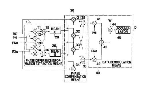
Referring first to Fig. 1 of the drawings, depicted is a
data demodulator circuit configured in accordance with the
34
CA21 41 654
present invention. In Fig. 1, input to a phase difference
information extraction means generally designated at 10 are
an in-phase axis received signal RXI and quadrature axis
received signal RXQ along with an in-phase axis pseudo noise-
code PNI and an quadrature axis pseudo noise code PNQ, from
which is extracted information of phase difference by averag-
ing sections meanC 20 and meanS 25. A phase compensation
means 30 makes use of the thus extracted phase difference
information to compensate for the influence of the phase
difference remaining on RXI(t) and RXQ(t) after down convert-
ing, and outputs phase ~ ensated in-phase axis component
and quadrature axis component. In a data demodulation means
generally designated at 40, the in-phase axis component and
quadrature axis component are respectively multiplied by the
in-phase pseudo noise code PNI and quadrature pseudo noise
code PNQ, and the respective products are added together
through an adder 43. Then, the output of the adder 43 is
multiplied by a Walsh function assigned to a mobile, and the
product is accumulated for a symbol duration through an
accumulator 45. It is to be noted throughout this specifica-
tion that the output of the accumulator 45 is provided to a
data decision means for deciding the data, or alternatively
provided to a diversity combiner circuit and, after the
diversity reception, further to the data decision means. `
A more detailed action of the data demodulator circuit
depicted in Fig. 1 will be described below. It is to be
CA21 41 654
appreciated that since among the previously mentioned objects
of the present invention the ob;ect to be achieved herein
lies in conveniently compensating the phase difference 0
re~; n; ng after the detection with a simple configuration,
description is made of a case where ~ is sufficiently small
~ ). Consideration will be given only to a path signal
which the data demodulator circuit is tracking and receiving
although a plurality of received path signal are contained in
the in-phase axis received signal and the quadrature axis
received signal. It is reported that the interference caused
by the received path signals having different timing behaves
like a Gaussian noise (at the accumulator output) upon demod-
ulation (written by Allen Salmasi and Klein S. Gilhousen,
entitled ON THE SYSTEM DESIGN ASPECTS OF CODE DIVISION MULTI-
PLE ACCESS (CDMA) APPLIED TO DIGITAL CELLULAR AND PRESONAL
COMMUNICATIONS NETWORKS, 41st IEEE Vehicular Technology
Conference).
As discussed earlier in the related arts, the in-phase
axis received signal RXI(t) and quadrature axis received
signal RXQ(t) are respectively written as:
RXI(t) = pW(t) {PNI(t) cos~ - PNQ(t) sin~}
RXQ(t) = pW(t) {PNQ(t) cos~ + PNI(t) sin~}
The outputs of multipliers 11 and 13 are respectively ex-
pressed as RXI(t) PNI(t) and RXQ(t) PNQ. Therefore, since`
PNI2(t) = PNQ2(t) = 1, the output of an adder 15 is
.
RXI(t) PNI(t) + RXQ(t) PNQ(t)
.. - 36
CA 2 1 4 ! 654
= pW(t) {PNI(t) cos~ - PNQ(t) sin~} PNI(t)
+
pW(t) {PNQ(t) cos~ + PNI(t) sin~} PNQ(t)
= 2pW(t) cos~
Similarly, the outputs of the multipliers 12 and 14 are
represented as - RXI(t) PNQ(t) and RXQ(t) PNI, respectively.
Hence, the output of an adder 16 will result in
RXQ(t) PNI(t) - RXI(t) PNQ(t)
= pW(t) {PNQ(t) cos~ + PNI(t) sin~} PNI(t)
pW(t) {PNI(t) cos~ - PNQ(t) sinO} PNQ(t)
= 2pW(t) sin~
The outputs of the adder 15 and 16 are provided as
inputs to the averaging sections meanC 20 and meanS 25 re-
spectively. As compared with the conventional configurations
depicted in Fig. 33 and 34, cos~ extracted components and
sin~ extracted components are respectively added coherently
(or in the same direction on vectror) by the adders prior to
inputting to the averaging sections. On the contrary, noise
input to the respective adders are added at random due to
their mutual independence. Thus, the same averaging time
would allow an extraction of the phase difference information
to be less influenced by the noise.
Fig. 2 depicts a detailed configuration of the averaging
sections meanC 20 and meanS 25. The output of the adder 15
or 16 is input to an accumulator 21 included within the
_.,
! ~ 37
CA2 1 41 654
averaging section meanC 20 or meanS 20, and is integrated
(accumulated) over one symbol duration T. The integral for
the averaging section mean C20 can be written as
2pW(t) cos~dt = 2p~idi(t) Wi(t) cos~dt
(where represents the integral over one symbol dura-
tion).
If the integral time is a symbol duration T, then the inte-
gral result becomes zero without Wo(t) [= 1] by virtue of the
orthogonality of the Walsh function. Inasmuch as i = 0 leads
to a Walsh function assigned to a pilot signal which is
unmodulated (do = 1), the averaging section meanC 20 yields
the output of 2TpaO cos~. In the same manner, the output
of the meanS 25 results in 2TpaO sin~.
The outputs of the accumulator 21 also include other
multipath signals or noise components arising from, e.g.,
thermal noise, so that the accumulator outputs aré provided
to shift registers 23a and 23b, the contents derived from
which are added
together and averaged through an adder 24 to decrease the
influence of the noise. The shift register acts to shift in
sequence the accumulator outputs which are to be input at
intervals of T. Although a two-stage shift register is shown
employed in this embodiment, the number of stages should be
set optimally depending on the signal strength, phase jittèr
in the received signal arising from the movements of mobiles,
and so on. Interposed between the accumulator 21 and the
38
C A2 ' 4 1 65l!t
shift register 23a is a multiplier 22 serving as a weighting
circuit for normalization in which a coefficient is set to
1/(2T.m) with m being the number of inputs to the adder 24
(the number of steps in the register = m - 1). The outputs
of the adder 24 less influenced by the noise are outputs paO
cos~, paO sin~ of the averaging sections meanC 20 and meanS
25, in other words, the outputs of the phase difference
information extracting means.
As in the conventional examples depicted in Figs. 33 and
34, there is an action compensating for the influence of a
residual phase after down converting contained in a received
signal, by use of the phase difference information extracted
by the phase difference information extraction means. The
adder 35 outputs p2aOSI(t) obt~i~ed by adding to pSI(t) a
coefficient paO,
while the adder 36 outputs p2aOSQ(t), as discussed previous-
ly. The outputs of the adders 35 and 36 are comprised of in-
phase axis components and quadrature axis components cleared
of the influence of the phase difference, which are in turn
provided as the outputs of the phase compensation means to
the data demodulation means .
In the data demodulation means, the in-phase axis com-
ponents are multiplied by PNI(t) whereas the quadrature axis
components are multiplied by PNQ(t), and the thus obtained
products are added together to derive the following output.
p2aOSI(t) PNI(t) + p2aOSQ(t) PNQ(t)
' i- 39
''A214 1 654
= p aO tSI(t) PNI(t) + SQ(t) PNQ(t)]
p2aOW(t) [PNI2(t) + PNQ2(t)]
= 2p2aOW(t)
Then, the multiplier 44 acts to multiply the output of the
adder 43 by the Walsh function Wi(t) assigned to the mobile,
resulting in
2p2aOW(t) Wi(t)
= 2p2aOwi(t)~aidi(t) Wi(t)
which is in turn output to the accumulator 45. The accumula-
tor 45 executes the accumulation of outputs of the multiplier
44. Due to the orthogonality of the Walsh function,
aidi(t)Wi(t) is only extracted from among the multiplexed
signal at the accumulator output, with the result that
2p aOaidi(t) is the output of the data demodulation means.
Although disclosed herein is a manner of executing the
normalization by the multiplier 22 between the accumulator
and the shift register, the normalization may be carried out
at the accumulator input or the adder output, or separately
at a plurality of points. The normalization can be performed
at the most appropriate point such as a point least in-
fll~encP~ by the quantization error, depPn~ing on the number
of quantization bits in the digital data or the number of
stages in the shift register.
Emhn~ime~t 2
Referring next to Fig. 3, depicted is a configuration of
a data demodulator in accordance with another embodiment of
C 4 2 1 4 1 h 54
the present invention. First and second data demodulator
circuits generally designated at 600 and 610, respectively,
whose actions are substantially the same as the embodiment 1,
are allowed to act on first and second received path signal,-
respectively. PNI1, PNQ1 and Wi1 denote pseudo noise codes
and a Walsh function, respectively, associated with the first
received path signal. PNI2, PNQ2 and Wi2 denote pseudo noise
codes and a Walsh function, respectively, associated with the
second received path signal. The first and second received
path signals transmitted from the same cell-site are provided
with the same pseudo noise codes and Walsh function, but
differ in timing from each other. Some positional relation-
ship between the mobile and the cell-site may permit a simul-
taneous transmission of signals from a plurality of cell-
sites to the same mobile. In such a case, however, PNI1,
PNQ1 and Wi1 will signify pseudo noise codes and a Walsh
function used in a first cell-site, whereas PNI2, PNQ2 and
Wi2 will signify pseudo noise codes and a Walsh function used
in a second cell-site. These relationships apply to other
embodiments which will be described later.
Outputs D1 and D2, respectively, of the data demodulator
circuits 600 and 610 are provided to a diversity combiner
circuit depicted in Fig. 4 where the outputs D1 and D2 are
time delayed by delay means 601 and 602 so as to present the
same timing. Their respective delay times T1 and T1 are
determined by a searcher receiver 5 or the data demodulator
-; 41
CA2 1 4 ~ 654
circuits 600 and 610, a control processor 8, etc within the
same receiver. The delay circuit outputs, after the addition
by an adder 603, are provided to a data decision means 604
for data decision. In this diversity combiner circuit, the
coefficients plaO and p2aO are simultaneously multiplied when
phase compensated by the phase compensation means 30 of the
data demodulator circuits 600 and 610. Pl and P2 designate
herein received amplitudes, respectively, of the first and
second received path signals. More specifically, since
weighting has already been performed dep~nAing on a receive
level which is necessary for the execution of the m~x; ~1
ratio combining diversity reception, the diversity combiner
circuit is only required to add the time delayed output,
which will remarkably contribute to the simplification of the
circuit. Also, the phase compensation and weighting corre-
sponding to amplitudes makes use of the result obtained by
averaging only single pilot signal contained in received
path signals to be demodulated in the respective data demodu-
lator circuits. Accordingly, as long as the number of stages
in the shift register of the averaging section is optimally
set, optimum weighting will be ensured on the phase compensa-
tion and level necessary for the maximal ratio combining,
thereby realizing a maximum ratio combining diversity recep-
tion which has been sufficiently relieved of the adverse
influence of the noise, as ~omrAred with the case using the
phase information and amplitude information subjected to
-
~ 42
GA21 4 1 654
considerable influence of the noise from the searcher receiv-
er. Thus, preferred effects of the diversity reception are
ensured to significantly improve the data demodulating char-
acteristics.
E~bsgi~t 3
Fig. 5 is a diagram showing a configuration of a data
demodulator circuit in accordance with a further embodiment
of the present invention, which differs from the embodiment 1
in the provision of delay means 50 and 51. A phase dif-
ference information extraction means 10 and a data demodula-
tion means 40 are substantially the same as those in embodi-
ment 1. A frequency and phase compensation means 60 is also
configured in exactly the same manner as the phase compensa-
tion means 30, but differently referenced since the former
enables frequency deviation to be compensated. The object of
this embodiment, among the objects previously set forth, is
to advantageously eliminate with a simple configuration, the
influence of a carrier offset which may remain after the
detection. The principle of embodiment of the Fig. 5 will be
described hereinbelow.
With a carrier offset present, an in-phase axis received
signal and a quadrature axis received signal are respectively
given as
RXI(t) = pW(t) {PNI(t) cos~ - PNQ(t) sin~}
RXQ(t) = pW(t) {PNQ(t) cos~ + PNI(t) sin~}
where ~ = &~t ~ ~ represents a time function. As seen in
43
CA2 ! ~165~
Fig. 30, if an n-th symbol is present over a period of time
(n - 1/2)T to (n + 1/2)T, then an average phase angle ~ (n)
of the n-th symbol can be written as
~ (n) = ~nT + ~ = n (~T) + ~ = n~ + ~
The accumulator 21 will take an operation time T with the
result that there is a phase difference of only ~ between
carrier offsets ~ (n + 1) contained in RXl(t) and RXQ(t) even
if the accumulator 21 directly output to frequency and phase
compensation means 60 without averaging by the adder 24 in
Fig. 2. The adder 24 is intended to decrease the influence
of noise, when the two-stage shift register is used which
will average the phases of ~(n), ~(n-l), and ~(n -2) tends to
cause a further increase in the phase difference with respect
to the residual carrier offset ~ (n + 1) cont~;~e~ in RXI(t)
and RXQ(t). However, if phase compensation is applied to an
in-phase axis received signal and a quadrature axis received
signal obtained by 2 symbol time delaying RXl(t) and RXQ(t),
instead of RXI(t) and RXQ(t), based on the phase difference
information extracted from the phase difference information
extraction means, then the residual carrier offset of 2
symbols ago, when it is ~ (n-l), will coincide with the
carrier offset derived from the output of the adder 24. In
consequence, if the delay time Td of the delaying means 50
and 51 is equal to 2T, then the influence of the carrier
offset can be eliminated even if there may be a phase rota-
tion ~ arising from the frequency deviation. All that is
. 44
. .. 4,
CA214 1 654
required in this embodiment against the frequency departure,
is to provide the delay means, not to execute a tan~1 opera-
tion, which will lead to a simple configuration and decrease
the amount of operation. It is to be noted that the delay
means which is comprised of, e.g., a shift register must be
shifted every at least one chip time and provided with the
number of steps corresponding to the chip time duration and
the delay time.
The action of the embodiment of Fig. 5 will be described
hereinbelow. In the case where the shift register 23 in-
cludes two stages, by using a relationship
cos {~(n)} + cos {~(n-1)} + cos {~(n-2)}
= cos {~(n-1)} + cos {~(n)} + cos {~(n-2)}
= cos {~(n-1)} + 2 cos [{~(n) + ~(n-2)} /2]
* cos [{~(n) - ~(n-2)} /2]
= cos {~(n-1)} + 2 cos (~)
* cos [(n-1)~ + ~ ]
= cos {~(n-1)} + 2 cos (~) * cos {~(n-l)}
= cos {~(n-l)} [1 + 2 cos (~)]
the output of the adder 24 located within the averaging
section meanC 20 can be expressed as
paO (1 /3) [1 + 2 cos (~)] * cos {~(n-l)}
Similarly, using a relationship
sin {~(n)} + sin {~(n-1)} + sin {~(n-2)}
= sin {~(n-1)} + sin {~(n)} + sin {~(n-2)}
= sin {~(n-1)} + 2 sin [{~(n) + ~(n-2)} /2]
~;A2 1 41 654
* cos t{~(n) - ~(n-2)} /2]
= sin {~(n-1)} + 2 cos (~)
* sin [(n-1)~+~]
= sin {~(n-1)} + 2 cos (~) * sin {~(n-1)}
= sin {~(n-1)} [1 + 2 cos (~)]
and the output of the adder 24 lying within the averaging
section means 25 can be given as
paO (1 /3) [1 + 2 cos (~)] * sin {~(n-1)}
Accordingly, let the time delay Td of the delay means 50 and
51 be 2T (2 symbol time), then the carrier offset remaining
after down converting, when it is ~ (n-1), will coincide
with the outputs derived from the adder 24. Hence, in the
same manner as the embodiment 1, the influence of the carrier
offset can be removed through the frequency and phase compen-
sation means, exclusive of the coefficient paO (1 /3) [1 + 2
cos (~)].
A component (1 /3)[1 + 2 cos (~)] of the coefficient
can be considered as a loss depending on ~ and caused by an
averaging operation. With ~ = O (~=~) the coefficient will
result in paO (no loss), and a carrier offset including only
a phase difference ~ will lead to just the same effects as in
the case of the embodiment 1. With the increase of ~ the
value of the coefficient will be decreased, and finally
becomes zero at ~ = + 2~/3, when no phase difference infor-
mation is extracted. Therefore, in the case of a two-stage
shift register, the compensation limit is defined as ~ (the
>r ~ 46
CA2 1 4 ~ 6~4
amount of phase rotation per symbol) = 2~/3 rad.
The compensation limit varies depending on the number of
steps of the shift register. In the case where the number of
steps in the shift register is, for example, four (that is,
the number of times of addition in the adder is five), the
outputs of the averaging sections meanC 20 and meanS 25 will
be respectively given as
paO (1 /5) [1 + 2 cos (2~) + 2 cos (~)] cos {~(n - 3)}
paO (1 /5) [l + 2 cos (2~) + 2 cos (~)] sin {~(n - 3)}
This will lead to the necessity of setting the delay time Td
of the delay means 50 and 51 to 4T. In this instance, an
increase in the number of averaging steps will allow the
influence of the noise to be further reduced. It is to be
appreciated that ~ at the compensation limit is 0.4~ rad
so that the maximum frequency offset amount to be compensated
for will decrease. On the contrary, in the case where the
number of stages in the shift register is one, the outputs of
the averaging section meanC 20 and meanS 25 can be respec-
tively given as
paO (1 /2) 2 cos (~/2) cos {~(n - 1 /2)}
paO (1 /2) 2 cos (~f/2) sin {~(n - 1 /2)}
This will lead to the necessity of setting the delay time Td
of the delay means 50 and 51 to 1.5T. In this instance, a
decrease in the number of averaging steps will allow the
influence of the noise to be increased, but ~ at the compen-
sation limit is ~ so that the maximum frequency offset amount
- 47
~A~ ? 41654
to be compensated for will increase. The output of the phase
difference information extraction means 10 can be derived
from the formula for summation of trigonometric functions, in
the same manner as in the case of the two-stage shift reg-
ister.
Although the above description has been made with the
compensation limit being ~ where the output of the phase
difference information extraction means 10 can be zero, it
will be apparent that the phase difference information ex-
traction means 10 is gradually decreasing output values
accordingly as the compensation limit is approached. Also
when the carrier offset becomes greater, the outputs (corre-
lative values) of the accumulators 21 within the averaging
sections meanC 20 and meanS 25 decrease. The amounts of
decreasing in the outputs are reported in, for example,
Transaction of IEICE, Vol. J69 - B No. 11, pp. 1540 - 1547.
On the contrary, the influence of the noise will be gradually
increased due to loss incidental to the averaging operation
and to reduction in the accumulator outputs, since noise
components contained in the outputs of the accumulators 21
are independent of the carrier offset. For the mobile, care
must be taken of the above when deciding the number of
stages in the shift register. To this end, it is preferable
that the decision be so made as to fit the actual system,
taking into consideration the degree of loss, the lowered
accumulator outputs (correlative values), noise influence
48
CA 2 1 41 654
reduction effects attendant on the increase of the number of
stages in the shift register, compensation limit of the
carrier offset, and so on.
When delay means such as 50 and 51 are introduced, it should
be noted that pseudo noise codes used in data demodulation
means such as 40 must be time delayed corresponding to delay
time Td throughout this specification.
Emhodiment 4
Fig. 6 depicts a configuration of a data demodulator
circuit in accordance with still another embodiment of the
present invention. Shown are first and second data demodula-
tor circuits generally designated at 620 and 630, respective-
ly, whose actions are substantially the same as those of
embodiment 3. By virtue of delay means 50 and 51 provided in
each of the data demodulator circuits 620 and 630, an input
to the diversity combiner circuit depicted in Fig. 4 will
ensure, besides the effects of the embodiment 2, the same
effects irrespective of the presence of any frequency devia-
tion, thereby eliminating the influence of the carrier offset
with a simple configuration and implementing a preferred
maximal ratio combining diversity action.
Emh~iment 5
Fig. 7 illustrates a configuration of a data demodulator
circuit in accordance with a still further embodiment of the
present invention, which differs from embodiment 3 in the
interposition of a level control means 70 between a phase
_ - 49
~A21 41 654
difference information extraction means 10 and a frequency
and phase compensation means 60, although otherwise coincid-
ent with embodiment 3. In the description of embodiment 3,
the outputs of the averaging sections meanC 20 and meanS 25,
if the number of stages in the shift register is two, have
been respectively given as
p~0 (1 /3) [1 + 2 cos (~)] * cos {~(n - 1)}
p~0 (1 /3) [1 + 2 cos (~)] * sin {~(n - 1)}
Among them, true phase difference information is only cos
{~(n - 1)} and sin {~(n - 1)}, the coefficient parts being
used to multiply, in the frequency and phase compensation
means output, the in-phase axis csmro~ent and quadrature axis
component. RXI and RXQ which take the form of digital data
converted into digital signals by an analog-to-digital con-
verter are A/D converted after the execution of an operation
such as AGC (automatic gain control) in the analog section so
as to fit the number of bits indicative of digital data.
Therefore, in the case that the number of bits left is
scarce, the influence of the quantization error may possibly
increase if the amplitude is also undesirably
converted with the multiplication of the coefficient when
executing the carrier offset compensation. In particular,
mobiles are commonly designed to include a minimum number of
bits in view of the reduced hardware scale and lower power
consumption. Thus, the data demodulator circuit disclosed in
this embodiment 5 is so configured as to ensure substantially
,
C,~2141654
the same effects as embodiment 3 with respect to the compen-
sation for the carrier offset and to prevent any amplitude
conversion at the time of compensation.
The level control means 70 was provided to cope with a
lower number of bits than described above, which includes a
control variable calculating section 80 for calculating a
control variable from the output of the phase difference
information extraction means and includes multipliers 71 and
72 for multiplying the phase difference information extrac-
tion means output by the thus obtained control variable,
thereby constantly keeping the level invariable to the input.
Detailed configuration of the controlled variable calculating
section 80 is shown in Fig. 8. The outputs of the phase
difference information extraction means are respectively fed
to squaring means 81 and 82 which find a sum-square with the
aid of an adder 83. By finding the sum-square, a square
value of the coefficients is provided as the adder output,
due to the identity of the coefficients associated with
cosine and sine terms which carry phase difference informa-
tion in the outputs of the averaging sections meanC 20 and
meanS 25. Then a square root calculating means 84 calcu-
lates a square root of the square value of the coefficients
to thereby obtain a magnitude of the coefficients. The
square root calculation means may be used as a level monitor.
Afterwards, an inverse circuit 85 finds the inverse of the
magnitude of the coefficients to calculate a control vari-
51
CA2 1 ~ 1 654
able. Thus, the output of the control variable calculatingsection which is the inverse of the magnitude of the coeffi-
cients is multiplied through the multipliers 71 and 72 by the
output of the phase difference information extraction means,
thereby allowing the phase difference information free of the
influence of the coefficients to be output to the frequency
and phase compensation means.
Em~o~;~Ant 6
Fig. 9 depicts a configuration of a data demodulator
circuit in accordance with yet another embodiment of the
present invention, which differs from embodiment 5 in the
point that the delay means 50 and 51 are absent. Such an
arrangement can be taken in the case where the carrier offset
is regarded as a phase offset ~ with a sufficiently minute
~-
A sufficiently minute ~ would be the case, for example,
where the accuracy of the local oscillator is good enough or
where ~ is corrected by other means. In this instance,
there is no need to provide any delay means, which will lead
to a reduction in the dimensions of the circuit.
Em~odiment 7
Fig. 10 depicts a configuration of a data demodulator
circuit in accordance with a further embodiment of the pres-
ent invention, in which generally designated at 640 and 650
are respectively first and second data demodulator circuits
whose actions are substantially the same as in the embodiment
-~ 52
CA2 1 ~1 654
5. The data demodulator circuits 640 and 650 each include a
level regulating means 70 by virtue of which the amplitude is
not permitted to vary in a frequency and phase compensation
means 60, ensuring an effective operation irrespective of a
reduced number of quantized bits. It will be noted when
implementing the maximal ratio combining diversity action
that a diversity combiner circuit must execute a multiplica-
tion of the coefficient proportional to the amplitude.
Illustrated in Fig. 27 is a diversity combiner circuit acting
to implement the maximal ratio combining diversity reception
from the outputs of the data demodulator circuits 640 and
650. The diversity combiner circuit is different from that
of Fig. 4 in that the former includes multipliers 773 and 774
respectively interposed between time-adjustment delay means
771 and 772 and an adder 775 and intended to execute the
multiplication of the coefficient proportional to the ampli-
tude. The coefficient proportional to the amplitude is
derived from the square root calculation means 84 of the
controlled variable calculating section depicted in Fig. 8,
so that the maximal ratio combining diversity action can be
easily implemented without any additional means and process-
es. It will be understood that the positional relationship
may be reversed between the delay means 771 and the multipli-
er 773. The same can be said of that between the delay meàns
772 and the multiplier 774.
EmhQdimc~
: 53
CA21 4 1 6~4
Fig. 11 depicts yet another embodiment of a data demodu-
lator circuit configured in accordance with the present
invention, differing from embodiment 7 in the point that it
excludes the delay means 50 and 51. Such an arrangement can
be taken insofar as the carrier offset is regarded as a phase
offset ~ with a sufficiently minute ~. A sufficiently
minute ~ would be the case, for example, where the accuracy
of the local oscillator is good enough or where ~ is cor-
rected by other means. This will require no delay means and
accomplish the reduction in size of the circuit.
Fmhndim~nt 9
Fig. 12 depicts a still further embodiment of a data
demodulator circuit configured in accordance with the present
invention.
Although in the embodiments 1 to 8 notice has been
exclusively taken of received path signal, actually there
also exist path signals with different timing, or signals
transmitted from other cell-sites. These can be regarded as
random noises causing a deterioration of the data demodula-
tion characteristics. It is however difficult to calculate a
noise quantity at the time of demodulation due to the necess-
ity of processing enormous operations. Nevertheless, the
mobile continues to constantly monitor pilot signals con-
t~in~ in the received path signals so as to obtain informà-
tion on reception timing, phases, etc., of at least pilot
signals having higher levels. Among the objects set forth
54
C Q 2 1 4 1 6 ~ 4
previously, the object of this embodiment is to provide a
demodulator circuit allowing, based on the information on
reception timing, phases, etc., of the pilot signals, a
calculation of the amount of interference caused by pilot
signals with different timing, and including a demodulation
means capable of eliminating the interference amount. Be-
sides from Fig. 5 indicative of embodiment 3, Fig. 12 shows
an interference amount calculation means as well as a data
demodulation means with cAnceler having a c~nceler 91 for
eliminating the interference amount. Substantially the same
as embodiment 3 are the other constituent elements such as a
phase difference information extraction means 10, frequency
and phase compensation means 60, and delay means 50 and 51.
Description will be first made of the interference due
to the pilot signals having different timing.
Now consider a case where a receiver receives two path
signals with different timing. An earlier timing signal and
a later timing signal are referred to as an forward wave and
a delay wave, respectively.
A complex envelope RX(t) of a signal provided as the
input to the data demodulator circuit can be expressed as
RX(t) = p1S(t) eXP(~
+ P2S(t + ~) eXp(j~2)
where P1 and ~1 denote a received amplitude and a carrier
offset, respectively, of the forward wave; P2 and ~2 denote
a received amplitude and a carrier offset, respectively, of
-- 55
CA21 41 6~,4
the delay wave; and ~ denotes a difference in timing between
the forward wave and the delay wave. In the event that the
demodulator circuit of Fig. 12 is acting on the forward wave,
the frequency and phase compensation means 10, as previously
explained in embodiment 3, will execute an operation RX(t) *
p1aO exp(- i~l) with respect to RX(t), with result that the
output of the frequency and phase compensation means 10 is
provided as
Pl aOS(t) + plaop2s(t + ~) exp[j (~2 ~ ~1)]
where a first term of the above expression represents a
desired component, and a second term represents an interfer-
ence factor arising from path signal with different timing.
Description will be given of a behavior of the second term
which is an interference factor, because the desired compon-
ent having been explained in embodiment 1.
The second term can be arranged as
plaOp2S(t + I) exp ti (~2 ~ ~1)]
= plaOp2W(t + I) t{pNI(t + I) COS ~
- PNQ(t + I) sin ~}
+ j {PNQ(t + ~) cos ~
+ PNI(t + T) sin ~}]
In the above expression, the real component signifies an
input of a multiplier 41, and the imaginary component signi-
fies an input of a multiplier 42, with ~ = ~2 ~ ~l In the
data demodulation means with canceler, the multiplier 41
serves to multiply the multiplier input by PNI(t) with re-
,- 56
-
CA21 41 654
spect to the interference factor, to thereby provide an
output
plaOp2W(t + ~) {PNI(t + ~) COS ~
- PNQ(t + ~) sin ~} * PN(t)
=plop2W(t + ~) {PNI2 cosl~ + PNQ2sin~} * PNIl
Similarly, the multiplier 42 will provide an output
p1aOp2W(t + ~) {PNQ(t + ~) cos~
+ PNI(t + I) sin~} * PNQ(t)
=p~aOp2W(t + I) {PNQ2 cos~ + PNI2 sin~} * PNQ2
Hereinafter, such representations will be available as
Wi(t) = Wi1, Wi(t + ~) = Wi2~ PNI1 PNI( )~ Q1 Q
PNI2 = PNI(t + ~), and PNQ2 = PNQ(t + ~). The pilot signal
being unmodulated, the pilot signal W02 contained herein W(t
+ I) is all 1, and a power distribution coefficient is aO.
Hence, among the interference factors cont~in~ in the out-
puts of the multipliers 41 and 42, the interference component
arising from the delay wave pilot signal can be respectively
expressed as
P1aOP2aO {PNI2 cos~ - PNQ2 sin~} * PNIl
PlaOP2aO {PNI2 cos~ - PNQ2 sin~} * PNQ2
Then, among the interference factors contained in the output
of the adder 43, the amount of interference IDFl caused by
the delay wave pilot signal will be expressed in terms of the
sum of the two expressions:
IDF1 = Plaop2ao {PNI2 cos~ - PNQ2 sin~} * PN
,.~ ~
! ~ 57
C,~ 2 1 4 1 ~5~
P1aoP2ao {PNI2 cos~ - PNQ2 sin~} * PNQ2
Similarly derived is the amount of interference IDF2
caused by the delay wave pilot signal among the interference
factors contained in the output of the adder 43 within the
data demodulator circuit acting on the delay wave.
IDF2 = PIaop2ao {PNI2 cos~ NQ2 sin~} * PNI1
P1aOP2aO {PNI2 cos~ - PNQ2 sin~} * PNQ2
Consequently, upon condition that the mobile is capable
of calculating IDF (= IDF1 = IDF2) therewithin, then the
interference associated with the delay wave pilot signal can
be eliminated by subtracting IDF from the output of the adder
43 of the data demodulator circuit acting on the advance
wave, whereas the interference associated with the advance
wave pilot signal can be eliminated by subtracting IDF from
the output of the adder 43 of the data demodulator circuit
acting on the delay wave, thus accomplishing the improvement
in demodulating characteristics.
Incidentally, p1aO cos~1 and p1aO sin~1 are derived from
the averaging sections meanC 20 and meanS 25, respectively,
constituting the phase difference information extraction
means 10 within the data demodulator circuit operating on the
forward
wave, while p2aO cos~2 and p2aO sin~2 are derived from the
averaging sections meanC 20 and meanS 25, respectively,
constituting the phase difference information extraction
58
CA21 4 1 654
means 10 within the data demodulator circuit operating on the
delay wave. It is to be noted that the description herein
has been made of a case, as previously explained in embodi-
ment 3, where the averaging step attendant loss depending on
the carrier offset is sufficiently small. Without direct
representations in the diagrams, PNI1 and PNQ1 are delivered
from a timing regenerating system of the data demodulator
circuit acting on the forward wave, whereas PNI2 and PNQ2 are
delivered from the timing regenerating system of the data
demodulator circuit acting on the delay wave, where all of
them should be reflected the delay time Td.
It is thus possible from the above to find IDF by the
interference amount calculation means depicted in Fig. 13.
Although Fig. 13 illustrates a mathematical operation for
deriving IDF from the respective components described above,
the same effects may be presented by a software calculation.
Emhc~imP~t 10
Fig. 14 depicts another embodiment of a data demodulator
circuit configured in accordance with the present invention,
differing from embodiment 9 in the point that it lacks the
delay means 50 and 51. This is an arrangement taken when the
carrier offset can be regarded as a phase offset ~ with a
sufficiently minute ~. The sufficiently minute ~ would
occur in the case, for example, where the local oscillator`
has a good enough accuracy or ~ is corrected by other meas-
ures, leading to a reduction in size of the circuit.
59
C 42 1 4 1 654
~mhn~; m~nt 11
Fig. 15 depicts a configuration of still another embodi-
ment of a data demodulator circuit in accordance with the
present invention. Generally designated at 680 and 690 are
respectively first and second data demodulator circuits
acting on, respectively, forward wave and delay wave. The
actions of the data demodulator circuits 680 and 690 are
substantially the same as those in the embodiment 9. More
specifically, p1aO cos~ 1 and p1aO sin~l of Fig. 13 are given
by a phase difference information extraction means of the
circuit 680, whereas p2aO cos~2 and P20 sin~2 are given by a
phase difference information extraction means of the circuit
690. In the same manner, PNI1 and PNQ1 are delivered from a
timing regenerating system of the circuit 680 while PNI2 and
PNQ2 are delivered from a timing regenerating system of the
circuit 690. Output D1 and D2, respectively, of the data
demodulator circuits 680 and 690 include respective pilot
signal interference r~nc~led~ with the result that use of the
diversity combiner circuit depicted in Fig. 4 will allow a
further improvement in demodulating characteristics by a
simple configuration, as compared with the embodiment 4, in
response to powers of the pilot signals contained in the
received path signals having different t; ; ng.
Emhodim~t 1~
Fig. 16 depicts yet another embodiment of a data demodu-
lator circuit configured in accordance with the present
CA 2 1 4 I h54
invention, differing from embodiment 11 in the exclusion of
delay means 50 and 51. This is an arrangement available when
the carrier offset can be regarded as a phase offset ~ with a
sufficiently minute ~. The sufficiently minute ~ would
occur in the case, for example, where the local oscillator
has a good enough accuracy or ~ is corrected by other meas-
ures, leading to a reduction in size of the circuit.
Em~imP~t 1~
Fig. 17 is a diagram showing yet another embodiment of a
data demodulator circuit in accordance with the present
invention, which differs from Fig. 12 depicting embodiment 9
in the point that it includes a level detection means 140
between a phase difference extraction means 10 and a frequen-
cy and phase compensation means 60. An interference amount
calculation means in this embodiment has a configuration
depicted in Fig. 19, being different from Fig. 13 illustrat-
ing embodiment 9 in the point that it further includes a
control section 160 and a selector 200. Although the elimi-
nation of interference can be ~ccomplished when the in-
fluence of noise has been satisfactorily reduced at the
output of the phase difference extraction means 10, a lower
signal level, for example, would increase the influence of
the noise and the output of the phase difference information
extraction means 10 may be more greatly affected by the
noise. Since, in such an instance, an interference amount
obtained by the interference amount calculation means is also
61
CA21 4 1 654
being greater infllle~ce~ by the noise, a subtraction of IDF
in an adder 92 of Fig. 17 might possibly cause a deteriora-
tion in the receiving characteristics.
In order to prevent such deterioration in the receiving
characteristics, input to the control section 160 of Fig. 19
is a level detected by the level detecting means 140. Then,
if either one of detection levels plaO and p2aO of the data
demodulator circuits acting on the forward wave and the delay
wave, respectively, drops below a threshold level (Lo) simul-
taneously input to the control section, control signals are
issued from the control section to multipliers and
adder/subtracters of sections 170, 180 and 190, so as to stop
the arithmetic operations. The stopping of arithmetic opera-
tions will result in a reduction of power consumption. At
the same time, the selector 200 receives a select signal,
thereby permitting the interference amount calculation means
to output IDF = - If IDF = is provided as input to the
adder 91, then the canceling action will be effectively
ceased to allow a prevention of deterioration in characteris-
tics. Referring to Fig. 18, shown is a detailed configura-
tion of a level detector 150 devoted to level detection and
including only a sum-squaring means and a square root calcu-
lation means.
~mbs~impnt 14
Fig. 20 depicts a further embodiment of a data demodula-
tor circuit in accordance with the present invention, differ-
C~ 2 1 4 1 654
ing from the embodiment 13 in the point that the delay means50 and 51 are excluded therefrom. This arrangement is avail-
able when the carrier offset can be regarded as a phase
offset ~ with a sufficiently minute ~. The sufficiently
minute ~ would occur, for example, when the local oscillator
has a good enough accuracy or when ~ is corrected by other
measures, leading to a reduction in size of the circuit.
Emh~ im~nt 15
Fig. 21 depicts a still further embodiment of a data
demodulator circuit configured with the present invention.
Generally designated at 720 and 730 are data demodulator
circuits which operate on forward wave and delay wave, re-
spectively, and whose actions are substantially the same as
the embodiment 13. More specifically, p1aO cos~1 and p1aO
sin~1 of Fig. 19 are supplied from a phase difference infor-
mation extraction means constituting the circuit 720, while
p2aO cos~2 and p2aO sin~2 are supplied from a phase difference
information extraction means constituting the circuit 730.
Similarly, PNI1 and PNQ1 are delivered from a timing regener-
ating system associated with the circuit 720, while PNI2 and
PNQ2 are delivered from a timing regenerating system asso-
ciated with the circuit 730. plaO and p2aO are respectively
fed from level detecting means of the circuits 720 and 730.
A threshold level Lo is appropriately determined from a
received S/N ratio, the magnitude of aO, etc., in considera-
tion of a value that may not be expected the removal of
63
CA2 1 41 654
interference. The outputs of the data demodulator circuits
720 and 730 are provided to the diversity combiner circuit of
Fig. 4 whereby in addition to executing the action of Fig. 15
depicting the embodiment 11 a canceling action is ceased if
either received path signal level is small, to prevent the
canceling action from conversely causing a deterioration in
the data demodulating characteristics.
E~ho~im~nt 16
Fig. 22 depicts a yet further embodiment of a data
demodulator circuit configured in accordance with the present
invention, which differs from the embodiment 15 in the point
that it includes no delay means 50 and 51. This arrangement
is available when the carrier offset can be regarded as a
phase offset ~ with a sufficiently minute ~. The suffi-
ciently minute ~ would occur in the case, for example, where
the local oscillator has a good enough accuracy or ~ is
corrected by other measures, leading to a reduction in size
of the circuit.
~mhsgimpnt 17
Fig. 23 is a diagram depicting a configuration of a
still
further embodiment of a data demodulator circuit in accor-
dance with the present invention. In addition to the config-
uration depicted in Fig. 7 indicative of the embodiment 5,`
this embodiment is arranged to include an interference amount
calculation means illustrated in Fig. 24 by which the amounts
64
~A2 1 41 654
IDF1 or IDF2 of interference are eliminated through an adder
91 constituting a data demodulation means 90 with canceler.
IDF1 is input when the circuit shown in Fig. 23 acts on
forward wave, whereas IDF2 is input when it acts on delay
wave. Namely, when the data demodulator circuit includes a
level control means, the Interference amount IDF1 and IDF2
may result in different values from those in Fig. 12 depict-
ing the embodiment 9 not including level control means.
Nevertheless, as long as it is noted that the outputs of the
level control means with respect to RX (t) are not p1aO exp
(~ j~ 1) and p2aO exp (-i~2), respectively, m but exp (- i~1)
and exp (- i~2), respectively~ IDF1 and IDF2 will simp Y
obtained from the method illustrated in the embodiment 9
IDF1 = p2aO {PNI2 cos~ - PNQ2 sin~} * PNI1
+
p2aO {PNQ2 cos~ + PNI2 sin~} * PNQ2
IDF2 = plaO {PNI2 cos~ - PNQ2 sin~} * PNI1
+
P1~o {PNQ2 cos~ + PNI2 sin~} * PNQ2
It is thus possible to find IDF1 and IDF2 by the inter-
ference amount calculation means depicted in Fig. 24.
Although Fig. 24 illustrates a mathematical operation for
deriving IDF1 and IDF2 from the respective components de-
scribed above, the same effects may be presented by a soft-
ware calculation.
EmhcdimPnt 18
,
CA2 1 41 65~
Fig. 25 depicts another embodiment of a data demodulator
circuit in accordance with the present invention, differing
from embodiment 17 in the point that it does not include the
delay means 50 and 51. This is an arrangement available when
the carrier offset can be regarded as a phase offset ~ with a
sufficiently minute ~. The sufficiently minute ~ would
occur in the case, for example, where the local oscillator
has a good enough accuracy or ~ is corrected by other meas-
ures, leading to a reduction in size of the circuit.
Embs~imp~t 19
Fig. 26 depicts a configuration of a further embodiment
of a data demodulator circuit in accordance with the present
invention. This embodiment includes data demodulator cir-
cuits 760 and 770 which are allowed to act on forward wave
and delay wave, respectively, and whose actions are substan-
tially the same as the embodiment 17. More specifically, a
level control means of the circuit 760 issues cos ~1 and sin
~1 of Fig. 24, while a level control means of the circuit 770
issues cos ~2 and sin ~2. In the same manner, a timing
regenerating system associated with the demodulator circuit
760 issues PNI1 and PNQ1, while a timing regenerating system
associated with the circuit 770 issues PNI2 and PNQ2. Also,
p1aO and P2~0 are respectively obt~ine~ by controlled vari-
able calculating sections within the level control means
constituting the circuits 760 and 770. Shown in Fig. 8 is a
configuration of the controlled variable calculating sec-
66
C A 2 14 1 654
tions. The outputs of the data demodulator circuits areprovided as inputs to a diversity combiner depicted in Fig.
27 to implement a maximal ratio combining diversity recep-
tion.
Thus, the configuration of Fig. 23 or Fig. 26 will
ensure for the use of a level controlled frequency and phase
compensation means that demodulating characteristics are
improved by finding the amount of interference caused by
pilot signals with different timing and canceling it within
the data demodulator means with a canceler. Consequently,
with a lower number of quantized bits, effective action will
be ensured on the carrier offset and on the interference
arising from the pilot signals with different timing, result-
ing in the implementation of a preferred maximal ratio com-
bining diversity reception.
E;mhn~l; m~nt ~.0
Fig. 28 depicts still another embodiment of a data
demodulator circuit in accordance with the present invention,
differing from the embodiment 19 in the point that the delay
means 50 and 51 are excluded therefrom. This arrangement is
permitted to be employed when the carrier offset can be
regarded as a phase offset ~ with a sufficiently minute ~.
The sufficiently minute ~ would occur when, for example, the
local oscillator has a good enough accuracy or ~ is correct-
ed by other measures, contributing to a reduction in size of
the circuit.
67
,:
CA21$ 1 h54
F:mhntl i m .nt ~.1
Fig. 23 depicts a configuration of a still further
embodiment of a data demodulator circuit in accordance with
the present invention. The relationship between the embodi-
ments 17 and 21 will be similar to that established between
the embodiments 9 and 13. Namely, the embodiment 21 aims to
provide a data demodulator circuit allowing a prevention of
degradation in characteristics, by effectively ceasing a
canceling action in the case where the cAnceling action may
adversely degrade the reception characteristics, in response
to a level obtained by the level control means of the embodi-
ment 19. Thus, an interference amount calculation means
depicted in Fig. 29 is used. The interference amount calcu-
lation means of Fig. 29 is comprised of the interference
amount calculation means of Fig. 24 with an additional con-
trol section 160 and selector 230. The control section 160
issues control signals to multiplier-adder-subtracter sec-
tions 170, 180, 190 and 220 to thereby put the operation to a
stop if either detection level drops below a threshold level
(Lo), of detection levels plaO and p2aO derived from the
controlled variable calculating sections within the level
control means. At the same time, the control section 160
issues a select signal to the selector 230, allowing IDFl,
IDF2 = to be output for the effective stop of the canceling
action, to thereby prevent a degradation in characteristics.
A threshold level Lo is appropriately determined from a
, 68
~A2 1 4 1 654
received S/N ratio, the magnitude of aO, etc., in considera-
tion of a value that may not be expected the removal of
interference.
Emb~ nt ~. ~
Figs. 25 and 29 depict yet another embodiment of a data
demodulator circuit configured in accordance with the present
invention and differing from the embodiment 21 in the point
that delay means 50 and 51 are not included. This is an
arrangement available when the carrier offset can be regarded
as a phase offset ~ with a sufficiently minute ~. The
sufficiently minute ~ would occur in the case, for example,
where the local oscillator has a good enough accuracy or ~
is corrected by other means, 1P~;ng to a reduction in size
of the circuit.
~m~gdim~nt ~3
Fig. 26 is a configurative diagram depicting a yet
further embodiment of a data demodulator circuit in accor-
dance with the present invention. The configuration of
interference amount calculation means used in first and
second data demodulator circuits 760 and 770 is the same as
Fig. 29, and the actions of the data demodulator circuits is
the same as the embodiment 21. Thus, the outputs of the data
demodulator circuits are provided to the diversity combiner
circuit depicted in Fig. 27 so as to eliminate the influence
of the carrier offset irrespective of a lower number of bits
and to cancel the influence of the interference arising from
A~ 69
CA2l 41 654
pilot signals with different timing and further to prevent
the canceling action from causing a degradation in character-
istics when the received path signal is a low level.
~mhndi~nt ~4
Fig. 28 also depicts a yet further embodiment of a data
demodulator circuit configured with the present invention,
which differs from the embodiment 23 in the point that it
does not include the delay means 50 and 51. This arrangement
is available if the carrier offset can be regarded as a
phase offset ~ with a sufficiently minute ~. The suffi-
ciently minute ~ would occur when, for example, the local
oscillator has a good enough accuracy or ~ is corrected by
other means, leading to a reduction in size of the circuit.
Although in the above-described embodiments describes
for only two received paths, associated with forward wave and
delay wave, the same configuration is applicable when there
are three or more paths having a greater strength by calcu-
lating the amount of interference to remove the influence of
interference caused by pilot signals with different timing.
More specifically, it is possible for the data demodulator
circuit acting on a first path signal to eliminate the inter-
ference, by calculating the amount of interference arising
from a pilot signal contained in a second path signal and the
amount of interference arising from a pilot signal cont~; ~èA
in a third path signal individually with the respective
interference amount calculation means, in the same manner as
','A214 1 65~
the methods disclosed in the above embodiments, and then
providing the results as input to the adder 91 of the demodu-
lator circuit acting on the first path signal.
The same can be said of the data demodulator circuits
acting on second and third path signals, respectively.
In the case of that the total number of the data demodu-
lator circuits is limited, it is possible for data demodula-
tor circuits to remove the interference due to the pilot
signals contained in the received path signal without allo-
cating demodulator circuits, by calculating the amount of
interference, and providing the result, as input to the adder
19, by use of the interference amount calculation means
corresponding to the respective embodiments. Because it is
possible to obtain components necessary for the calculation
of the interference amount, by setting up such as a pseudo
noise code timing regenerating means (the embodiments 5 to
12), a phase difference information extraction means 10
(embodiments 5 to 12), a level detecting means 140 (embodi-
ments 7 and 8), and a level control means 70 (embodiments 9
to 12).
Although disclosed in this specification is a data demodula-
tor circuit for spread spectrum modulated signals with re-
spect to two axes consisting of the in-phase axis and the
quadrature axis (QPSK spread spectrum signals), the omission
of a processing system associated with the quadrature axis
spread symbols would allow the data demodulator circuit to
' 71
CA2 ~ 41654
present substantially the same effects for spread spectrum
modulated signals only with respect to the in-phase axis.
The action in this case will be easy to understand, assuming
that PNQ, PNQl and PNQ2 equal to be zero over the contents
disclosed in the specification.
According to a data demodulator circuit for spread
spectrum communication of the present invention, as detailed
in the above embodiments, an in-phase axis received signal
and a quadrature axis received signal are respectively multi-
plied by an in-phase axis pseudo noise code and a quadrature
axis pseudo noise code, the products being subjected to an
addition or subtraction and then averaged, whereby a simple
configuration will ensure an extraction of phase difference
information having increased immunity to noise.
Also, as a frequency and phase compensation is operated
on
received signals delayed by a suitable period of time so as
to allow the amount of phase rotation arising from a relative
frequency deviation to be identical, thereby eliminating the
influence arising from the frequency deviation by only use of
the delay means without requiring any execution of such
complicated processing as tan~l arithmetic and phase rotation
operations.
Further, the level control means allows the frequency-
and phase compensation to be carried out at a constant level,
which will ensure an effective action in the case of a re-
.
C~21 4~ 65D
stricted number of quantized bits.
Furthermore, the interference amount calculation meansand the data demodulation means with canceler serve in coop-
eration to remove the amount of interference caused by the
pilot signals with different timing to improve the demodulat-
ing characteristics.
Also, the action of the interference amount calculation
means is allowed to be controlled in response to the amount
of the detection level, thereby preventing the degradation in
characteristics which may be attendant on the removal of
interference when the level is small.
Moreover, the maximal ratio combining diversity recep-
tion is performed by a diversity combiner circuit through a
plurality of data demodulator circuits so as to ensure by a
simple configuration a maximum ratio diversity receive action
superior in characteristics including the above effects.
, 73