Note: Descriptions are shown in the official language in which they were submitted.
~4919~
- 1 -
TITLE OF THE INVENTION
LIGHT CONDUCTIVE PLATE AND PLANE
ILLUMINATING APPARATUS USING THE SAME
BACKGROUND OF THE INVENTION
Field of the Invention
The present invention relates to a light conductive plate
for a plane illuminating apparatus used as a back light in
liquid crystal display devices such as a personal computer, a
word processor, a telephone and the like. The pre:~ent
invention further relates to a liquid crystal image display
device using the illuminating apparatus.
Description of the Related Art
In a side light source type plane illuminating apparatus,
which is commonly called edge lighting, a transparent light
conductive plate has a light reflecting surface on the back
thereof, and a dimming pattern intended to evenly diffuse the
light emitted from the light emitting surface is applied to
either surface of the light conductive plate. Thi:~ prevents
uneven luminance, in which the portion of the emiti~ing surface
near the light source is brighter, and the portion of the
emitting surface far away from the light source is darker.
A typical dimming pattern is shown in Fig. 6 (dot
gradation printing). The dimming pattern is there composed of
a plurality of circular disturbing reflecting surfaces of
different sizes on the back of the transparent conductive
plate. Those farther away from the light source L are larger
so that the area of the reflected light increases Taith
distance from the light source. In other proposals, a concave
portion or a convex portion may be provided on the back of the
4919
-2-
light conductive plate, and the depth or height thereof may be
successively increased (Japanese Patent Laid-Open No. 5-224019
and Japanese Utility Model Laid-open No. 5-697829).
The design wherein a concave portion or a convex portion
is provided on the surface of the light conductive plate, and
the density, size or like characteristic thereof ie gradually
changed to control a degree of reflection and dimming with
respect to an incoming light so that it is uniformly emitted,
is difficult to design and produce. In the system making use
of control of incident light by a dot gradation printing (Fig.
6), the design and production are relatively easy but this
system has a drawback in that the producing process comprises
two steps, i.e. molding and printing. In addition,, a
sufficient luminance is not obtained.
SUMMARY OF THE INVENTION
It is an object of the present invention to solve the
problems noted above with respect to the conventional devices.
It is another object of the present invention to provide
a light conductive plate which provides a uniform luminance
without unevenness on the emitting surface of the :light
conductive plate, thereby maximizing the luminance.
It is another object of the present invention to provide
a light conductive plate which is simple in design and method
of production.
It is yet another object of the present invention to
provide a plane illuminating apparatus using the light
214 19 ~~~ ._
-3-
conductive plate and a liquid crystal image display device
making use of the plane illuminating apparatus.
According to the present invention, a light conductive
plate in an illuminating apparatus having a light :>ource
arranged at a side portion of a transparent light conductive
plate, comprising a light conductive plate part having an edge
adjacent a light source of an illuminating apparatus and a
dimming pattern composed of a plurality of curves provided on
one surface of said light conductive plate part. l?ortions of
each of said curves of said dimming pattern located nearer
said edge near a light source extend substantially
perpendicular to said edge and portions of each of said curves
of said dimming pattern located farther from the edge near a
light source extend substantially parallel to said edge.
The present invention further provides a light conductive
plate in an illuminating apparatus having a light :source
arranged at a side portion of a transparent light conductive
plate, comprising a light conductive plate part having an edge
adjacent a light source of an illuminating apparatus and a
dimming pattern composed of a plurality of curves provided on
one surface of said light conductive plate part. ~rhe dimming
pattern is composed of a plurality of curves having center
points or origin points which are substantially equally spaced
along a straight line or a circle.
The present invention still further provides a side light
source type plane illuminating apparatus comprising a light
source, a light conductive plate having an edge adjacent the
light source, and a dimming pattern composed of a plurality of
4~g~g
-4-
curves provided on one surface of said light conducaive plate.
The dimming pattern curve is composed of one of printing, a
concave portion and a convex portion. The dimming pattern is
composed of a plurality of curves having center points or
origin points which are substantially equally spacs:d along a
straight line or a circle.
The present invention further provides a liquid crystal
image display device comprising, a liquid crystal display
panel, a light source, a light conductive plate positioned for
illuminating said liquid crystal display panel from a back
thereof and having an edge adjacent the light source, and a
dimming pattern composed of a plurality of curves provided on
one surface of said light conductive plate. The damming
pattern curve is composed of one of printing, a concave
portion and a convex portion. The dimming pattern is composed
of a plurality of curves having center points or origin points
which are substantially equally spaced along a str;~ight line
or a circle. A light diffusing plate is arranged lbetween said
liquid crystal panel and said light conductive plate, said
dimming pattern being formed on a surface of said light
conductive plate opposite said light diffusing plate. A light
reflecting surface is formed on said surface of said light
conductive plate opposite said light diffusing plate.
A characteristic of the present invention lies in a
pattern provided on the back of the transparent light
conductive plate. The pattern is intended as follows:
The positional relationship between the curvature of a
pattern curve, a pitch, a center or an original point present
14~19~:9~
-5-
on a straight line or a circle, is selected with respect to an
effective display surface of the light conductive plate
whereby an area ratio between an area of a pattern forming
portion and the remaining plane is changed continuously from
low to high density in a suitable proportion in accordance
with the distance from the light source.
The portions of the curve constituting the pataern
Located close to the edge nearest the light source are
substantially transverse to the light source, and become
substantially parallel thereto as the curve moves away from
the single light source or a linear light source composed of a
plurality of light-emitting optical points disposed on the
straight line. This means that where the luminous flux of the
same density is incident on an inclined plane of a concave
portion or a convex portion constituting the pattern curve,
the density of luminous flux per unit area of the inclined
plane is small in the vicinity of the light source while it
becomes high away from the light source.
Near the light source, the light is incident at a shallow
angle with respect to the inclined plane of the pattern and a
component of the reflecting light which reflects toward the
portion away from the light source increases. On i~he other
hand, at a position away from the light source, the light is
incident on the inclined plane at a deep angle (an angle close
to a right angle) and a component (a dimming portion) of the
reflecting light directly emitted from the emitting surface
increases. As a result, the emitting quantity from the
4x119'
-6-
emitting surface close to the light source can be equalized
with the emitting quantity from the far emitting surface.
When the light source is on a straight line, the center
point or the original point of the circular curve or the
higher degree curve constituting the pattern preferably stands
on the straight line. When the light source is a L-letter
like form, it is preferably designed so that the cEanter point
stands on a circle intersecting the corner of the L shape.
The pattern curve thus formed is present at an angle
close to perpendicular to the edge in the vicinity of the
light source even when the light source is L-letter like form
to minimize the reflectance in the vicinity of the light
source so that the luminance on the illuminating surface can
be made uniform.
BRIEF DESCRIPTION OF THE DRAWINGS
A more complete appreciation of the invention and many of
the attendant advantages thereof will be readily obtained as
the same becomes better understood by reference to the
following detailed description when considered in connection
with the accompanying drawings, wherein:
Fig. 1 is a schematic plan view showing a transparent
light conductive plate provided with a dimming pattern
according to an embodiment of the present invention;
Fig. 2 is a schematic plan view showing a transparent
light conductive plate provided with a dimming pattern
according to a further embodiment of the present invention;
1~19~'9_
-
Fig. 3 is a schematic plan view of a light conductive
plate provided with a dimming pattern when an L-letter like
light source is used according to another embodiment of the
present invention;
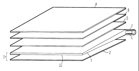
Fig. 4 is a perspective view showing a construction of a
plane illuminating apparatus and a liquid crystal image
display device according to the present invention;
Fig. 5 is a graph comparing a distribution of luminance
of the light conductive plate in the embodiment shown in Fig.
1 to a conventional plate; and
Fig. 6 is a plan view showing a conventional dimming
pattern.
DESCRIPTION OF THE PREFERRED EMBODIMENTS
Embodiments of the present invention will be described in
detail hereinbelow with reference to the drawings.
Fig. 1 schematically illustrates an example of a curve
pattern according to one embodiment of the present invention.
Fig. 1 shows a curve pattern in which a plurality of circles
having a radius R are defined about a number of center points
ri, r2, r3, etc. arranged at fixed constant intervals d on a
straight line X. Such a curve pattern is formed by (concave)
grooves or raised (convex) portions on the surface of a
transparent light conductive plate LG having one edge A near
the line X and the light source 1, and another edge. B which is
farther from the line X and the light source L. That is, on
the light conductive plate LG are formed circular 'J-shaped
_g_
grooves defining curves bl, b2, b3, etc., and circular curves
c1, c2, c3, etc. intersecting the curves bl, b2, b3, etc.
These grooves reflect and diffuse light emitted from the light
source L. As will be apparent from the drawing, tile pattern
density is low at the near edge A while the pattern density is
high near the far edge B. Moreover, each of the circular
curves is substantially perpendicular to the light source L in
the vicinity of the near edge A whereas it is substantially
parallel to the light source L in the vicinity of 'the far edge
B.
Little of the light emitted from the light source L is
reflected and diffused by the V-shaped grooves near the edge A
because of the low groove density and because the curves are
substantially perpendicular to the light source L (parallel to
the Light emitting direction)in the vicinity of the near edge
A. on the other hand, the emitted light is intersects the V-
shaped grooves at a sharp angle near the far edge B where the
curves are substantially parallel to the light source L
(perpendicular to the light emitting direction)in the vicinity
of the far edge B of the light conductive plate LG.
Accordingly, the light reflection increases and the light
dimming effect becomes high. In this manner, the dimming
effect increases as the Light moves from the near edge A
toward the far edge B and, since the light intensity inversely
decreases as the light moves from the near edge A toward the
far edge B, uniform luminosity for the light conductive plate
can thereby be achieved.
~~~.9~.9
_g_
The terms "substantially perpendicular" and
''substantially parallel" herein used mean more or less "close
to perpendicular" and "close to parallel," and not a strict
precision as may be measured by a protractor. The::e terms
should be flexibly interpreted corresponding to various
factors such as uses and object, area, thickness of: the
transparent conductive plate, dimensions of a diffearence in
level of the concave portion and convex portion, and are mere
terms used as one means which represents the change:
progressively from the near edge to the far edge oi: the light
conductive plate. Accordingly, it should be interpreted that
"perpendicular" and "parallel" are sometimes in thsa range of
angles from about 20° to 40°.
The radius R of the circles varies with the size of the
light illuminating apparatus. In the case of a light
conductive plate for a normal liquid crystal panel with a
width between the near and far edges of about 2 to 8 inches
(about 50 mm to 200 mm), the radius is preferably .in the range
of from 50 to 120 mm. The center spacing d between the
circular curves varies depending on the depth of tlhe grooves
or the height (difference in level) of the convex :portion, and
the length of the light conductive distance. Preferably, the
spacing d is in the range of from about 0.3 to 2.0 mm at the
position of the center points (rl, r2, r3, etc.).
Fig. 2 shows a second embodiment of the present invention
using a second order curve in place of a circular curve. In
this embodiment, the apexes of a number of second order curves
are arranged at fixed distance d along a straight line X-X
~4~119._
-10-
adjacent the edge of the plate LG farthest from the: light
source L. Accordingly, the origin points of the second order
curves are also on a straight line. Since the shape of the
secondary curves can be freely changed by varying the
coefficient "a" in the equation:
Y = aXz,
this embodiment is suitable for the design of a pattern in the
case where a circular curve is not successful in providing
uniform luminance.
Fig. 3 shows an embodiment in which the light source is
in an L-shape, and a dimming pattern is designed using
circular curves with center points on the circle Y to produce
a pattern which is widely spaced at the near edge of the light
conductive plate and is dense toward the far edge opposed
thereto.
A pattern which is widely spaced at the near cadge of the
light conductive plate and is dense toward the far edge
opposed thereto may employ, in addition to circles or second
order curves as mentioned in connection with the first and
second embodiments, respectively, third or higher order
curves. In the case where a pattern is formed by a cutting
process, circles or second order curves are suitably employed.
For mass production of light conductive plates having a
present dimming pattern curve, it is preferable to use an
injection molding process.
The pattern of curves, as seen in section, may have any
of suitable concave or convex sectional shapes. Various
shapes such as a V-shape, an angular shape, a semispherical
214'g,~9_
-11-
shape, a polygonal shape and the like can be used. Any
pattern can be produced by injection molding making use of a
mold. A concave V-shape can be made by cutting, wherein the
reflecting angle and the sectional shape are easily
controlled. The depth of a concave portion (a groove) or the
height of a convex portion is preferably about 0.01. to 0.5 mm.
It is possible to continuously change the depth of a
concave portion (a groove) or the height of a convex portion,
when necessary. When the depth is changed, preferably, the
depth is made deeper as the groove is farther from the light
source to improve the dimming efficiency. The inner surface
of a concave portion or the outer surface of a convex portion
can be formed as a coarse surface such as aventurine. The
patterns in the embodiments described above may be formed
making use of translucent or white ink or the like by a
printing method. A vacuum vapor deposition method,, a sand
blast method, and a photoetching method may be also used.
The light conductive plate may have a constant thickness
or may have a wedge-like shape which becomes thinner with
greater distance from the light source, as shown in Fig. 4.
In the case of the plate having a constant thickness, it is
preferable that a light reflecting surface is provided on the
far edge, i.e., that opposed to the edge nearest the light
source side. In the case of the wedge shape, the :reflecting
surface on the far edge is not always necessary, and the
weight of the light conductive plate itself can be reduced.
Materials which may be used for the transparent light
conductive plate include transparent plastics such as acrylic
141~~ 9
-12-
resin, polycarbonate, CR-39, polystyrene. The acrylic resin
is particularly preferable in terms of high transparency and
scratch resistance. The size of the light conductive plate
may be any size, but when it is used as a back light for a
liquid crystal panel, the length of a diagonal line is
normally about 2 to 10 inches.
In a plane illuminating apparatus 3 using the light
conductive plate LG of the present invention shown in Fig. 4,
the light from the light source L is incident on the concave
portion or convex pattern on the back 1 of the light conducive
plate LG, and is thereby reflected. Part of the reflected
light directly moves toward the emitting surface of the light
conductive plate or the other concave portion or convex
portion, but some light passes through the back surface 1 and
is lost. In order to prevent light from passing through the
back 1 of the light conductive plate and be lost, a separate
reflecting sheet 2 is arranged close to the back of the light
conductive plate. An aluminum vapor deposition sheet or a
white light diffusion sheet may be used as the reflecting
sheet.
All of the pattern provided on the light tran:~mitting
plate need not be used as the effective surface of the light
conductive apparatus. For example, at the end of i~he pattern
opposed to the light source, a portion several millimeter to
scores of millimeters from a common tangential line (for
example, line C in Fig. 1) of the pattern can be made to serve
as the effective illuminating end.
~41g19
-13-
The liquid crystal image display device using 'the plane
illuminating apparatus according to the present invention is
basically composed of a liquid crystal display panel 4, a
light diffusion sheet 5, and a plane illuminating device 3. A
prism plate 6 can be provided between the liquid crystal
display panel 4 and the light diffusion sheet 5 to enhance the
luminance at an angle of view only in the specific direction
of view. This prism plate 6 may be arranged in its prism
surface on the side of the diffusion plate or arranged on the
side opposite thereto. A lenticular lens sheet can be used in
place of the prism plate.
Next, a specific example of the present invention will be
described with reference to Figures 1 and 4. A pataern of the
transparent light conductive plate as used in the first
embodiment is composed of a plurality of semicircles. The
radius of the circles is about 90 mm, and the spacing between
the circular curves is about 1.6 mm at the center point. Each
of circles constituting the pattern is composed of a convex
portion (a groove portion), whose section has a V :shape with a
vertex angle of 90° and a height of which is initially about
0.05 to 0.15 mm and becomes continuously deeper as it moves
farther away from the light source.
A fluorescent tube L as a light source is arranged along
the near edge A, and is covered with a semi-circular
reflecting sheet 7 in order to improve the efficiency of
illumination. The light conductive plate LG, which
corresponds to a 4-inch display plate, has a size of about 85
x 70 mm, a thickness of about 4 mm at the end on t:he light
1419r1 ~~
-14-
source side and about 1 mm at the opposite end, and a wedge
shape. The effective illuminating surface terminates about 10
mm inwardly from the common tangential line C of tire pattern
curve.
The luminance of the emitting surface of the light
conductive plate in the apparatus as described above was
examined, the result of which is shown in Fig. 5 and the
Table 1 below. It was found that there is some unevenness in
luminance according to the distance from the light source but
that the luminance is remarkably even as compared with the
conventional devices, achieving a uniform luminance at a high
level of about 3410 nit.
Table 1
Dist. From Light(mm) First Conventional
Embodiment Device
3520 nit 3520 nit
3120 nit 2730 nit
3080 nit 2640 nit
3270 nit 2730 :nit
3540 nit 2820 nit
3710 nit 2960 nit
3730 nit 3160 nit
3750 nit 3220 nit
3650 nit 3210 nit
3380 nit 3300 nit
3160 nit 3330 nit
3010 nit 3520 nit
Average 3410 nit 3095 nit
4 991 9
-15-
The conventional pattern shown in Fig. 6 was formed on
the back of the transparent light conductive plate of the same
size by gradation printing of white ink to prepare a plane
illuminating apparatus, while equally setting other:- optical
conditions. The luminance of the emitting surface of this
illuminating apparatus is as shown in Figure 5 and Table 1.
The average luminance is about 3095 nit, which is lower
by 10% on the average than that of the specific example of the
present invention.
According to the present invention, it is easy to
mechanically adjust many parameters such as the radius of the
circle, curvature of the curve, pitch of the center point,
depth and height of concave and convex portions, sectional
shape and the like. The luminance is high. It is easy to
design a dimming pattern excellent in uniformity. It is
possible to easily produce a light conductive plate as
designed. As a result, it is possible to easily a:nd
inexpensively provide an illuminating apparatus which is not
only high in luminance but also high in uniformity.
Obviously, numerous modifications and variations of
the present invention are possible in light of the above
teachings. It is therefore to be understood that the
invention may be practiced otherwise than as specifically
described herein.