Note: Descriptions are shown in the official language in which they were submitted.
095/01705 ~ 1~ 2 2 8 5 PCT/~94/00171
',
Picture display device comprising a flat-panel type display S
unit.
~ . I
The invention relates to a picture display device
omprising a video drive circuit and a display unit havin~ a
vacuum envelope which is provided with a transparent face plate
with a 1uminescent screen and a rear plate, said display unit
::~ 5 comprising ~a plural1ty:of juxtaposed sources for emitting elec-
. trons, a plurality of electron transport ducts ~cooperating withthe~sources for transporting the electrons in the form of elec-
;~ txon currents:,~ and se1ection means for withdrawing each electroncurrent at predetermined locations from its transport duct and
lO ~for directing said current towards desired pixels of the lumi-
;nescer~t~screen.
:A~p1cture display device of this type is described in
.. `~ t~he non prepublished European Patent Application no. 92204007.6
(PHN 13.96`3)ll:with reference to publication number EP 0550104A2.
The display unit mentioned above is o~ the flat-panel
type, as~ di~sclosed, for example in:European Pate~t Applications
EP~-~A-400~ 750 and EP-A-436 :: ~97. Display units of the flat-panel
.~ type:~are constructi;ons having a ~transparent face plate and,
.~ arranged~at~: a~ smal~l distance :therefrom, a rear plate, which
20~plates are; interconnected: by means of partitions and in which
the~inner:lside:~:of~the~:face pla~e is provided with pixels in the
form~of~ a~ phosphor pattern, one side of which lS provided with
an ~ele~ctrically:~conducting coat1ng ~the combination also being
referred to ~s luminescent screen). If (video information-con-
2:5:,~;~;trol1e~d)i electrons impinge upon the~luminescent screen, a visualimage~is~formed which is visib1e- ~ia the ront si~e of the face
plate. Th~ face plate~ may be ~flat~ or, if de~ired, curved (for
example, spherical or cyl`indrical).
:The display unit described in European Patent Applica-
~30~tions ~EP-A-400¦750 and~ EP-A-436 997 comprises a plurality of
juxtapo ed sour:ces for emitting electrons, local electron trans-
port~ducts cooperating:with the sources and each having walls of
high-ohmic~ ~ electrically substantially insulating material
having a secondary emission coefficient suitable for transpor-
wo g5,0l70~ 2 2 8 5 PCT~B94/00171~
~ 2
ting emitted electrons in the form of electron currents and aselection structure comprising selectively energizable electro-
des (selection electrodes) for withdrawing each electron current
from its transport duct at predetermined extraction locations
facing the luminescent screen, while further means are provided
for directing extracted electrons towards pixels of th~ lumines-
cent screen for producing a pictur2 composed of pixels.
The operation of this known display unit is based on
the recognition that electron transport is possible when elec-
tro~s impinge on an innex wall of an elongate evacua~ed cavitytreferred to as~"compartment~ defined by walls of a high-ohmic,
electrically substantially insulating material (for example,
glass or synthetic material), if an elec~ric field of sufficient
power is generated in the longitudinal direction of the "com-
~ 15 partment" (by applying an ~electric potential difference 'across
;~ the ends of the "compartment").~ The impinging electrons thengenerate~econdary~electrons by wall interaction, which elec-
trons~are attracted to a further~ wall section and in their turn
generate secondary electrons ~again by wall interaction. ~The
O~ circumstances ~(field strength E, ~electrical resistance of the
wa11,;~ secondary~;em1ssion~coefficient ~ of the walls) may be
ahosen to be~such that~ a substantially ~constant ~acuum current
will~flow in the "co~artment~
Start~ing~from the above-ment1oned principle, a flat-
25~panel pi~cture disp1ay~ ùnit can be realised by providing each oneo~a plurality o~juxtaposed~llcompartments n~ which constitute
tr~ansport;ducts~,~wi~th a co1umn~;of;~ext~raction apertures at a side
which~is to~face~a~display~screen.~It will then be pra~tical to
arrange the extraction apertures of adjacent transport du~ts
30; along~para11el lines "extending transversely ~to'~the ~ransport
duc'ts. By~associating selection electrodes arranged 1n rows with
the arrangement of apertures, ~which selection electrodes are
energ~izable~by~ means of a~ first (positive) electric voltage
pu1~se)~ for withdraw1ng electron currents from the "compart-
~ments" via the apertures~o~-a row, or which are energizable by
means~ of a~ ~econd (lower) elec~ric voltage if no electrons are
t
to be locally withdrawn from the "compartments", an addressing
means is provided with which electrons withdrawn from the "com-
`partments" can be directed towards the screen for producing an
~O9S/01705 ` '~ 22:~ PCT~B94/00171
image composed of pixels by activating the pixels.
If non-uniformities occurred from column to column
when controlling the compartments, the- displayed image could
give a stripe-like impression.
It is, inter alia, an object of the invention to
obviate the above-mentioned drawback. In accordance with one
aspect of the invention, the invention provides a picture dis-
play device as defined in claim l.
By modulating the drive signals with the applied video
lO siynal, any luminance can be obtained so that the whole ~pectrum
can be displayed on the display screen. By modulating the drive
signals with the uniformity correction signal, the non-uniformi-
ty can be corrected, and by using pulse-duration modulation of
the drive signals, a simple and accurate output stage can be
15 u~ed.~
An embodiment of the in~entlon as defined in claim 2
enables a uniformity correction by first mul~iplying the applied
video slgnal and the uniformity correction signal to obtain a
signal to c~ontrol the pulse-duration of the drive signals, a
20 simple output stage can be used (~or instance a switch).
An embodime~t of the invention as defined in claim 3
enables~ a uniformity correction by modu~ating for example, the
pulse-duration in dependence on the applied video signal and the
pulse-height in dependence on the uniformity correction signal,
25 ~having the advantage of providing a uniformity correction which
is independent of the pulse-duration.
An embodiment of the invention as defined in claim 4
haa~ the advantage ~;that thè ~switching o~er in the selection
sys~em of the picture display device, occurring between the
~0 pulses of the drive ~aignal and accompanied by a given settling
period, will introduce a (small) error in the high luminance
;portions of the video signal, and will not affect ~he sensitive
dark portions. ~ 1
An embodiment of the invention as defined in claim 5 t
~35~has the advantage that the high frequencies related to one level
pulse-duration modulation axe obviated.
An embodiment of the invention as definedi in claim 6
`~` has the advantage that the switching over in the selection
~;~ system of the picture display device, occurring between the
O95/0l05 ~ 2~ 85 PCT/~94/0017
pulses of the drive signal and accompanied by a given settling
period, will introduce a (small) error in the high luminance
portions of the video signal, and will not affect the sensitive
dark portions.
An advantageous embodiment of the invention is defined
in claim 7. As an example, the first modulation signal is sepa-
rated in a most significant paxt (for instance, the most signi-
ficant bits) and a least significant part (for instance, the
remaining least significant bits) to control the pulse-duration
modulation of two levels.
.~s An embodiment o~ the invention as defined in claim 8
as an example modulates the pulse-duration of a pulse with a
predetermined shape ~(as an example with the shape of a descen-
ding logarithmic function) in dependence on the applied video
signal. The amplitude of the pulse shape, i.e. the pulse-height
is modulated~ in dependence on the uniformity correction signal.
;This embodime~nt offers;the advantage that any desired non-linear
correct~ion (like gamma~ correction) on the drive signals can
easi~ly be implemented. As an added advantage fewer bits may be
. ~ 20 ~required.
An embodiment of the invention as defined in claim 9
has the advantage that the non-uniformlt~y caused by the voltage
; drop acr~ss the~ line~ cathode;~is ob~iated by driving the line
cathode during a period in which no luminance information has to
be displayed. Although this measure can be used advantageously
independently of the pulse-duration modulation of the drive
si~gnals in~dependence upon an applled video signal and a unifox-
mity~correction signal,~ a particular advantage is achieved in
~`' the combination by lowering the amount of uniformity correction
3,0l needed~
These and othe~ a~pects of the in~ention will be
apparent from and elucidate~ with re~erence to the embodiments
described hereinafter.
1`~' ~:~ : `
~` 3s ~ ~ In the drawings
~:: Fig. lA is a diagrammatic perspective elevational
view, partly broken away, of a display unit as can be used in a
display device according to the invention,
Fig. lB is a cross-section throuyh the display unit of
095/0l705 ~1 ~ Z 2 8 5 PCT~394/00l7
1,
~ Fig. lA,
¦ Fig. 2A is a diagrammatic perspective elevational
¦view, partly broken away, of a display unit as can also be used
¦in the display device, which display unit has a preselection and
a ~ine selection,
Fig. 2B is a cross-section through the display uni~ of
Fig. 2A,
Fig. 3 is a block diagram of an embodiment of a dis-
play device accordlng~to the invention,
j 10Figs. 4A: an~ B show embodiments of the drive of an
electron source arrangement.
Fig. 5 shows differen~ modulation methods for modula-
ting the grids with ~ideo information. ~ :
! 15 Figs. lA and lB show a given type of flat-panel dis-
play unit 1 of a picture display device having a display panel
(window) 3 and a rear wall 4~ located oppo~ite said panel. A
:luminescent screen 7 having a repetitive pattern (row~ or dots~
o~, for ;example triplets of red (~), green (G) and blue (B)
20~ luminescing phosphor elements (or monochrome elements) is arran-
ged on the inner surface:of window 3. To be a~le to supply the
required~high voltage, the luminescent sc~reen 7 is either arran-
:
ged on a transparent, electrically conducting layer (for exam-
ple, indium-tin oxide) or is: provided with an electrlcally
25~conduct;ing: layer (for example, AL: backingj. In a preferred
embodiment the :(dot-shaped) phosphor elements of a triplet are
: located at the~vextices of a ~ubstantially isosceles/equilateral
:tr:iangle.~
An electron source arrangement 5, for example a line
30i: cathode which by~means o~ drive elec~rodes provides ai large
: number (for example, 600) of electron emitters or a similar
number of separate emitters, lS ~arranged proximate to a bottom
: plate 2~ which interconnects di~play panel 3 and rear wall 4.
Each of these emitters is to provide a relatively small current
3~5~ so that many t~pes~of cathodes (cold or hot cathodes) are suit-
a~le:as emitters. Each emitter may be arranged separately or, i~
they are combined to one line cathode~ they may be arranged
jointly.~They may have a constant or controllable emission. The
~electron source arrangement 5 is arranged opposite entrance '5
" ~
woss/0170s ~ 2142285 PCT~B94/00l7 ~
',
apextures of a row of electron transport ducts extending sub-
stantially parallel to the screen, which ducts are constituted
by compartments 6, 6', 6'', ..., etc., in this case one compart-
ment for each electron source. These compartments have cavities
ll, 11', 11'', ... defined by the rear wall 4 and partitions 12,
~r~; 121 ~ 12~ At least one wall (preferably the rear wall) of
~; each compartment is made of a material which has a suitable high
electrical resistance in the longitudinal direction of the
compartments for reali~ing electron transport (for example,
ceramic material, glass, synthetic material - coa~ed or uncoated
-) and which have a secondary-emission coefficient ~ ~ 1 over a
gi~en range of prlmary electron energies. It is alternatively
pQssible to construct (for example,-the rear wall) from "isles"
insulated from each other (in the longitudinal direction of the
compartments~ so as to obtain the desired high electrical resis-
tance in the transport direction.
The ~electrical~resistance of the wall material has
such a~ value in the transport direction that a minimum possible
~ total amount of current (preferably less than, for example 10
`~ 2~0 ~mA) will flow in the walls in the case of a field strength in
thè~ axial direction in the compartments of the order of one
hundred to several hundred Volts per cm~required for the elec-
tron transport. A voltage Vt which generates the field strength
required for the transport is present in operation between an
~25~ upper rim 200 and a lower rim 201 of the rear wall 4. By apply-
ing a voltag~ of the order of sevexal dozen to several hundred
Vvlts (value~ of the voltage is dependent on circumstances)
between the row 5~ of the electron sources and grids G1, G2
arranged at inputs of the compartments 6, 6', 6'', ..., elec-
30l t~ons~ i.axe~ ,accelerat!ed~ from~ the electron sources towards thecompartments, whereafter~ they impin~e upon the walls in the
compartments and generate secondary electrons. The electrons can
be withdrawn, for example, row by row from .he compartments via i;
apertures 8, 8', ... in a selection plate 10 energized by means
of electrodes 9, 9', ..., (see Fig. lA), and accelerated towards
the luminescent screen 7 by means of an acceleration voltage
~; applied in operation between the selection plate and the lu~i-
nescent screen. Horizontal partitions 112, 112', 112 ", ... are
arranged between the display panel 3 and the selection plate lO.
~ ~ 095/01705 '` ~ 21 ~ ~ ~$ ~ PCT~B94/00171
~1
Instead of the partitions shown, it is alternatively possible to
use apertured plates.
In this case the invention utiiizes the aspect disclo-
I sed in European Patent Applications EP-A-400 750 and EP-A-436 997 that vacuum electron transport within compartments having
~i walls of electrically insulating material is possible if an
electric field (Ey) of su~ficient power is applied in the,longi-
tudinal direction of the compartment. The contents of European
Patent Applications EP-A-400 750 and EP-A-436 997 or United
States Patents corresponding thereto are herein incorporated by
reference.
Figs. lA and lB show the principle of a display unit
I o~erating with single selection ~as described hereinbefore).
Figs. 2A and 2B show the principle of stepped selecti-
on. Stepped selectlon i5 herein understood to mean that theselection from the compar~ments 6, 6~, 6~, ... to the lumin~s-
1~ cent screen 7 is realised in at least two steps: a first (coar-
se) step for selecting, for example, the pixels and a second
-~ (fine) step for selectlng, for example the colour pixels. The
~;~20 space between the compartments and the luminescent screen 7,
which is arranged on the inner wall of display panel 3, accom~o-
dates an active colour selection system lOO which comprises an
(active) preselection plate' lOa, a spacer plate lOb and an
(active) (fine-)selection plate loc. Structure lOo is separated
from the luminescent screen 7 by a flu-spacer structure lOl, for
example an apertured electrically insulating plate.
Fig. 2~B shows in a diagrammatical cross-sec~ion a part
of the display device of Fig. 2A in greater detail, particularly
the acti~e colour selection plate structure lOO which comprises
~30, a preselection plate iOa with~extraction apertures 8, 8', 8'i,
... and a fine-selection plate lOc with groups of.apertures R,
G, B. The apertures~R, G, B are generally positioned in a trian-
gle, but for~ the sake of clarity all three of them have been
shown in ~he cross-section in Fig. 2s. Each extraction aperture
~35 8, 8'~ etc.~is associated with three fine-~election apertures R,
~;~ G1 3 in this case. Other numbers are alternatively possible, for
example 6 fine-selection apertures for each preselection apertu-
re, etc. An intermediate spacer structure lOb iB arranged be-
twe~n the preselectlon plate lOa and the fine-selection plate
,~ .
~ 214228S
,~ WO 95/0170~ PCT/IB94/0017
. ~ A 8
10c. This structure accommodates communication ducts 30, 30',
30'', ... having a cross-section which is chosen to suit the
shape of the phosphor colour pixels (for example, circular or
triangular triplets).
The electron transport ducts 6, 6', 6'', .......... are
¦ ~ormed between the structure 100 and the rear wall 4. To be able
to extract the electrons from the transport ducts 6, 6', 6'',
... via the apertures 8, 8', 8'', ..., pierced metal preselecti-
on electrodes 9, 9', 9'', ... are arranged on the screen-sided
surface of the plate 10a.
The walls of the apertures 8, 8', ... are preferably
metallized completely or partly, but there is preferably no or
little electrode metal on the surface of plate 10a on the side
where the electrons land. This is done to ensure that no elec-
trons remain on a selection electrode during addressing (i.e.
~; ~ the eIectrode must draw a minimum current).
Another solution to the problem of drawing current isto ensure that there is electrode metal on the selec~ion surface
where the electrons land, but this metal should be given such a
lar~e secondary emission coefficient that the preselection
electrodes do not draw any net current.
Similarly as the plate 10a, the screen-sided surface
`~ of the apertured fine-selection plate 10c is provided with
(fine-)selection eIectrodes 13, 13', ... for realising, for
;~ 25 example colour selection.~Here again the apertures are prefera-
bly metallized completely or partly. The possibility of electri-
cally interconnecting fine-selection electrodes is important in
this respect. In fact, a preselection for each pixel has already
taken place and, in principle, electrons cannot land at the
3~i wrong location (on the wrong pixel in this example). This~means
that, in principle, only one group or a small number of groups
of three separate ~ine-selection electrodes is required for this
form of fine selection. For example, the drive is ef~ected as
follows, but there are also other possibilities. The pres~lecti-
;~35 on electrodes are brought t~ a potential substantially linearlyincreasing with the distance to the electron source arrangement
5, for example, by means of a suitable resistance ladder.
One or more picture lines are selected ~y applying a
positive voltage pulse of, for example, 200 V to the desired
;3 ;
;~,t ~r) 351~171~5 ~ 1 9 ~
8 5 PCTnB94/~0171
preselection electrodes used for selecting these picture lines.
~ Colour pixels are addressed by applying shorter pulses having an
3 amplitude of, for example 300 V to the fine-selection electro- !
des. The ~ine-selection electrodes preferably have such an
5 electrical resistance, or are connected to external resistors in t
such a way that they safeguard the electronic circuits (control-
ling the drive) against breakdown from the luminescent screen.
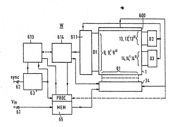
3.~ Fig. 3 shows a display device W in which the invention
3 can be used. The display device receives an input video signal
1~ 10 Vin at an input 61. The input video signal Vin is applied to a
video signal processing circuit 65. The display device receives
a synchronizing signal sync at an input 62. The input 62 is
co21nected to a syncnronization processing circuit 63. This
synchronization processing circuit supplies synchronizing sig-
:~ 15 nals to a clock generator 613 and ~efines the televi~ion stand-
ard of the incoming video signal. The incoming video signal may
~:comprise, for example Y, U, V signals (or R, G, B signals). If
the incoming video signal comprises Y, U, V signals, a conversi-
;~ on to R, G, B ~si~nals will have ~to take place in the video
signal processing circuit:65 so that ultimately the different
phosphors (red, green and blue) can be driven on the display
panel 3. This conversion of Y, U, V signals to R, G, B signals
may be effected by means of a ma~rix circui~. It is possible to
carry out this conversion before the video signal is written
25~ nto the memory MEM, or during the processing operation in the
~ideo signal processing circuit 65, or after the ~ideo siynal
proces~in~ circuit ~5. The video: signal is stored, for example,
line-~equentially in the video ~ignal processing circuit 65
under the control of a write clock which is generated, for
30l example~,! by the clock generator 613. The video signal is sup-
plied line by line (for example, for each colour line (R, G, B)
in the case of a colour display screen) at an output of the
video signal: proces~ing circuit under the control of a read
clock generate~ by a clock generator 614 and is applied to the
~; 35 video drive circuit 34. In this ~ideo drive circuit the video
information of, for example a (colour) line is written under the
control of the clock generator 614 and subsequently applied in
parallel to the Gl (or G2) electrodes which are arran~ed at the
inputs of the compartments 6, 6', 6'', ... (see Fig. 1) of the
.~ .
WO95/01705 ~ 2~S PCT/~94/0017
display unit 1, after which the video information is displayed
on the display panel 3. The lines and pixels are selected by
means of a selection driver 611. The driver is controlled by a
clock signal from clock generator 614. After each clock pulse
l 5 the drive circuit D1 applies new drive voltages to the selection
! electrodes 9, 9', 9'' ...... under the control of the selection
driver 611 (see also Fig. lA). The selection driver receives the
information about the drive voltages, for example, from a look-
up table or from an EPROM. The display unit 1 has a structure as
described hereinbefore (see Fig. lA~.
The synchronization processing circuit 63 defines the
line frequency, the field frequency and if the display device is
suitable for displaying video signals of different TV standards
and/or different aspect ratios, for example also the TV standard
and the aspect ratio with reference to the incoming video sig-
nal.
The video signal processing circuit 65 stores the
incoming video signal, for example, line-sequentially in a
memory MEM, being part of the video signal processing circuit,
under the control of a control section PROC. The control section
receives information (i~ necessary) about the relevant TV stand-
ard and the aspect ratio from the synchronization processing
circuit. The control section further receives the write clock
and the read clock for writing and reading the video signal,
respectively, from the clock generators 613 and 614. The control
section may also ensure conversion to the double field frequen-
cy.
If the number of incoming video lines stored in thememory does not correspond to the number of display lines asso-
30i ciated` with the display~unit, the video signal processing cir-
cuit is to ensure a line and pixel distribution associated with
the display unit. Th~ incoming video signal havin~ n lines
(dependent on th~ standard) must be converted by the video
signal processing circuit into a video signal having m lines
(the number of lines of the display panel 3). There are two
; possibilities, namely either n > m or n ~ m (at n = m the video
signal does not need to be converted).
The video signal may be written into the memory MEM ln
the form of R, G and B signals. After processing under the
O95/01705 21~ 5 PCT~B94100171
control of the control section PROC, the video signal is read
out, for example, in the form of R, G, B signals again.
Figs. 4A and 4B show examples of driving the line
jcathode k(5) and thereby keeping it at the desired temperature.
5 Since the line cathode has a resistance, there will be a voltage
drop across the line cathode if a voltage or a current is pre-
sented to it. The resistance of the line cathode is necessary to
heat the line cathode, but this will cause a difference in the
t~number of electrons emitted by the line cathode in the different
lO ducts. To prevent this, ~the choice may be made to present a
voltage across or a current into the line cathode during the
line retrace periods only. In Fig. 4A this is realised by apply-
~ing the lin retrace pulses which are used for generating the
Jhigh voltage to the line cathode k via a ~ransformer Tr and a
~15 diode D. The diode ensures that the voltage is present across
the line cathode during the retrace pul~e only. Fig. 4B shows an
example in which the same effect is achieved by presenting a
valtage~to the line cathode during~ the line retrace periods
~ only, starting from a DC source V which is connected to the line
`~20 cathode ~ia a switch S.~ The switch S is controlled by a pulse
generator P (for example, coupled to the line retrace pulse). In
an alternative solution the line cathode may be driven continu-
ously and the voltage drop can be corrected by means of the Gl
electrode drive.
~25 ~ n an embodiment of a display device according to the
`~ invention use is ~made of~ a thermal filament in an inverted
triode configuration: the drive~electrode~ are "behind1' the
;~ f;ilament. The required drive ~oltage iB of the order of lO Vtt,
the capacitance is ~determined by the supply filaments or tracks
30~ or chip on gla~ss ~of!the or~ r of lO pF) and~the leakage cur-
rents are~very low.
In the drive o~ this display device there are a number
of~e~sential differénces~from a cathode ray tube ~CRT) drive. In
a CRT the three colours are parallel emitted and the pixels (on
35~ o~e line) are sequentially emitted. This- invol~es three sub-
systems which must operate at very high frequencies and at which
mutual differences lead to an error in the colour balance. In an
embodiment of a display device according to the invention a
large number of columns is driven in parallel and the colours
WOg5/0l705 ~ PCT/~9410017
are driven sequentially. The parallelism implies that the emis-
sion frequencies are relatively low, and since each gun drives
~, all three colours, emission errors do not lead to errors in the
'~ colour balance. The mutual equality of the sourc~s is, however,
essential because this corresponds to a column-to-column unifor-
mity to which the eye is very sensitive. Another result of this
system is that differences between the colours correspond to a
larger dynamic range of the emission. In a number of cases this
could easily be compensated iIl a modulation system as described
hereinafter with reference to Fig. 5, but it is probably simpler
to start from the least efficient colour and to adapt the two
~ other phosphors thereto. Extreme differences are not foreseen at
'~ t-he moment. There are some important causes for column-to-column
non-uniformity.
15As described above a voltage drop across the filament
xesults in a uniformity error. This can be corrected by means of
a feed forward control or prevented by pulsatory heating of the
filament in the non-emissive period. Moreover, a variation of
~; emissive properti~s of the filament surface (temperature, elec-
tron emission potential and contamination) leads to errors.
Under normal vacuum circumstances the emission will be complete-
ly space charge-limited, hence independent of the filament
surface.
A variation of the filament geometry initially does
; 25 not have any influence on the uniformity, but the distance
i~between the filament and the electrodes does. Finally, a varia-
tion of the efficiency o~ the filament influences the uniformi-
ty.
In addition to this column-to-column ~non-~uniformity,
30 the li~e-to-line uniformity should also be ensured/corrected.
Particularly for a filament at half the height o~ the display,
the lines in the middle will have to be corrected.
Xn order to correct the above-mentioned uniformity b
errors, the video si~nal can be corrected with a correction
35 factor in a multiplier circuit without having to extend the
normal dynamic range of the video signal. It does not matter
whether the correction is realised in pulse height or pulse
width. In principle, a distinction can be made between:
l. no correction,
~.
.., ' 1~
~ O~5/01705 ~2 2 8 5 PCT~Bg4/00171
13 - . .
2. correction in accordance with a fixed setting realised by the
manufacturer,
3. correction in accordance with a control realised by the
manufacturer,
4. correction irl an intermittent feedback, for example when the
displa~ device is switched on, or during the field retrace
period,
5. correction in a direct feedback per column.
A memory element, for example the capacitor of an
analog gated integrator, or a digit:al memory is essential for
items 2, 3 and 4. For item:4, it is sufficient to use a single
detector for all columns combined:: during the measuriny cycle
only cne:column is switched on and detected and fed back at a
common measuring electrode. For item 5 a measuring electrode per
column is required, which doubles the number of contacts and
neces:sitates a separate det~ection circuit per:column. With such
detector means, a test signal applied preferably during the
field retrace time to the video dri~e circuit 34 and transported
by:the transport: ducts 6, 6', 6'', ... can be measured for
~: 20 obtaining an eficient uniformity control. Advantageous use is
:~ made of the detector 600 (see~Fig. 3) as further described in
European Patent Applications EP-A 0 400 750 and 92204007.6 (PHN
13.963)~, ~or corresponding US Patents whose contents are herein
incorporated~by~reference. During the field retrace time, a test
~2~5 s:ignal is applied to the:~ideo input of the video drive circuit
34,:~for example during~a number of line trace periods. Tn this
: embodiment the detector is~a~ranged~above the display unit 1 and
: comprises a measuring element per:compartment 6, 6', 6'', ...
which measures the number of electrons arriving at the top of -.
3 the relevant compartment. The detector compares the measurements
of all measuring elements~for example, with a re~erence signal)
and supplies: a signal so as to compensate this difference. The
detector :thus detects a possible difference between the diffe-
rent channels, which difference can be either corrected in the
35~video drive~circuit 34 itself or fed bac~ to ~he video signal
processing circuit 65, PROC in which the required correction is
:: then performed together with the different operations. ~3
Dependent on the errors ~.ade and/or with reference to
the desired resolution/accuracy it is possible to make a choice ~.t
:
WogS/01705 ~ Z8S 14 PCT/~94/00171 ~
between the different uniformity correction methods mentioned
~:i under items l to 5.
To display the incoming video signal on the display
screen, the number of electrons which is sent into the ducts by
the grid Gl ~G2) must be modulated. This can be done in accor-
dance with a number of different methods as shown in Figs. 5A to
SE.
Fig. 5 shows the signals for 6 differen~ intensities
~9/16, l/16, 2/16, 4/16, 8/l6 and 16/16).
Fig. 5A shows voltayes which occur in an embodiment of
a video drive circuit 34 when usin~ pulse height modulation. The
required pulse repetition frequency is reasonably low (~ l
MH~). The pulse height can be fixed both in an analog and a
digital manne~, but in both cases i~ is not trivial to ensure
the required mutual equality between the columrls. In the analog
system crosstalk and variations in offset and gain are a pro-
~ blem, and the digital system ~equires a DAC per column. When
9 : using ~ulse helght modulationj a column-to-column uniformity of
the guns is required throughout the dynamic range.
~1 20 Fig. 5B shows voltages which ocGur in an embodiment of
a video drive circuit 34 when using pulse width modulation. This
signal results in a gamma of l.00. The~ output stage is very
simple and accuxate ~for example, a switch) and can al50 be
fairly easily extended by means o~ a uniformity correction: it
. ~ i
J;~25 is necessary to correct only one level (i.e. the gain) and the
system is further linear by nature. The gain can be performed as
a multiplication factor on the linear video signal or as a
correction of the amplitude. In the latter case the correction
is by nature correct throughout the range: the amplitude is
30 adapted until the effective emis~ion of all sources i5 the~ same
and the video signal is "independent"-modulated thereon in pulse
width and i~ thus linear.
~; The pulse width can be simply generated in an analog
or a digital form. A drawback of the gamma = l.00 is that, since
our perception has a logarithmic character, ~ery small grey
scales are neces~ary in the dark portion. Analog processing then
already soon involves extra noise in dark portions, while also
crosstalk may occur due to all switching neighbouring signals.
Digitally generated signals result in a very great accuracy, but
::
~ O95/01705 lS 2 1 ~ 2 8 5 PCT/~94/00171
then very high frequencies are used: lO0 Hz HDTV with colour and
column multiplexing involves a pulse period of approximately 2.5
microseconds, i.e. lOO MHz resolution for a small number of grey
scales of ~56. As is shown in Fig. ~B, the leading edge of the
pulse is modulated instead of the customary trailing edge. This
~! has the advantage that, since the selection syste~ switches over
between the pulses and is accompanied by a given settling peri-
od, a (relatively) small error is obtained for a signal having a
large intensity as a result of a selection which is still insuf-
ficiently stabilized, while the other intensities are not noti-
ceably influenced.~ However, if the trailing edge is modulated,
the dark portions are relatively strongly influenced by a selec-
tion which is not yet stabilized. For all switched display
screens, leading edge modulation thus yields ampler time margins
than trailing edge modulation.
Fig. 5C shows ~oltages which occur in an embodiment of
a video drive circuit 34 when using a first mixed form of pulse
height and pulse width modulation. Here, the separate bits of
~ ;the intensity signal are separately~ emit~ed with respect to
;~20 time. Now, a plurality~of individual pulses may be consecutively
~ produced, as is shown for the first period of relative intensity
`~ 9/16. In this embodiment the output stag~e reduces to a single
switch per column and~the height of the consecutive bit levels
; ~can be controlled centrally. The frequencies are not too high. A
problem of this embodiment is that separate bit levels should
correspond accurately to the associated emission levels, i.e.
they should not correspond to the voltage levels. In fact, the
signals are added together ~a~ emission wi~h respect to time.
This means that all bit levels must be adjusted to the gamma
0~1 characte~istic oflthe~ guns and that non-uniformity of the guns
cannot be corrected without losing the advantage of the central
it level control. The pulse-height of the separate pulses may
aIso be chosen in an ascending order.
Fig. 5D shows voltages which occur in an embodiment of
~35 a video drive circuit 34 when using a modulation in which the
; pulse width signal is modulated with a descending pulse height.
The result is that the effective gamma of the pulse width signal
will be much larger than l ~here, for example 2 when it is
~; assumed ~hat the cathode reacts linearly proportionally). Conse-
WOg5/01705 2 1 4 2 ~ 8 5 16 PCT~B94/0017 ~
quently, smaller grey scales in the dark portions are automati-
cally obtained, which for an analog circuit yields less noise
and for a digital circuit yields fewer required bits and hence a
lower frequency. A drawback i5 that a possible lack of uniformi-
ty throughout the pulse height characteristic results in errors.
Otherwise, the drivers themselves may have a very good uniformi-
ty because the pulse height sweep can be generated centrally so
that the output stages have the character of a switch again. Any
desired gamma or other non-lin~arity correction can be set in a
very simple manner by means of the centrally generated pulse
height sweep. Non-uniformity of the guns directly leads to large
errors. The pulse height sweep waveform can be chosen to fit
with the desired non-linearity correction, and need not be a
straight line. In case of an ascending waveform the pulse-dura-
tion modulation ca be performed on the trailing edge.
Fig. 5E shows voltages which occur in an embodiment ofa video drive circuit 34 when using another mixed form of pulse
height and pulse width modulation. Here, the drawback of the
high digital frequencies of the pure pulse width moduiation of
Fig. 5B is obviated by dividing the signal into two parts.
First, the most significant part of the signal is emitted in
pulse width. Then, the least significant bits are emitted in
pulse width at a much lower pulse height. This leads to a lea-
ding edge modulation having a large~pulse height for coarse
~5 control and a trailing edge modulation ha~ing a low pulse height
~or the fine control. An example thereof is a total of 9 bits
accuracy, di~ided into 6 MSB and 3 LSB. A total pulse duration
of a maximum number of 64 ~ime steps is then obtained in the
coarse part, plus 8 time steps in the fine part at an emission
~3~0l le~el;of 1/8 of the coarse part. This yields a total of 72 time
steps, i.e. acceptable frequencies, and still a 9-bit resoluti-
on. The outpu~ stage still has the level of a single switch. It
is a problem again to control the ~SB pulse height a~ (for
example) 118 of ~he emission level of the MSB pulse height, but
as far as accuracy and complexity are concerned this is much
~less diemanding as the modification described hereinbefore with
reference to Fig. 5C. In other words, small differences between
the guns themselves can probably be compensated for. It is also
possible to first emit the low pulse height in pulse-width and
, ` ~ 095101705 - 214 2 2 8 5 PCT~B94/00l71
~ l7
then the high pulse height in pulse width.
A choice can be made from the following preferred
methods.
~ No uniformity correction necessary: embodiments shown in
Fig. 5D or possibly 5E. Fig. 5D shows a freely adjustable
gamma correction, which may have its advantages for the
previous video processing operation (number of bits). Fig.
SE provides additional possibilities for a high grey scale
xesolution at acceptable frequencies, but is slightly more
critical in matching the MSB and LSB emission levels. In
Fig. 5D this is not very critical to the eye, because there
are no discontinuities in~the transmission.
-- Only gain correction necessary: this is always possible and
I simple, particularly in the linear systems, see Fig. 5B or
j 15 5E. In principle, it is possible to choose pulse width
correction (video signal) or pulse height correction.
Large differences in gun characteristics: see Fig. 5B or
`~ 5E. In Fig. 5B it is possible to choose between pulse widthcorrection (video signal~ or pulse height correction of
ea~h column. In Fig. 5E both emission levels should be :
controlled per coIumn.
Generally, vid:eo signals are transmitted and processed
colour-parall~l and pixel-sequentially. This means that a se-
ies-parallel conversion has to be performed somewhPre in the
` 25 ~system. The obvious choices are analog versus digital and shift
reyister versus bus distxibution. Bus distribution requires
fewer components but imposes strict requirements on the fan-out
of the bus drivexs. ~Shift registers in analog form may yield a
cumu1ative error. An analog form may be a CCD register (charge
30l transport) ! or a sample!-and-hold register (voltage transport). ~
:
A related point is the information current density, -~
when, for example l00 Hz HDTV is~applied. In the traditional
~: :
serial structure, very high frequencies are associated there-
with. A possibility of decreasing the frequency is the use of
.
3S two or more parallel processors, for example one for the left- -~
hand par~ and one for the right-hand part, while the number of
processors is reduced in display screens on which less stringent
requirements are imposed, so that this will have a cost-decrea-
sing effect.